patent · US5488234
Semiconductor element having bivalent and VI group element and an insulating layer
30 January 1996
Page 1 — bibliographic record
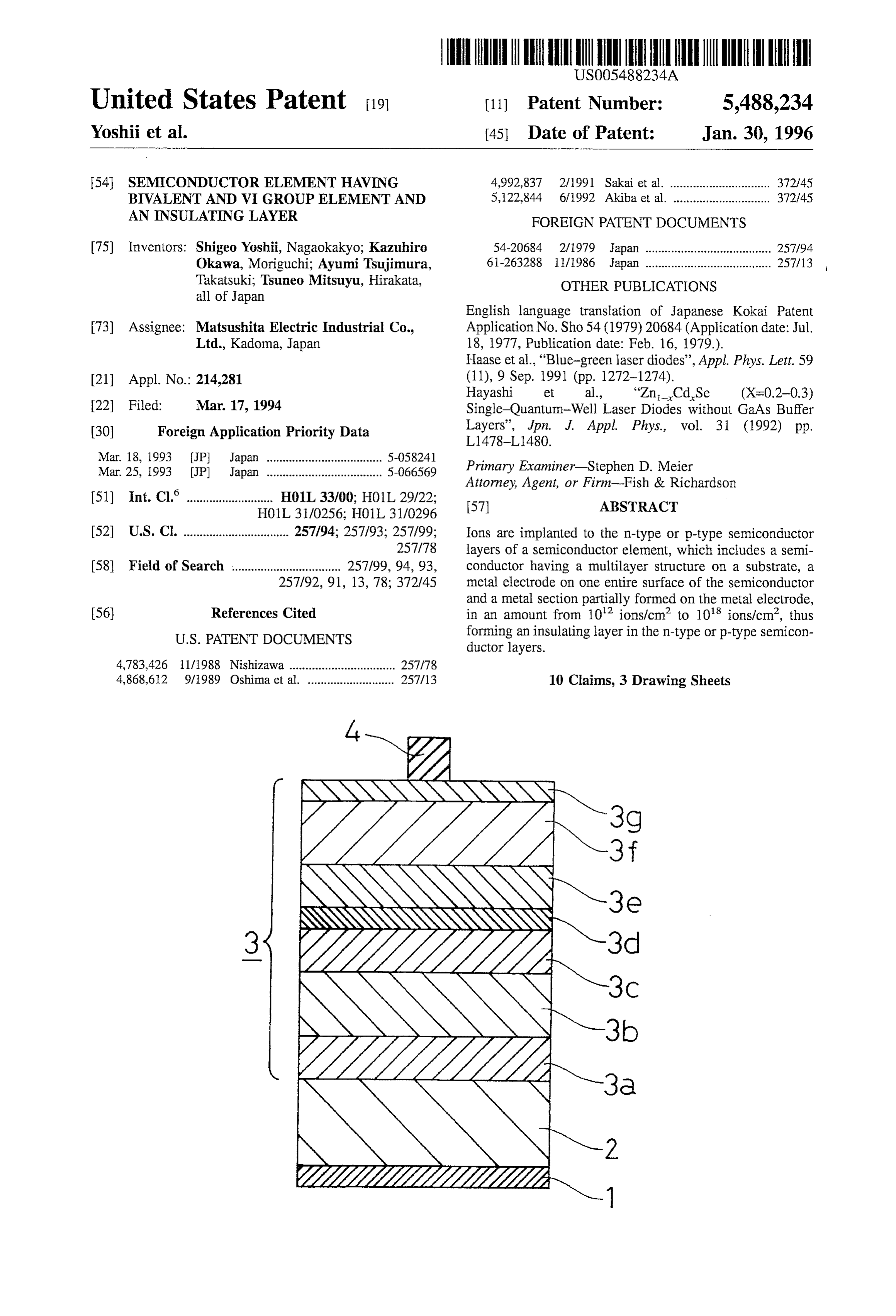
United States Patent 19 11 Patent Number: 5,488,234 Yoshii et al. (45) Date of Patent: Jan. 30, 1996 54 SEMICONDUCTOR ELEMENT HAVING 4,992,837 2/1991 Sakai et al. ............................... 372/45 BVALENT AND VI GROUPELEMENT AND 5,122,844 6/1992 Akiba et al. .............................. 372/45 AN INSULATING LAYER FOREIGN PATENT DOCUMENTS 75) Inventors: Shigeo Yoshii, Nagaokakyo; Kazuhiro 54-20684 2/1979 Japan ....................................... 257/94. Okawa, Moriguchi, AyumiTsujimura, 61-263288 11/1986 Japan ....................................... 257/13 Takatsuki; Tsuneo Mitsuyu, Hirakata, OTHER PUBLICATIONS all of Japan
English language translation of Japanese Kokai Patent 73) Assignee: Matsushita Electric Industrial Co., Application No. Sho 54 (1979) 20684 (Application date:Jul. Ltd., Kadoma, Japan 18, 1977, Publication date: Feb. 16, 1979.). Haase et al., "Blue-green laser diodes', Appl. Phys. Lett. 59 21 Appl. No. 214,281 (11), 9 Sep. 1991 (pp. 1272-1274). Hayashi et al., "Zn-CdSe (X=0.2-0.3) 22 Filed: Mar. 17, 1994 Single-Quantum-Well Laser Diodes without GaAs Buffer 30 Foreign Application Priority Data Layers', Jpn. J. Appl. Phys., vol. 31 (1992) pp.
Mar. 18, 1993 JP Japan .................................... 5-058241 Primary Examiner–Stephen D. Meier Mar. 25, 1993 (JP Japan .................................... 5-066569
Attorney, Agent, or Firm-Fish & Richardson 51) Int. Cl. ........................... H01L 33/00; H01L 29/22; 57 ABSTRACT
52 U.S. Cl. ................................. 257/94; 257/93; 257/99; Ions are implanted to the n-type or p-type semiconductor 257/78 layers of a semiconductor element, which includes a semi 58 Field of Search .................................. 257/99, 94, 93, conductor having a multilayer structure on a substrate, a 257/92, 91, 13, 78; 372/45 metal electrode on one entire surface of the semiconductor and a metal section partially formed on the metal electrode, 56) References Cited in an amount from 10' ions/cm to 10' ions/cm, thus
ductor layers.
4,783,426 11/1988 Nishizawa ................................. 257/78 4,868,612 9/1989 Oshima et al. ........................... 257/13 10 Claims, 3 Drawing Sheets
NYN
Page 2
Drawing sheet — no readable text.
Page 3
Drawing sheet — no readable text.
Page 4
Drawing sheet — no readable text.
Page 5
SEMCONDUCTOR ELEMENT HAVING selected from the group consisting of S, Se andTe is used for BIVALENT AND VI GROUPELEMENT AND the semiconductor.
AN INSULATING LAYER It is preferable that the semiconductor element is a semiconductor laser element.
It is preferable that the insulating layer is a current
FIELD OF THE INVENTION blocking layer.
The invention relates to a semiconductor element, a
It is preferable that the semiconductor laser element comprises a semiconductor having a multilayer structure on semiconductor laser element, and methods of manufacturing a substrate, a metal electrode on one entire surface of the the same. More particularly, the invention relates to an 10 semiconductor and a metal Section formed partially on the insulator for a semiconductor element. metal electrode, and that the semiconductor excepting the area immediately below the metal section is insulated by the
BACKGROUND OF THE INVENTION implantation of ions, thus forming the current blocking layer.
In order to prolong the life of a semiconductor laser 15 It is preferable that the metal section, formed partially on element, it is necessary for an insulating layer to release the metal electrode, comprises laminated metal layers which efficiently to the outside heat generated by the semiconduc form stripes on the metal electrode.
It is preferable that the thickness of the metal electrode is
SiO2, polyimide resins or the like have been convention from 10 nm to 1 um.
ally used for insulating layers of semiconductor laser ele 20 It is preferable that the thickness of the metal section is ments. (See Hiroyuki Matsunami, Semiconductor Technol from 0.1 un to 10 um.
ogy, Shoukoudo, pp. 214, or Applied Physics Letters, vol. It is preferable that the semiconductor is an n-type semi 59, pp. 1,272 (1991).) However, SiO, and polyimide resins conductor, and that the implanted ions are I group or V group have no sufficient thermal contacts with semiconductors, element ions.
and their thermal conductivities are too weak to radiate heat 25 efficiently. Therefore, conventional semiconductor laser ele It is preferable that the semiconductor is a p-type semi ments having SiO, or polyimide resins as insulating layers conductor, and that the implanted ions are III group or VII have poor endurance. group element ions.
It was also impossible to apply n-type semiconductors 30 at The least semiconductor element of the invention comprising one bivalent element and at least one VI group anywhere above the active layers of conventional semicon element is manufactured by implanting ions in an amount ductor laser elements. In conventional semiconductor laser elements, the active layers and the insulating layers are apart from 10° to 10' ions/cm in the n-type or p-type semi from each other. If an n-type semiconductor with high conductor layers at 10 to 10 Tort vacuum, thus forming an insulating carrier mobility is applied between the active layer and the 35 layers. layer in the n-type or p-type semiconductor insulating layer, current is diffused in a horizontal direction and cannot be confined to the active layer. Therefore, in It is preferable in this method that the incident angle of
conventional Semiconductor laser elements, n-type semicon ductors are applied anywhere below the active layers while It is preferable in this method that the substrate tempera p-type semiconductors with a low carrier mobility are 40 ture during the implantation of ions is 0°-300° C. applied anywhere above the active layers. However, because It is preferable in this method that the ion beam current of high top electrode resistance and the Schottky barrier density during the implantation of ions is 10 nA/cm-l between the top electrodes and the p-type semiconductors, HA/cm.
the operating voltage of conventional semiconductor laser It is preferable in this method that the semiconductor elements tends to become high, and heat is generated at the 45 element is a semiconductor laser element, and that ions are top electrodes of the elements. implanted via a metal section and a metal electrode of the semiconductor element.
SUMMARY OF THE INVENTION It is preferable in this method that the metal section, formed
In order to solve the problems of conventional semicon 50 metal layers partially on the metal electrode, comprises laminated ductor laser elements, this invention provides a semicon which form stripes on the metal electrode. ductor element which has an insulating layer having good It is preferable in this method that the thickness of the thermal contacts with semiconductor materials, high thermal metal electrode is from 10 nm to 1 um. conductivities and sufficient insulating properties. The It is preferable in this method that the thickness of the invention also provides methods of manufacturing the semi 55 metal section is 0.1-10 um.
conductor element of the invention. It is preferable in this method that the semiconductor is an In order to accomplish the above and other objects and n-type semiconductor, and that the implanted ions are I advantages, the invention provides a semiconductor element group or V group element ions. comprising a compound of at least one bivalent element and It is preferable in this method that the semiconductor is a at least one VI group element, and an insulating layer which 60 p-type semiconductor, and that the implanted ions are III is formed by implanting ions in an amount from 10' to 10' group or VII group element ions. ions/cm’ into n-type or p-type semiconductor layers. It is preferable in this method that the acceleration voltage It is preferable that the thickness of the insulating layer is of ions is from 10 keV to 1000 keV. from 10 nm to 10 um. It is preferable in this method that the implanted ions are It is preferable that a compound of (1) at least one bivalent 65 nitrogen ions, that the acceleration voltage of ions is from 10 element selected from the group consisting of Zn, Cd, Mg, keV to 1000 keV, and that the semiconductor where the ions Mn, Hg and Ca and (2) at least one VI group element are implanted is an n-type semiconductor.
Page 6
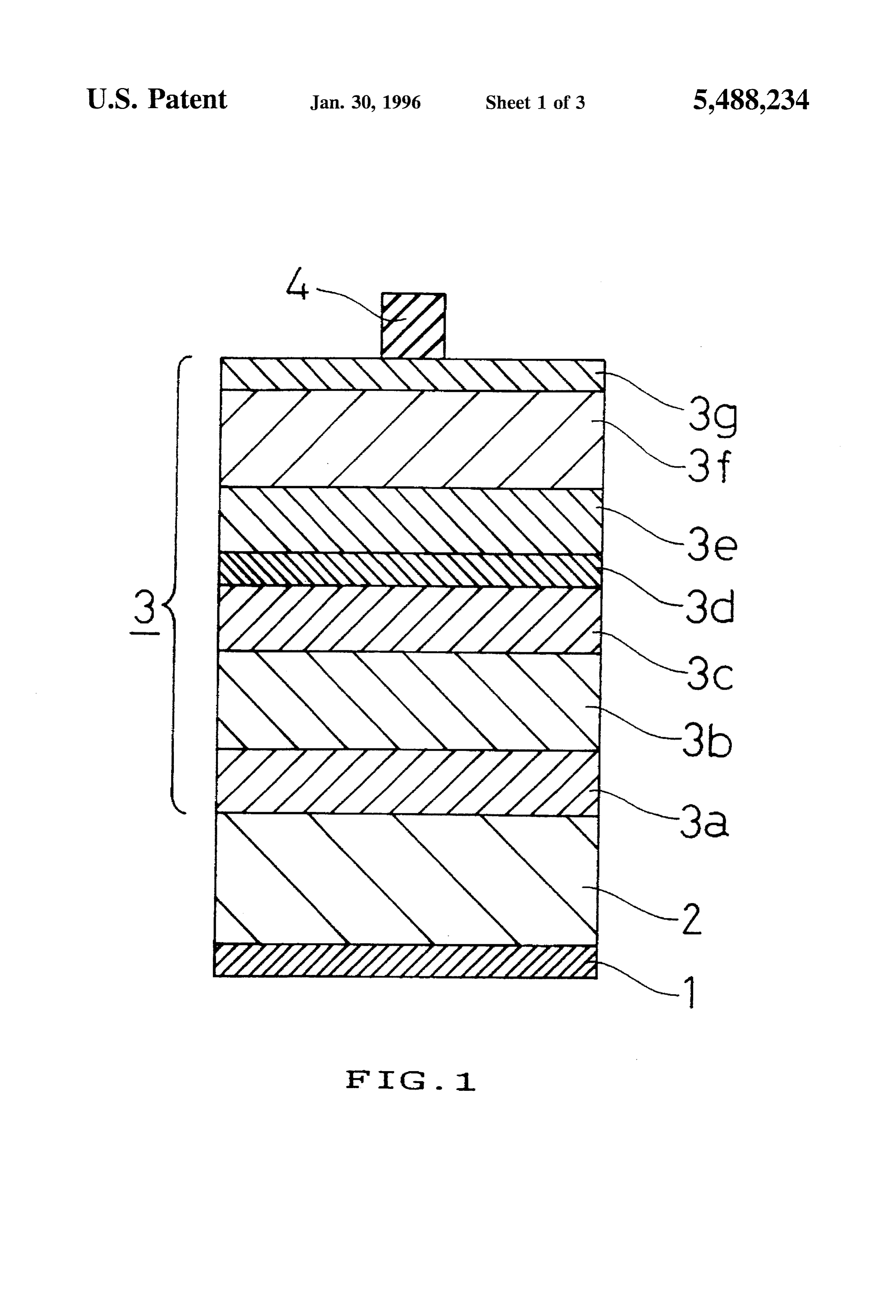
BRIEF DESCRIPTION OF THE DRAWINGS layer of the invention also has higher radiation properties FIG. 1 shows a cross-sectional view of a semiconductor than the conventional SiO, or polyimide resin insulating layer. Therefore the semiconductor laser element of the laser of one embodiment of the invention before the implan invention has superior endurance. tation of ions.
In manufacturing the semiconductor laser element of the
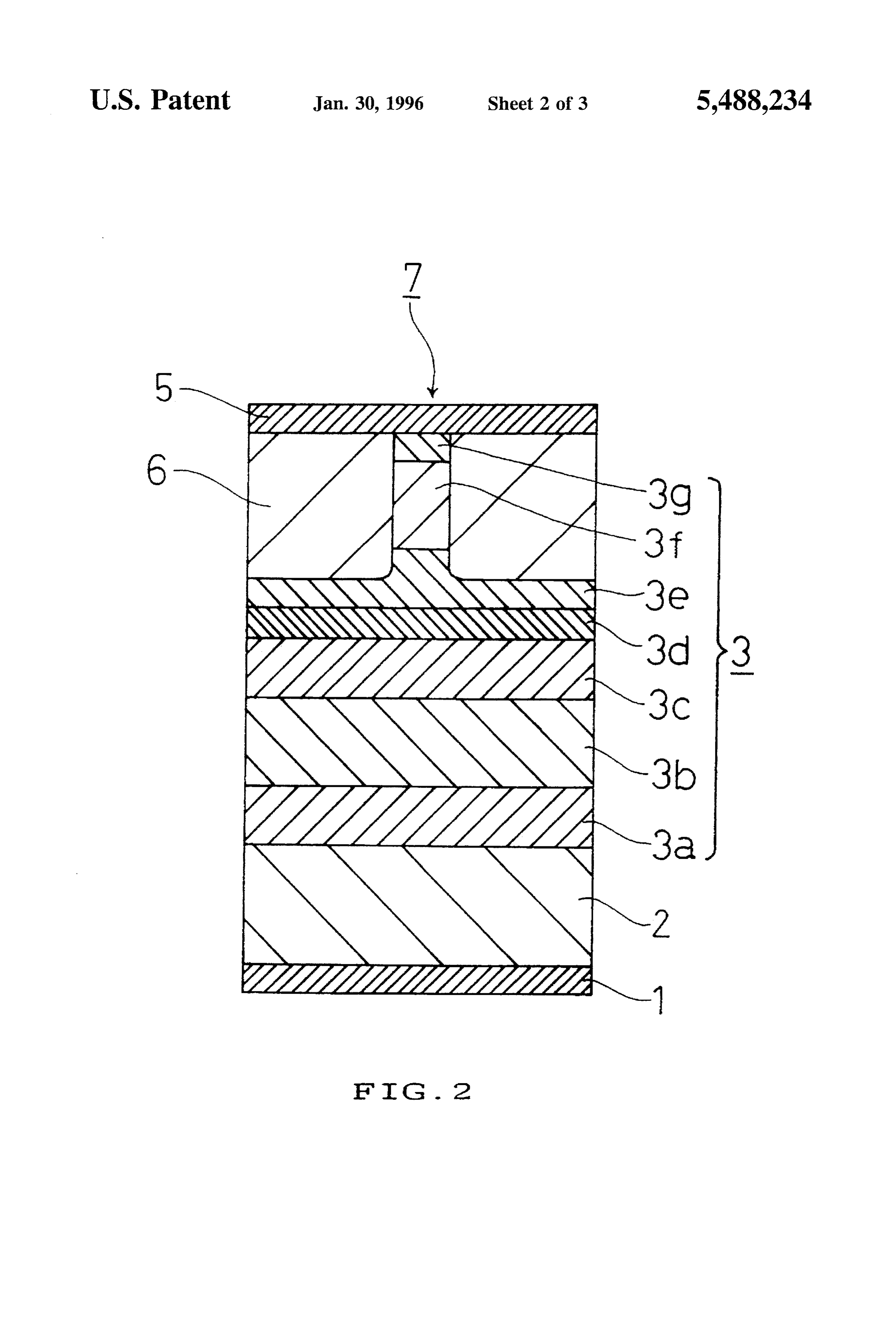
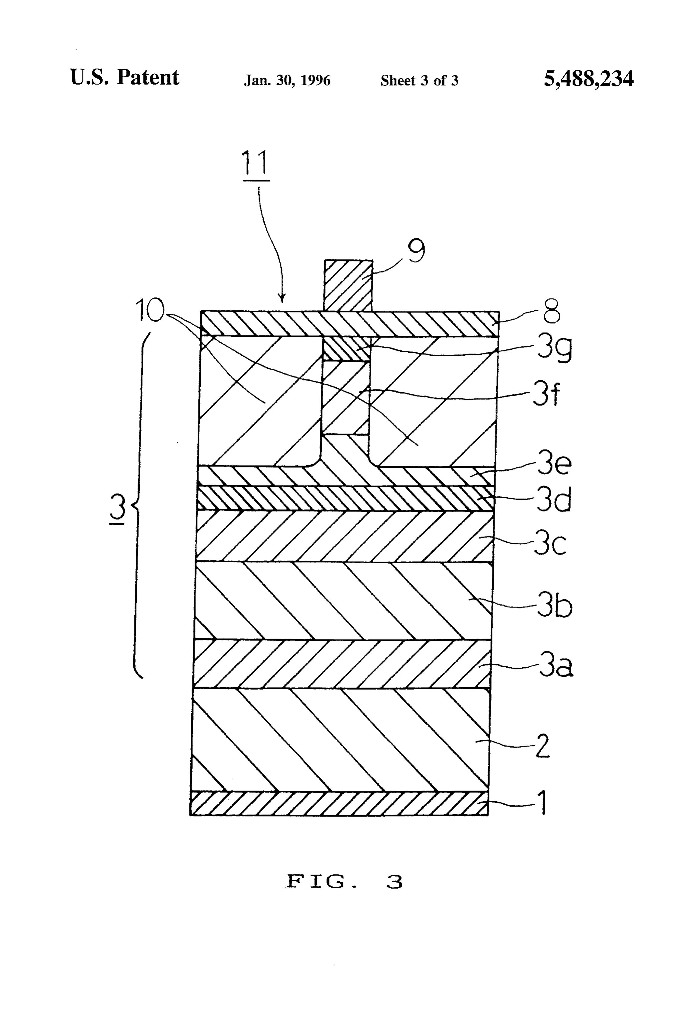
FIG. 2 shows a cross-sectional view of a semiconductor invention, most of the ions implanted from the surface of the laser of the embodiment of the invention after the implan metal electrode penetrate the electrode and the II-VI group tation of ions. semiconductor, thus making the penetrated area of the II-VI FIG. 3 shows a cross-sectional view of a semiconductor group semiconductor highly resistant. laser of another embodiment of the invention. 10 However, ions irradiated to the surface of a metal section, which is set on the metal electrode, lose penetrating energy
DETAILED DESCRIPTION OF THE due to interactions with metal atoms of the metal section and INVENTION stop penetrating inside of the metal section without reaching
An insulating layer is formed in a II-VI group semicon 15 the metal electrode and the II-VI group semiconductor. ductor by implanting ions to the n-type or p-type II-VI Thus, the metal section is used as a mask against the group semiconductor layers in an amount from 10°-10 implantation of ions, and the area right below the metal ions/cm, thus manufacturing a II-VI group semiconductor section has little resistance.
element which comprises an insulating layer having good In other words, no electric current transmits through the thermal contacts with semiconductor materials and sufficient 20 area of the II-VI group semiconductor where ions are thermal conductivities. implanted (insulating layer or current blocking area) while When the energy of incident ions is low, the reflection the current is confined and flows only through the area right below the metal section.
and/or accumulation of ions, the sputtering of surface atoms or the like is generated by the process of implanting ions to In the semiconductor laser element of the invention, the a II-VI group semiconductor. Sufficiently accelerated ions, 25 insulating layer is sufficiently close to an active layer, thus on the other hand, penetrate the inside of the II-VI group efficiently confining the electric current. Thus, current den semiconductor, and lose energy due to interactions with sity at the active layer is high, and the threshold current atomic nuclei of the semiconductor (nucleus collision) or required for a laser oscillation is low. The operating voltage with electrons (electron collision). As a result, ions stop required for obtaining a certain level of laser output is also penetrating at a certain depth of the semiconductor. 30 lowered by this semiconductor laser element. Atoms of the semiconductor are displaced from the lattice When the semiconductor laser element is fixed on a heat positions due to the nucleus collision between incidentions sink (radiator), thermal contacts between the heating area of and the atoms. Displaced atoms then knock off other atoms, the element and the heat sink improve by applying the metal thereby generating lattice defects including interstitial atoms section having high thermal conductivity on the top of the and vacant lattice points. Dislocations and/or voids are then 35 heating area.
generated. Therefore, the semiconductor laser element of the inven Since carriers inside the semiconductor are reflected and tion has good radiating properties and endurance. scattered by these lattice defects, dislocations or the like, the Since the insulator of the invention is manufactured by mobility of carriers is lowered. As a result, since the electric implanting ions in an amount from 10° to 10 cm ions/’ to conductivity at the area where ions are implanted decreases 40 an n-type or p-type semiconductor, it increases thermal considerably, the area has high resistance and is employed as contacts with semiconductor materials and improves ther a useful insulating layer. mal conductivity.
Heat generated in the semiconductor element is diffused The insulating layer of the invention is useful for semi by lattice vibrations. However, if the lattice constants of the 45 conductor laser elements, light emitting diode elements, IC, insulating layer and n-type (or p-type) layer are not adjusted LSI and the like. The insulating layer is particularly useful and/or if there is no continuous interface between the since it diffuses heat generated inside the semiconductor to insulating layer and the n-type (or p-type) layer, lattice the outside.
vibrations are scattered and reflected at the interface. Thus, For a semiconductor, it is preferable to use a compound of a preferable level of thermal contacts between the insulating 50 at least one bivalent element selected from the group con layer and the n- (or p-type) layer cannot be obtained. sisting of Zn, Cd, Mg, Mn, Hg and Ca and at least one VI According to the method of manufacturing an insulating group element selected from the group consisting of S, Se layer of the invention, however, there is no clear interface and Te. Such a semiconductor (for example, ZnCd. between the insulating layer and the p-type (or n-type) layer. xSySe1-y, ZnxCd1-xSySe1-y, ZnxMg1-S-Se-y or ZnxMn As a result, lattice vibrations are directly diffused from the 55 xSSe (wherein 0sXs 1 and 0s Ys 1)) can vary the n-type (or p-type) layer to the insulator, thus providing lattice constants within the range of 0.53-0.67 nm. As a superior thermal contacts between the insulating layer and result, the lattice constant can be adjusted to the lattice the p-type (or n-type) layer. constant of the n-type (or p-type) layer of the semiconductor Since the thermal conductivity of the insulating layer of laser element.
the invention is higher than that of SiO, or polyimide resins, 60 This semiconductor can arrange the band gap in a range the insulating layer releases heat received from the semi of 0-4.2 eV, and its conduction type can also be easily conductor to the outside of the semiconductor element at a controlled by adding p type and n type impurities to the higher speed. Semiconductor.
The semiconductor laser element comprising the insulat It is preferable to use ions of I group or V group elements ing layer of the invention has lower calorific power than a 65 Such as hydrogen, nitrogen, lithium, phosphorus and the like conventional semiconductor laser element comprising SiO, as incidentions to an n-type semiconductor. Ions of I group or polyimide resins as an insulating layer. The insulating or V group elements generate acceptor levels in the n-type
Page 7
Semiconductor. The ions, at the same time, compensate Light absorption from the defects in the semiconductor electrons (carriers) inside the semiconductor and reduce the implanted with ions is small enough that the semiconductor density of the electrons. As a result, it is possible to does not require a heat treatment. Even if the heat treatment manufacture an insulating layer with high resistance by is carried out on the semiconductor after the implantation of irradiating ions at a relatively low dose, and to improve the ions, the crystallinity of the semiconductor can be recovered thermal conductivity of the insulating layer by reducing the by a heat treatment of 100°-400° C. This is because the damage to the crystals of the insulating layer. ionicity of the semiconductor is high, and the atoms are For these reasons, it is preferable to use ions of III group mobile. Therefore, the insulating layer can be easily formed or VII group elements generating donor levels such as in the semiconductor layers without damaging them with chlorine, gallium, fluorine, bromine and the like as incident 10 heat.
ions to a p-type semiconductor.
In addition, nitrogen and phosphorus ions can also be used as incident ions, since the implanted ions in the semicon EXAMPLE 1. ductor layers do not diffuse to the area immediately below A 1.8 pum thick ZnSethin film (single-crystal II-VI group the metal section where the ions are not implanted. 15
When the substrate temperature during the implantation semiconductor) was formed on a GaAs substrate by a of ions is 0-300° C., there is no damage to the semicon molecular beam epitaxial growth (MBE) method at ductor except the area where the ions are implanted. The 200°–400° C. growth temperature and 1x10Torr vacuum. insulating layer of the semiconductor, in addition, achieves By adding chlorine at 2x10 cm during the film growth, a stable resistivity. 20 the ZnSe thin film became n-type. The resistivity of the
If the ion beam current density during the implantation of n-type ZnSe thin film was 0.08 C2.cm. ions is 10 nA/cm°-1 uA/cm, no damage is provided to the Hydrogen ions accelerated with 350 keV acceleration semiconductor except the area where the ions are implanted. voltage were implanted to the n-type ZnSe thin film. The Moreover, the insulating layer of the semiconductor can be incident angle of ions was 7, and the dose was 1x10' formed efficiently. 25 ions/cm'. The current density was 23 nA/cm and the The acceleration voltage of ions is preferably from 10 keV substrate temperature as 100° C. Due to the implantation of to 1000 keV. Ions accelerated at this range of voltage can the ions, the resistivity of the n-type ZnSe thin film became easily penetrate the semiconductor. As a result, surface higher than 1x10 G2.cm. Based on this level of resistance, atoms are not sputtered, and there is no nucleus collision the n-type ZnSethin film can be used as an insulating layer between the ions and the atoms of the semiconductor. of a semiconductor element.
The thickness of the insulating layer is controlled by The principles of providing a practical level of resistance arranging the acceleration voltage of incident ions. For are as follows. Accelerated ions penetrate the inside of the instance, when nitrogen ions are implanted to the ZnSe of II-VI group semiconductor, and lose energy due to the the semiconductor, the insulating layer with a thickness of interactions with atomic nuclei of the semiconductor 10 nm-10 um is manufactured by changing the accelerating 35 (nucleus collision) or with electrons (electron collision). As voltage in the range of 10–1000 keV. However, it is difficult a result, ions stop penetrating at a certain depth of the to determine the exact thickness of the insulating layer since semiconductor.
there is no clear interface between the insulating layer and Atoms of the semiconductor are displaced from the lattice the semiconductor in the invention.
positions
Gold having a good thermal conductivity and electric 40 and the atoms. due to the nucleus collision between incident ions conductivity can be used for the metal section of the Displaced atoms then knock off other atoms, Semiconductor element. In addition, since gold has a large thereby generating lattice defects including interstitial atoms atomic weight, it can efficiently stop the ions from penetrat and vacant lattice points. Dislocation or void is then gener 1ng. ated by shifting and combining the lattice defects. Since If nitrogen ions accelerated to 10-1000 keV are used as 45 carriers by these inside the semiconductor are reflected and Scattered lattice defects, dislocations or the like, the mobility implanted ions, and gold is used as the metal section, the of carriers is lowered. As a result, since the electric conduc ions can be efficiently stopped from penetrating the metal tivity at the area where ions are implanted decreases con section by setting the thickness of the section at 0.1-10 um. siderably, the area has high resistance and becomes useful as In the invention, it is possible to form the insulating layer a good insulating layer.
sufficiently close to the active layer as a current blocking 50 The thermal conductivity of the insulating layer of this layer. Since the active layer is also surrounded with the example was 15 W/m-k while the thermal conductivities of insulating layer, an n-type semiconductor can be applied a conventional SiO2 insulating layer and of a polyimide above the active layer without scattering electric current. resin insulating layer were 1.4 W/m-k and 0.3 W/m-k The insulating layer has preferable ohmic contacts particu respectively.
larly with n-type Semiconductors, and metal electrodes with 55 low contact resistance can be used as a top electrode. Thus, the operating voltage of the semiconductor element as well EXAMPLE 2 as the generation of heat at the top electrode can be reduced.
When a p-type semiconductor is applied above the active AII-VI group semiconductor laser element as shown in layer, the insulating layer of the invention can more effi 60 FIG. 1 was manufactured as follows:
ciently confine electric current than conventional insulating forming a ZnSe base SQW-SCH (single-quantum-well layers. Therefore, current density in the active layer is separate-confinement-heterostructure) 3 on the surface improved, and the threshold current of the element is of a p-type GaAs substrate 2 by an MBE method; reduced. forming a mask 4 on the surface of the ZnSe base The invention is now specifically explained by referring 65 SOW-SCH3; and to the following examples. The examples are illustrative and depositing a metal electrode 1 on the bottom surface of the should not be construed as limiting the invention in any way. p-type GaAs substrate 2.
Page 8
Mask 4 is to prevent the penetration of irradiated ions, The semiconductor treated with heat at 300° C. for five thus forming an area of low resistance inside the semicon minutes after the implantation of ions exhibited the same ductor right below the mask. characteristics as the semiconductor with no heat treatment. Nitrogen ions were irradiated to the top surface of the The structures of the semiconductor laser element of the II-VI group semiconductor laser element shown in FIG. 1 invention include not only a single-quantum-well separate with 350 keV acceleration voltage. The incident angle of confinement-heterostructure but a buried-heterostructure ions was 7°, and the dose of the ions was 1x10' ions/cm. and a multiple quantum well structure.
Except for the area in the semiconductor right below mask 4, nitrogen ions were implanted. As a result, as shown in EXAMPLE 3
FIG. 2, a current blocking layer (insulating layer) 6 was O formed. Then, mask 4 was removed, and a metal electrode AII-VI group semiconductor element as shown in FIG. 5 was deposited on current blocking layer 6. Thus, a 3 was manufactured as follows. A ZnSe base SQW-SCH 3 semiconductor laser element 7 shown in FIG. 2 was manu was formed on the surface of a p-type GaAs substrate 2 by factured. In FIGS. 1-2, 3a and 3c indicate p-type ZnSe an MBE method, and a metal electrode 8 was formed on layers; 3b is a p-type ZnSSe layer; 3d is a ZnCdSe active ZnSe base SQW-SCH3. A titanium layer and a gold layer layer; 3e and 3g indicate n-type ZnSe layers; and 3f is an 15 were deposited by an electron beam and laminated on ZnSe n-type ZnSSe layer. base SQW-SCH 3, thus forming metal electrode 8 at a Semiconductor laser element 7 had 520 nm wavelength, thickness of 30 nm. Then, gold electrolytic plating was and oscillated at 360 mA threshold current and 33 V element directed on the laminated layers, thus forming a 10 um wide Voltage.
As a comparison, a semiconductor laser element, which 20 and 3pm thick striped metal section 9 on metal electrode 8.
A metal electrode 1 was formed on the bottom surface of the had the same laser structure, stripe shape and oscillating Substrate.
wavelength as semiconductor laser element 7 but had a conventional insulating-layer such as SiO2, polyimide or the Nitrogen ions accelerated at 350 keV acceleration voltage like, oscillated at 930 mA threshold current and 39 V were implanted by irradiation through the top surface of the element voltage. 25 II-VI group semiconductor element. The incident angle of In other words, by applying current blocking layer 6 the ions was 7, and the dose was 1x10' ions/cm. instead of a conventional insulating layer to an n-type II-VI A current blocking layer (insulating layer) 10 with high group semiconductor, the threshold current can be reduced resistance was formed in the II-VI group semiconductor by by 570 mA. Therefore, the element of the invention had implanting ions.
three times more element efficiency at 1 mW output than the 30 However, ions implanted to metal section 9 lost energy conventional element; it also reduced the caloric power to and stopped inside of metal section 9 due to the interaction less than one third of the caloric power of the conventional between the ions and the metal atoms. Thus, the area right element. below metal section 9 did not achieve resistance. Heat generated inside the semiconductor element is dif A 10 um thicklayer of gold was plated on the II-VI group fused by lattice vibrations. However, if the lattice constants 35 semiconductor element by electrolytic plating. The element of the insulating layer and the n-type (p-type) layer are not was then fixed on a radiator to evaluate the characteristics of matched or if there is no continuous interface between the the element.
insulating layer and the n-type (p-type) layer, lattice vibra According to the evaluation, semiconductor laser element tions are scattered and/or reflected at the interface. Thus, 11 of the example had lower calorific power and better preferable thermal contacts between the insulating layer and 40 radiating properties than a conventional semiconductor laser the n-type (p-type) layer cannot be obtained. element having SiO, or polyimide insulating layer. Thus, the In the method of forming current blocking layer 6, life span of semiconductor laser element was from 2 to 7 implanted ions are randomly scattered and stopped inside times longer than that of the conventional semiconductor the II-VI group semiconductor. The resistivity of the current blocking layer increases as the quantity of implanted ions 45 laser element.
increases. There is no clear interface between the current Even though a heat treatment after the implantation of blocking layer and the p-type (or n-type) semiconductor. ions is not carried out in the examples of the invention, a Therefore, the lattice vibrations can directly spread from the heat treatment of 100-400° C. can be directed to a semi n-type (or p-type) layers to current blocking layer 6, thus conductor in order to reduce crystal damages as well as the providing preferable thermal contacts between the n-type (or 50 light abosorption of the semiconductor layers. p-type) layers and the current blocking layer. The thermal In this example, the insulating layer was formed in the conductivity of current blocking layer 6 is higher than that area above the active layer. However, by increasing the of the conventional insulating layer such as SiO, or poly acceleration voltage of implanted ions, the insulating layer imide resins. Therefore, current blocking layer 6 can release can be formed down to the area below the active layer. the heat generated in the semiconductor element at high 55 The invention may be embodied in other specific forms speed. without departing from the spirit or essential characteristics Semiconductor laser element 7 comprising current block thereof. The embodiments disclosed in this application are to ing layer 6 has less calorific power and better radiating be considered in all respects as illustrative and not restric properties than the laser element comprising the conven tive, the scope of the invention being indicated by the tional insulating layer. Thus, the life span of semiconductor 60 appended claims rather than by the foregoing description, laser element 7 is 1.5-5 times longer than that of the and all changes which come within the meaning and range conventional semiconductor laser element. of equivalency of the claims are intended to be embraced Current blocking layer 6 shown in FIG. 2 is formed down therein.
to the area above ZnCdSe active layer 3d. However, if the We claim:
acceleration voltage of implanted ions is increased, current 65 1. A semiconductor element comprising a compound of at blocking layer 6 can be formed down to the area below least one bivalent element and at least one VI group element, ZnCdSe active layer 3d. wherein said semiconductor element has an insulating layer,
Page 9
Said insulating layer comprising ions implanted on at least metal section is insulated by the implantation of ions, thus one n-type semiconductor layer of the semiconductor ele forming an insulating layer.
ment in an amount from 10° ions/cm' to 10 ions/cm, 7. A semiconductor element according to claim 6, wherein wherein said implanted ions are at least one element selected the metal section, formed partially on the metal electrode, from the group the consisting of I group and V group. comprises laminated metal layers which form stripes on said 2. A Semiconductor element according to claim 1, wherein metal electrode.
the insulating layer has a thickness from 10 nm to 10 um. 8. A semiconductor element according to claim 6, wherein 3. A semiconductor element according to claim 1, wherein the metal electrode has a thickness from 10 nm to 1 um. a compound of at least one bivalent element selected from 9. A semiconductor element according to claim 6, wherein the group consisting of Zn, Cd, Mg, Mn, Hg and Ca and at 10 least one VI group element selected from the group consist the metal section has a thickness from 0.1 um to 10 um. ing of S, Se and Te is used for said semiconductor element. 10. A semiconductor element comprising a compound of 4. A Semiconductor element according to claim 1, wherein at least one bivalent element and at least one VI group the Semiconductor element is a semiconductor laser element. element, wherein said semiconductor element has an insu 5. A semiconductor element according to claim 4, wherein lating layer, said insulating layer comprising ions implanted the insulating layer is a current blocking layer. on at least one p-type semiconductor layer of the semicon 6. A semiconductor element according to claim 4, wherein ductor element in an amount from 10’’ ions/cm to 10' the semiconductor element comprises a semiconductor hav ions/cm', wherein said implanted ions are at least one ing a multilayer structure on a substrate, a metal electrodeelement selected from the group consisting of III group and formed on one entire surface of said semiconductor and a 20 VII group element ions.
metal section formed partially on said metal electrode, and wherein said semiconductor except the area right below said
Provenance
- Collection
- Cited prior art
- Original PDF
- patentimages.storage.googleapis.com →
- Filed
- 1994-03-17
- Pages
- 9
- Method
- pdftotext (the PDF's own text layer) + pdftoppm 300dpi page scans
- Source
- Google Patents bibliographic record
- Granted
- 1996-01-30
- Inventors
- Shigeo Yoshii; Kazuhiro Okawa; Ayumi Tsujimura; Tsuneo Mitsuyu; Matsushita Electric Industrial Co Ltd
- Transcribed from
- patentimages.storage.googleapis.com →