patent · US5643423
Method for producing an abrasion resistant coated substrate product
1 July 1997
Page 1 — bibliographic record
United States Patent (19) 11 Patent Number: 5,643,423 Kimock et al. 45 Date of Patent: Jul. 1, 1997 54 METHOD FOR PRODUCING ANABRASION 51-128686 11/1976 Japan. RESISTANT COATED SUBSTRATE 59-26906 2/1984 Japan.
PRODUCT 63-1952.66 8/1988 Japan.
75 Inventors: Fred M. Kimock, Macungie; Bradley 63-22184 9/1988 Japan.
J. Knapp; Steven James Finke, both 1-147O67 6/1989 Japan.
of Kutztown, all of Pa. 1-147O68 6/1989 Japan.
73 Assignee: Monsanto Company, St. Louis, Mo.
OTHER PUBLICATIONS
21 Appl. No.: 161,896 Bubenzer, et al., Proc. DARPA Workshop DLB Coat. (1982) 22 Filed: Dec. 3, 1993 issue date AD-A136766, 33-47, editor B. Bendow (no month available).
Related U.S. Application Data Stein, et al., NBS Spec. Publ. 638, 482-488 (1984) (no 60 Division of Ser. No. 924297, Aug. 3, 1992, Pat. No. month available).
5,268,217, which is a continuation-in-part of Ser. No. 589, Bubenzer, et al., NBS Spec. Publ. 638, 477-481 (1984) (no 447, Sep. 27, 1990, Pat. No. 5,135,808. month available).
(51) Int. Cla.m. C23C 14/00 Liou, et al., Appl. Phys. Lett., 55, 631-633 (1989) (no month 52 U.S. C. ................................ 204/19235; 204/192.36: available).
427/164; 427/166; 427/167; 427/249; 427/250; Franks, J. Vac. Sci. Technol, A7, 2307-2310 (1989) (no 427/255.7; 427/294; 427/299; 427/309; month available).
427/398.4; 427/534 Nir, Thin Solid Films, 144, 201-209 (1986) (no month (58) Field of Search .................................... 427/164, 166, available).
427/167,249,250, 255.7, 398.4, 299, 309, (List continued on next page.)
56 References Cited Primary Examiner-Bernard Pianalto Attorney, Agent, or Firm-Coudert Brothers
4,060,660 11/1977 Cardson et al. ... ... 427/39 4,383,728 5/1983 Litington ....... ... 350/1.7 The coated substrate product finds particular application in 4,400,410 8/1983 Green et al. .. 427/39 eyeglass and Sunglass lenses, architectural glass, analytical 4,504,519 3/1985 Zelez ............. ... 427/39 instrument windows, automotive windshields and laser bar 4,569,738 2/1986 Kieser et al. 204/173 code scanners for use in retail stores and supermarkets. The 4,603,082 7/1986 Zelez ....................................... 428/336 product has greatly improved wear resistance for severe 4,661409 4/1987 Kieser et al. . 428/408 4,746,538 5/1988 Mackowski ....... ... 427/38 abrasive environments and comprises a substantially opti 4,877,677 10/1989 Hirochi et al..... 428/26 cally transparent substrate, a chemically vapor deposited 4907,846 3/1990 Tustison et al. .. 350/1.6 first interlayer bonded to the substrate and a chemically 5,235,168 8/1993 Bobba ..................................... 235/462 vapor deposited outer layer of substantially optically trans FOREIGN PATENT DOCUMENTS parent diamond-like carbon bonded to the interlayer and 243451 5/1987 European Pat. Off.. away from the substrate.
42 01914A1 7/1992 Germany. 70 Claims, 2 Drawing Sheets
Page 2
OTHER PUBLICATIONS Final Program of American Vacuum Society 37th Annual Symposium in Toronto, Canada, cover & pp. 66-67 (Oct.
Deutchman, et al., Proc. SPIE Int. Soc. Opt. Eng. 1146, 8-12, 1990).
124-34 (1989) (no month available). Paper from aforementioned symposium: Saumel J. Holmes Collins, et al., Proc. SPIE Int. Soc. Opt. Eng. 1146, 37-47 and V. Warren Ciricik, "Optical Properties and Intrinsic (1989) (no month available). Coating Stresses In Ion Beam Sputter Deposited Silicon Liou, et al., Proc. SPIE Int. Soc. Opt. Eng. 1146, 12-20 (No Oxynitride Films”, Northrop Research and Technology Cen date). ter (Oct. 8, 1990).
Page 3
Drawing sheet — no readable text.
Page 4
Drawing sheet — no readable text.
Page 5
METHOD FOR PRODUCING AN ABRASION Many methods for depositing DLC have been RESISTANT COATED SUBSTRATE demonstrated, including radio frequency plasma deposition, PRODUCT ion beam sputter deposition from a carbon target, ion beam sputtered carbon with ion beam assist, direct ion beam this application is a division of application U.S. Ser. No. 5 deposition, sition from a dual ion beam deposition, laser ablation depo carbon target, and ion beam assisted evapora
issued Dec. 3, 1993 (Docket No. 52006), which patent is a tion of carbon. Many of these prior art techniques have been Continuation-in-Part of application U.S. Ser. No. 07/589, used to deposit DLC on glass substrates, however, the 447, filed Sep. 27, 1990, now U.S. Pat. No. 5,135,808, 10 DLC to theof glass emphasis the prior art has not been on the adhesion of the substrate or on the abrasion resistance of issued Aug. 4, 1992. the coated substrate product. Illustrative are the following FIELD OF THE INVENTION references: U.S. Pat. Nos. 4,746,538; 4400,410; 4.383,728;
This invention relates generally to coated substrate prod 4,661409; Japanese Patent Nos. 63/221841; 63/221840; ucts. More particularly, the invention relates to a substan 63/195266; 1147068; 1147067; 64-2001: 59-26906 and tially optically transparent coated substrate product com 15 51128686; European Patent Nos. DD-203903; SU1006402; prised of a parent substrate, one or more interlayers and a European Patent Application#EPO 243541 (WO87/02713); diamond-like carbon layer, and to a method for producing Deutchman, et al.; Proc. SPIE-Int. Soc. Opt. Eng.1146, SaC. 124-34, 1989; Collins, et at, Proc. SPIE-Int, Soc. Opt. Eng.
BACKGROUND OF THE INVENTION 20 1146, 12-20, 1989; Bubenzer, et al., Proc. DARPA Work shop Diamond-Like Carbon Coat, Meeting date 1982, Issue
The properties of glass make it an ideal substrate material AD-A136 766, 33-47, edited by B. Bendow in NBS Spec. for use in many applications. In particular, the combination Publ. 669, 249-54, 1984; NBS Spec. Publ. 638, 482–82, of optical transparency, with reasonable strength at a nomi 1984; Bubenzer, et al., NBS Spec. Publ. 638,477-81, 1984; nal cost, allows the widespread use of glass products. Glass, 25 Appl. Phys. Lett. 55, 631-3, 1989; J. Vac. Sci. Technol A7, however, does suffer from several limitations. Glass is not a 2307-10, 1989; and D. Nir, Thin Solid Films, 144, 201-9, particularly hard material, and consequently it abrades in 1986. These references do not however describe the use of many applications. Additionally, glass is chemically reactive transparent interlayers to improve the adhesion of the amor with many alkaline substances and with hydrofluoric acid. phous carbon coating to the substrate or substantially opti New applications and superior performance in existing 30 cally transparent DLC coatings with greatly improved wear applications could be thus realized for glass products if glass resistance for severe abrasive environments. were more abrasion resistant and less chemically reactive. SUMMARY OF THE INVENTION Examples of glass products which could benefit from This invention provides a coated substrate product with improved abrasion resistance include eyeglass and Sunglass superior lenses, architectural glass, analytical instrument windows, 35 reactivity.abrasion
More wear resistance and reduced chemical particularly, this invention provides a automotive windshields and laser bar code scanners for use diamond-like carbon coating to the surface of an optically in retail stores and supermarkets. transparent substrate which is highly adherent and exhibits Diamond-like carbon films (DLC) are well known in the greatly improved wear resistance for severe abrasive envi art and have been recognized as potential coatings to ronments. Still more particularly, this invention provides a enhance the abrasion resistance of various Substrate coated substrate withimproved ease of cleaning. This inven materials, including glass. The DLC coatings possess excel tion also provides a low cost and efficient process for lent optical properties and exhibit excellent resistance to producing a coated substrate product with Superior abrasion abrasion and chemical attack by various acids, including wear resistance.
hydrofluoric acid. However, it has been found that the DLC The disclosed abrasion wear resistant coated Substrate coatings will impart improved abrasion resistance to a 45 product substantially reduces or eliminates the disadvan substrate only if the adherence of the coating to the parent tages and shortcomings associated with the prior art tech Substrate is excellent. niques. The invention discloses a substantially optically The most obvious and common approach to coating the substrate, onecomposite transparent or more structure which comprises a parent intermediate layers and a diamond glass substrate is to apply the DLC coating directly onto a like carbon layer in which at least one of the intermediate clean glass surface. However, this approach often results in 50 layers has thickness in the range a DLC coating which displays poor adhesion and therefore, about 20 m. The invention alsoofdiscloses about 1 micron pum) to poor abrasion resistance. DLC coatings are typically under fabricating the coated substrate product. a method for significant compressive stress. This stress greatly affects the According to the method, the substrate surface is initially ability of the coating to remain adherent to the glass sub chemically de-greased. In the second step, the substrate strate. Additionally, glass often contains many alkali oxides 55 surface is bombarded with energetic gas ions to assist in the and other additives which can inhibit the bonding of the removal of residual hydrocarbons, as well as alkali metals SiO in the glass to the carbon atoms in the DLC coating. It and other additives. After the substrate surface has been is currently believed that the reaction between the SiO in sputter-etched, one or more interlayers are chemically vapor glass and the DLC is essential for the coating to exhibit deposited on the substrate, followed by the deposition of a excellent adhesion. Therefore, less obvious methods are diamond-like carbon layer. Once the requisite number of required to produce a glass substrate with a highly adherent interlayers and diamond-like carbon layers have been DLC coating which provides excellent abrasion resistance. deposited, the coated substrate is cooled and removed from In addition to glass substrates, many other optically the reactor.
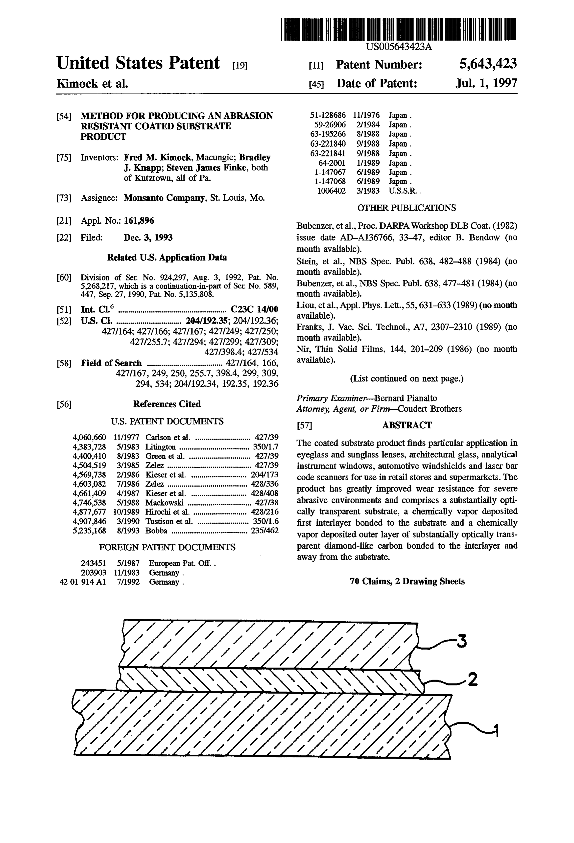
transparent substrate materials, such as sapphire, glassy BRIEF DESCRIPTION OF THE DRAWINGS ceramics, salts (NaCl, KBr, KCl, etc.), metal fluorides and 65 metal oxides could benefit from a DLC coating, but contain Further features and advantages will become apparent elements which inhibit the bonding of the DLC layer. from the following and more particular description of the
Page 6
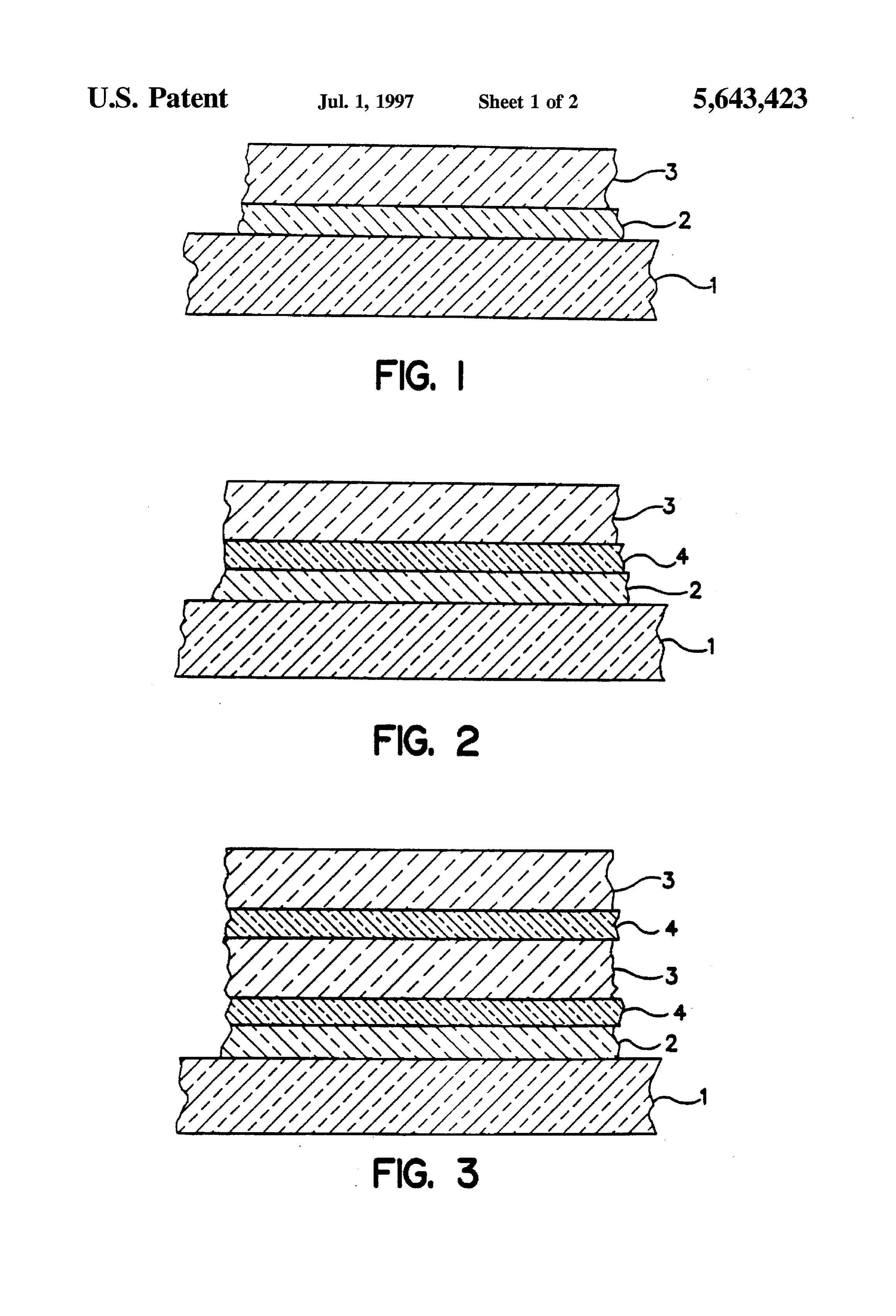
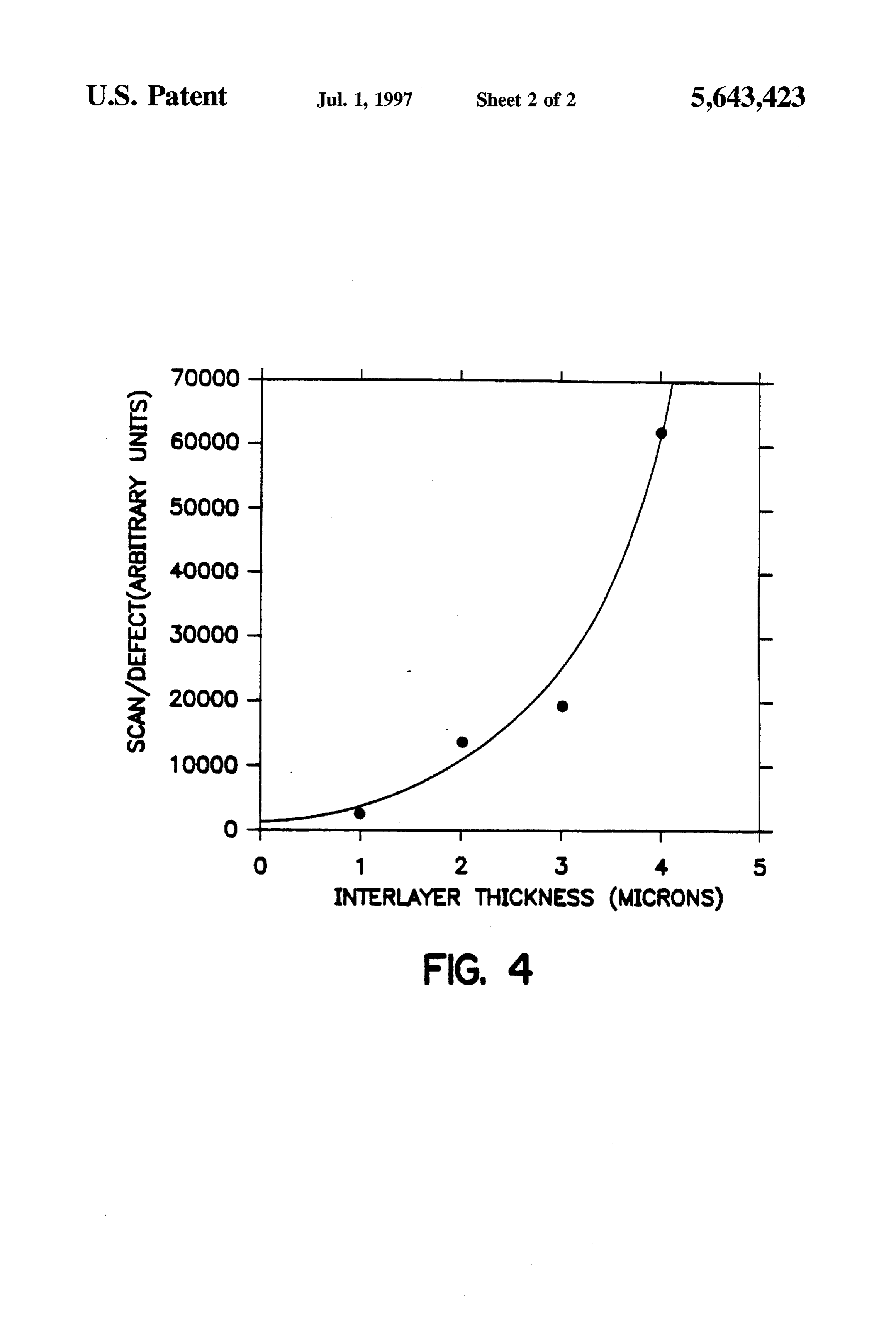
preferred embodiment of the invention, as illustrated in the the diamond-like carbon layer 3. Thus, the first interlayer 2 accompanying drawings, in which like reference characters must also have the property of providing a barrier to generally refer to the same parts or elements throughout the diffusion of alkali metals and additives from the parent views, and in which: substrate 1 to the diamond-like carbon layer 3. In the FIG. 1 is a cross-sectional view of the coated substrate preferred embodiment form of the invention, the first inter product in accordance with the present invention; layer comprises silicon nitride, titanium nitride, tantalum FIG. 2 is a cross-sectional view of the coated Substrate nitride, hafnium nitride, zirconium nitride, boron nitride, product in accordance with a further embodiment of the yttrium oxide, germanium oxide, hafnium oxide, silicon present invention; oxide, silicon dioxide, tantalum oxide, titanium oxide, Zir FIG. 3 is a cross-sectional view of the coated substrate 10 conium oxide, silicon carbide, germanium carbide, mixtures product in accordance with a still further embodiment of the thereof, and chemically bonded combinations thereof. By present invention; and the term "oxide", it is intended to mean a stoichiometrically FIG. 4 is a graph of the ratio of scans per defect versus the oxidized material, or a partially oxidized material which contains excess metal atoms, or is deficient in oxygen. By interlayer thickness of the coating of a coated bar-code 15 the term "nitride', it is intended to mean a material com scanner window product in accordance with the present posed of a stoichiometric amount of nitrogen or a material invention.
which either contains excess nitrogen atoms, or is deficient
DETAILED DESCRIPTION OF THE in nitrogen. By the term "carbide", it is intended to mean a INVENTION material composed of a stoichiometric amount of carbon or In accordance with the present invention, the disclosed adeficient material which either contains excess carbon atoms, or is
in carbon.
abrasion wear resistant coated substrate product substan tially reduces or eliminates the disadvantages and shortcom intended toterm
By the mean "chemically bonded combinations” it is a combination of at least two of the ings associated with the prior art techniques. As illustrated in FIGS. 1-3, the disclosed invention is a substantially 25 foregoing materials which are joined by chemical bonds, optically transparent composite structure which comprises a e.g. silicon oxide and silicon nitride to form silicon oxy parent substrate, one or more intermediate layers nitride.
(interlayers) and a diamond-like carbon layer. By the term of In the case of a single interlayer, first interlayer 2 rages "substantially optically transparent", it is intended to mean from approximately 1 um to 20 um in thickness. Preferably, transparent to light in the visible region of the electromag 30 the first interlayer 2 is from about 5 A thick to about 1 um netic spectrum, which is generally between 350 nanometers in those cases in which there are at least one otherinterlayer. and approximately 750 nanometers wavelength. A highly Following deposition of the first interlayer 2 onto the important technical advantage of the invention is that the parent substrate 1, the diamond-like carbon layer 3 is resultant multilayer composite structure produces a highly chemically vapor deposited onto the coated substrate. The abrasion wear resistant surface on various substrate 35 diamond-like carbon layer 3 can be from 10 A to 20 um in materials, particularly glass. thickness. Preferably, the diamond-like carbon layer 3 is at In the preferred embodiment form of the invention, as least 50 A thick.
illustrated in FIG. 1, a first interlayer 2 (or adhesion To further enhance the abrasion wear resistance of the mediating layer) is chemically vapor deposited onto a parent structure, more than one interlayer or a plurality of alter substrate 1 which comprises a substantially optically trans 40 nating interlayers and diamond-like carbon layers 3 may be parent amorphous material, a single crystal, polycrystalline deposited onto the parent substrate 1. It has been found that materials, glass, salt materials, ceramic materials and/or this arrangement allows for the deposition of a greater total mixtures thereof. By the term of "chemically vapor thickness of DLC material, which provides afurther increase deposited', it is intended to mean materials deposited by in abrasion resistance. Thus, in further envisioned embodi vacuum deposition processes, including thermal 45 ments of the invention, not shown, the structure may com evaporation, electron beam evaporation, magnetron prise a parent substrate 1, two different and separately sputtering, ion beam sputtering from solid precursor mate deposited first interlayers 2 and a diamond-like carbon layer rials; thermally-activated deposition from reactive gaseous 3; or a parent substrate 1 and two or more pairs of first precursor materials; glow discharge, plasma, or ion beam interlayers 2 and diamond-like carbon layers 3. deposition from gaseous precursor materials. Preferably, the 50 It has unexpectedly been found that in severe wear first interlayer 2 is deposited onto the parent substrate 1 by environments, the abrasion resistance of the coated Substrate ion beam or magnetron sputtering. product can be dramatically improved by using a relatively Atmospheric pressure deposition methods including arc thick, e.g. in the range of about 1 pm to about 20 pum, first spray or plasma-spray deposition from gaseous or solid interlayer 2 between parent substrate 1 and DLC layer 3. precursor materials, or thermally-activated deposition from 55 Such a highly abrasion wear resistant and corrosion resistant reactive gaseous precursor materials may additionally be coated substrate product is obtained by depositing such a employed to deposit the first interlayer 2. relatively thick film of at least one interlayer 2 having a The first interlayer 2 generally comprises a substantially hardness greater than that of substrate 1 and then depositing optically transparent material devoid of alkali metal atoms a comparatively thin, e.g. at least 50 A, layer of DLC as the and fluorine, and capable of forming a strong chemical bond top coat. In addition to serving as the bonding layers to the substrate 1 and the diamond-like carbon layer 3. By between substrate 1 and DLC top layer 3, interlayer(s) 2 the term of "strong chemical bond", it is intended to mean provide a hard "structural support layer” for DLC layer 3. that the interlayer is composed of a significant amount of an The thinner DLC top most layer provides a low friction, element or elements which are capable of undergoing a corrosion-resistant, protective surface for the substrate. The chemical reaction with carbon to form carbide-bonding. The 65 resulting coated substrate product has greater commercial absence of alkali metals and fluorine is essential to achieve utility than similar products in which the substrate is depos a highly adherent interface between the first interlayer 2 and ited with thin interlayer(s) 2 followed by a relatively thick
Page 7
DLC layer 3 in the following two cases. The first case is if provide a diffusion barrier to alkalimetal atoms and fluorine, the optical absorption coefficient of DLC layer 3 is too high they will not form a strong carbide bond with the diamond to allow a thick DLC layer to be deposited while simulta like carbon layer 3. Therefore, if any of these second group neously meeting stringent optical transparency requirements metallic materials are selected for the second interlayer 4, a for the coated product. The second case is if the deposition third interlayer (not shown) must be disposed between the rate of DLC layer 3 is much lower than that of interlayer(s) second interlayer 4 and the diamond-like carbon layer3. The 2, using a thick interlayer 2 to achieve the required degree third interlayer would similarly comprise a substantially of abrasion resistance is more economical than using a thick optically transparent material devoid of alkali metal atoms DLC layer 3. and fluorine and selected from the group consisting of In another embodiment of the invention, as illustrated in 10 silicon nitride, titanium nitride, tantalum nitride, hafnium FIG. 2, a second interlayer 4 is chemically vapor deposited nitride, zirconium nitride, boron nitride, yttrium oxide, gera onto the coated substrate and positioned such that the second nium oxide, hafnium oxide, silicon oxide, silicon dioxide, interlayer 4 is disposed between the first interlayer 2 and the tantalum oxide, titanium oxide, zirconium oxide, silicon diamond-like carbon layer 3. The second interlayer 4 would 15 carbide, geranium carbide, mixtures thereof, and chemically similarly comprise a substantially optically transparent bonded combinations thereof. Although it is not necessary, material devoid of alkali metal atoms and fluorine, and this third interlayer may be employed with the aforemen capable of forming a strong chemical bond to the first tioned first group of metallic materials.
interlayer 2 and the diamond-like carbon layer 3. The second The metallic second interlayer 4 can be from 5 A to 1000 interlayer may comprise a substantially optically transparent A in thickness. Preferably, the metallic second interlayer 4 silicon nitride, titanium nitride, tantalum nitride, hafnium 20 is at least 10 A thick.
nitride, zirconium nitride, boron nitride, yttrium oxide, ger In yet another embodiment of the invention, as illustrated manium oxide, hafnium oxide, silicon oxide, silicon in FIG. 3, the embodiment illustrated in FIG. 2 and dis dioxide, tantalum oxide, titanium oxide, Zirconium oxide, cussed above is provided with a second composite layer silicon carbide, germanium carbide, mixtures thereof, and 25 comprising a first interlayer 2 and a diamond-like carbon chemically bonded combinations thereof. layer 3. The resultant multilayer structure would thus be a Since the second interlayer 4 provides a diffusion barrier parent substrate 1, a first interlayer 2, a second interlayer 4, for alkali metal atoms, fluorine and/or any additional addi a diamond-like carbon layer 3, a first interlayer 2 and a tives which would adversely effect the adherence of the diamond-like carbon layer3. The structure may alternatively diamond-like carbon layer 3, the first interlayer could further 30 comprise a parent substrate 1, two first interlayers 2, a comprise a substantially optically transparent aluminum diamond-like carbon layer 3, a first interlayer 2 and a oxide, cerium oxide, tin oxide, thorium oxide, lithium oxide, diamond-like carbon layer.
sodium oxide, potassium oxide, rubidium oxide, cesium By choosing the appropriate interlayer 2, 4 and diamond oxide, francium oxide, beryllium oxide, magnesium oxide, like carbon layer 3 thicknesses, criteria which are known in calcium oxide, strontium oxide, cerium oxide, radium oxide, the art of optical coating design could be employed in each barium fluoride, cerium fluoride, magnesium fluoride, tho 35 of the aforementioned embodiments of the present invention rium fluoride, calcium fluoride, neodymium fluoride, lead to produce quarter wavelength stacks and other "dielectric fluoride, sodium fluoride, lithium fluoride, zinc selenide, stack" coating configurations. In these dielectric stack zinc sulfide, mixtures thereof, and chemically bonded com configurations, optical interference effects could be used to binations thereof. produce wavelength-selective mirrors or anti-reflection The second interlayer 4 can be from 5 A to 20 lm in films. By choosing the appropriate thickness of at least one thickness. Preferably, second interlayer 4 is at least 10 A of the interlayers 2, 4 and diamond-like carbon layer 3, the thick. Still more preferably, second interlayer 4 has a thick reflection of light at predetermined wavelength ranges may ness in the range of 1 um to 20 m in the case in which the be either minimized or maximized. Superior abrasion wear thickness of first interlayer(s) 2 is in the 5A to 1 m range 45 resistance and environmental durability currently unavail to achieve the unexpected results of greatly improved abra able with conventional optical coatings could thus be real sion resistance in severe wear environments for the coated ized by the incorporation of the dielectric stack configura substrate product. tions into the present invention. The second interlayer 4 may alternatively comprise a The method of the present invention teaches those skilled substantially optically transparent metallic material capable 50 in the art how to fabricate the transparent abrasion wear of reflecting visible light and capable of forming a strong resistant coated substrate product. According to the method, chemical bond with the first interlayer 2 and the diamond the first step involves chemically de-greasing the surface of like carbon layer 3, selected from the following two groups. the parent substrate 1. The substrate 1 is then placed into a In the first group, the metallic material may consist of chemical vapor deposition reactor vacuum chamber and the silicon, germanium, hafnium, molybdenum, tungsten, 55 air evacuated from the chamber to less than approximately yttrium, tantalum, titanium and zirconium. These metallic 5X10 Torr.
materials all form a strong chemical bond to the diamond In the next step the surface of the substrate 1 is sputter like carbon layer 3. etched with energetic ions or atoms to assist in the removal The second group of metallic materials comprises of residual hydrocarbons, as well as alkalimetals and other vanadium, niobium, chromium, manganese, then lure, additives which are commonly present on the surface of the technetium, iron, cobalt, iridium, rhodium, nickel, substrate materials, particularly glass. It has been found that palladium, platinum, copper, silver, gold, zinc, ruthenium, the concentration of alkali metals (Na,Ca) at the surface of indium, aluminum, tin, osmium, thallium, lead, antimony, glass substrates was significantly reduced as a function of bismuth and polonium. Among the second group of metallic ion sputter-etching time and that increased sputter-etching materials, rhenium, iridium, tin, indium, aluminum, nickel, 65 time substantially improved the adhesion of the diamond iron, chromium, copper, gold, silver and platinum are pref like carbon layer 3. See Examples A-Z). Therefore, it is erable as second interlayer 4. Although these materials will concluded that the removal of alkali metals and other
Page 8
additives is essential to achieve a highly adherent interface chamber which was then evacuated to 8x10⁷ Torr. The between parent Substrate 1 and the diamond like carbon sample was sputter-etched for 1 minute by a beam of Ar" layer 3. ions at an energy of 500 eV and a current density of 0.5 The sputter-etching may be performed with a beam of mA/cm'. The sample was then coated by direction beam inert gas ions, hydrogen ions or oxygen ions, a glow 5 deposition using an 11 cm ion beam source operated on CH discharge or a plasma of inert gas, hydrogen or oxygen. In gas at a pressure of 7.2x10 Torr. The ion energy was 75 eV the preferred embodiment form of the invention, sputter and the ion beam current density was 0.30 mA/cm. A etching is performed with a beam of energetic gas ions at an transparent coating of 3000 A thickness was deposited. The energy of at least 200 eV. sample was removed and scratch-tested by rubbing a sharp Following the sputter-etching step one or more interlayers 10 piece of glass or a glassjar across the interface between the are chemically vapor deposited onto the parent substrate 1. coated and uncoated (masked) areas. While the uncoated During a first cycle any of the aforementioned conventional area showed deep and wide scratches, no scratches were chemical vapor deposition methods may be employed to observed on the DLC-coated area. The coating was tested deposit the interlayers 2, 4 (FIG. 2 & 3). The deposition rate 15 for adhesion by alternately immersing the sample in baths of of each interlayer 24 is generally in the range of about boiling water (for 2 minutes) and ice water (for 2 minutes). 0.1-10 microns/hour. The total thickness of each interlayer After one thermal cycle, the coating peeled off of the glass Substrate.
can be in the range of about 5A to 20 um. In the preferred embodiment of the invention, the thickness of at least one EXAMPLEB interlayer is in the range of about 1pm to 20 Em and the total thickness for each of the other interlayers is at least 10 A. A 2"x2"x0.375" thick float glass plate was chemically After the chemical vapor deposition of one or more cleaned, mounted, masked, and ion sputter-etched in interlayers onto the parent substrate 1, a diamond-like car vacuum for 10 minutes by the procedure described in bon layer 3 is deposited onto the coated substrate. The Example A. Next, a 100-A thicklayer of SiO, was deposited diamond-like carbon layer 3 can be deposited by the fol 25 onto the glass plate by Arion beam sputter deposition from lowing conventional methods: (i) direct ion beam a quartz target. Then, a diamond-like carbon layer of 3,000 deposition, dual ion beam deposition, glow discharge, A thickness was deposited by the method described in RF-plasma, DC-plasma, or microwave plasma deposition Example A. The coating could not be scratched when rubbed from a carbon-containing gas or a carbon-containing vapor by a sharp piece of glass or a glassjar. The coating remained which can also be mixed with hydrogen, nitrogen-containing 30 adherent after 5 thermal cycles between boiling water and gases, oxygen containing gases and/or inert gas, (ii) electron ice Water.
beam evaporation, ion-assisted evaporation, magnetron sputtering, ion beam sputtering, or ion-assisted sputter depo EXAMPLE C sition from a solid carbon target material, or (iii) combina A 2"x2"x0.375" thick float glass plate was chemically tions of (i) and (ii). 35 cleaned, mounted, masked, and ion sputter- etched in In the preferred embodiment form of the invention, the diamond-like carbon layer(s) is deposited by ion beam vacuum by the procedure described in Example B. Next, a deposition from a hydrocarbon gas or carbon vapor. The ion plate by thick
layer of SiO, was deposited onto the glass ion beam sputter deposition from a quartz beam deposition may also be performed in combination with target. Then, a diamond-like carbon layer of 3,000 A thick an inert gas or hydrogen. ness was deposited by the method described in Example A. The deposition rate of the diamond-like carbon layer 3 is The coating could not be scratched when rubbed by a sharp generally in the range of about 0.1-10 microns/hour. The piece of glass or a glass jar. The coating remained adherent total thickness of the diamond-like carbon layer is generally after 5 thermal cycles between boiling water and ice water. in the range of about 10A to 20 um. Preferably, the thickness of the diamond-like carbon layer 3 is at least 50 A thick. 45 EXAMPLED After the deposition of the appropriate interlayers and diamond-like carbon layer(s) 3, as detailed in the aforemen A 2"x2"x0.375" thick float glass plate was chemically tioned embodiments. The coated substrate product is cooled vacuum bymounted, cleaned, masked, and ion sputter-etched in the procedure described in Example B. Next, the by extinguishing the deposition process and passing an inert gas over the substrate until it has reached substantially room 50 coating described in Example B was repeated three times in temperature. The coated substrate product, exhibiting supe sequence, so the total coating thickness deposited onto the rior abrasion wear resistance, is then removed from the glass plate was 9,300 A. The coating could not be scratched reactor. when rubbed by a sharp piece of glass or a glass jar. The The examples which follow illustrate the superior perfor coating remained adherent after 5 thermal cycles between mance of the invention. The examples are for illustrative 55 boiling water and ice water.
purposes only and are not meant to limit the scope of the EXAMPLEE claims in any way.
EXAMPLEA A 2"x2"x0.375" thick float glass plate was chemically cleaned, mounted, masked, and ion sputter-etched in
A 2"x2"x0.375" thick float glass plate was cut from a vacuum by the procedure described in Example A, except glass bar code scanner window and coated by the following the sputter-etching time was 5 minutes. Next, a 800 A thick procedure. The glass plate was chemically cleaned by layer of Al-O was deposited onto the glass plate by Arion beam sputter deposition from an aluminum oxide target.
trichloromethane followed by methanol solvents in an ultra
Sonic bath. The sample was removed and blown dry with Then, a diamond-like carbon layer of 200 A thickness was nitrogen gas. The glass plate was then mounted onto a 65 deposited by the method described in Example A. The Substrate holder and part of the substrate surface was coating could not be scratched when rubbed by a sharp piece masked. The sample was then inserted into a vacuum of glass. After 24 hours, the coating peeled off the substrate.
Page 9
EXAMPLE F Example A. The diamond-like carbon coating was very
A 1" diameterx0.06" thick soda lime glass disk was adherent, and could not be scratched with 50-micron quartz powder.
chemically cleaned, mounted, masked, and ion sputter etched in vacuum by the procedure described in Example A. EXAMPLEK Next, a 10,000A thicklayer of Al-O was deposited onto the glass plate by Ar" ion beam sputter deposition from an A 27 mm diameterx2 mm thick sapphire window was aluminum oxide target. Then, a 300-A thick layer of SiO, cleaned, mounted into a vacuum coating system, evacuated, was deposited over the Al-O layer by Arion beam sputter and sputter-etched for 1 minute using the conditions deposition from a quartz target. Next, a diamond-like carbon described in Example A. Then, a 50-A thicklayer of Siwas layer of 200 A thickness was deposited by the method 10 deposited onto the sapphire substrate by Art ion beam described in Example A. The coating could not be scratched sputter deposition from a Si target. Next, a transparent, when rubbed by a sharp piece of glass. After 5 thermal 1000-A thick layer of diamond-like carbon was deposited cycles between boiling water and ice water, the coating onto the sapphire substrate using the conditions described in remained adherent. 15
Example A. Subsequent optical spectroscopy analysis of the coating revealed that the Silayer had been converted into a
EXAMPLE G transparent layer of SiC by this process. The diamond-like A 6"x6"x0.375"thickfloat glass plate was initially coated carbon scratched coating was very adherent, and could not be with 50-micron quartz powder.
with about 2,000 A of SnO, by thermally activated depo sition from an organo-tin compound. The plate was then 20 EXAMPLEL chemically cleaned by the procedure described in Example
A, mounted, masked, and installed into a vacuum chamber A 130 mm diameterx1 mm thickaluminosilicate disk was which was then evacuated to 3.5x10Torr. The sample was mounted into a vacuum coating system, evacuated, and sputter-etched for 2 minutes by a beam of Ar" ions at an sputter-etched for 5 minutes, using the conditions described energy of 500 eV and a current density of 0.5 mA/cm. Next, 25 in Example A. Then, a 100-A thick layer of SiO, was a 1,000-A thick layer of SiO was deposited over the SnO2. deposited onto the aluminosilicate substrate using the con layer by Ar" ion beam sputter deposition from a quartz ditions described in Example B. Next, a 150-A thicklayer of target. Then, a diamond-like carbon layer of 2,000 A thick diamond-like carbon was deposited onto the aluminosilicate ness is deposited by the method described in Example A. substrate using the conditions described in Example A. The After 5thermal cycles between boiling water and ice water, 30 coating was very adherent, and could not be scratched with the coating remained adherent. a sharp piece of glass.
EXAMPLE H EXAMPLE M
A 6"x6"x0.375" thick float glass plate coated with about A 5.5"x5.5"x0.18" thick plate of Corning Code #9984 2,000 A of SnO, was chemically cleaned by the procedure 35 Pyroceramé (Note: Pyroceraméis a glass/ceramic material described in Example A, mounted, masked, and installed composed at least of rutile, aluminum oxide, and magnesium into a vacuum chamber which was then evacuated to 6x10 silicate.) was cleaned in isopropyl alcohol, blown dry with Torr. The sample was sputter-etched for 2 minutes by a beam nitrogen gas, mounted into a vacuum coating system, of Arions at an energy of 500 eV and a current density of evacuated, and sputter-etched for 15 minutes using the 0.5 mA/cm’. Then, a diamond-like carbon layer of 2,000 A conditions described in Example A. Then, a 200-A thick thickness was deposited by the method described in layer of SiO, was deposited onto the substrate as described Example A. During deposition, the DLC coating began to in Example B. Next, a transparent, 2000-A thick layer of peel off of the substrate, indicating poor adhesion. diamond-like carbon was deposited onto the substrate using
the conditions described in Example A. The coating was
EXAMPLE I very adherent, and could not be scratched by a sharp piece A 27 mm diameterx2 mm thick sapphire window was of glass.
ultrasonically cleaned in trichloromethane, followed by EXAMPLE N acetone, and then methanol, and blown dry with nitrogen gas. The Sapphire sample was mounted into the vacuum 50 A 5.5"x5.5"x0.18" thick plate of borosilicate glass was coating system and, after evacuation, sputter-etched for 3 cleaned in isopropyl alcohol, blown dry with nitrogen gas, minutes as described in Example A. Then, a 1000-A thick mounted into a vacuum coating system, evacuated, and layer of diamond-like carbon was deposited onto the sap sputter-etched for 15 minutes using the conditions described phire substrate using the conditions described in Example A. in Example A. Then, a 200-A thick layer of SiO, was A powdery carbon material was observed on the surface of 55 deposited onto the substrate as described in Example B. the substrate upon removal from the coating chamber indi Next, a transparent, 2000-A thick layer of diamond-like cating that the coating was not adherent. carbon was deposited onto the substrate using the conditions described in Example A. The coating was very adherent, and
EXAMPLEJ could not be scratched by a sharp piece of glass.
A 27 mm diameterx2 mm thick sapphire window was EXAMPLE O cleaned, mounted into a vacuum coating system, evacuated, and sputter-etched for 1 minute using the conditions A 2"x2"x4" thick piece float glass and a 70 mm described in Example A. Then, a 100-A thick layer of SiO, diameterx3 mm thick neutral gray glass sunglass lens were was deposited onto the sapphire substrate using the condi ultrasonically cleaned in isopropanol, and blown dry with tions described in Example B. Next, a transparent, 1000-A 65 nitrogen gas. The substrates were mounted into the vacuum thick layer of diamond-like carbon was deposited onto the coating system and, after evacuation, sputter-etched for 5 sapphire substrate using the conditions described in minutes as described in Example A. Then, a 100-A thick
Page 10
layer of SiO2 was deposited onto the substrates using the chamber. The vacuum chamber was then evacuated to a conditions described in Example B. Next, a 100-A thick pressure of 5X10 Torr. Next, the sample was sputter-etched layer of Siwas deposited on top of the SiO layer by Arion for 10 minutes with a beam of Ar" ions at an energy of 500 beam sputter deposition from a Sitarget. Finally, a 1,000-A eV and a current density of 0.5 mA/cm. A3000-A layer of thick layer of transparent diamond-like carbon was depos SiO was then deposited by ion beam sputter deposition by ited on top of the Silayer using the conditions described in bombarding a silica target with a beam of Nations. Next a Example A. The coating was very adherent, and could not be 1-micron layer of “silicon oxy-nitride” was deposited onto scratched with a sharp piece of glass which could easily the glass plate by bombarding a Sitarget with a beam of N' scratch the un-coated glass substrates. The coating on the ions in the presence of air. After deposition of the silicon sunglass lens exhibited an intense blue-purple reflected 10 oxy-nitride, a 100 A thicklayer of diamond-like carbon was color. deposited using a 11 cm ion beam source operated on
EXAMPLE P
methane gas at a pressure of 1.4x10'Torr. The beam energy was 75 eV and the beam current density was 0.3 mA/cm.
A 2"x2"X4 thick piece of float glass and a 70 mm 15 The coating was very adherent to the glass substrate. diameterx3 mm thick neutral gray glass Sunglass lens were EXAMPLES ultrasonically cleaned in isopropanol, and blown dry with nitrogen gas. The substrates were mounted into the vacuum A5.7"x5.7"x0.375" float glass substrate was cleaned and coating system and, after evacuation, sputter-etched for 5 mounted in a vacuum chamber as in Example R. The minutes as described in Example A. Then, a 100-A thick chamber was evacuated to a pressure of 5x10Torr. The layer of SiO, was deposited onto the substrates using the sample was ion beam sputter-etched as in Example R. Next, conditions described in Example B. Next, a 100-A thick a 3000-A SiO, layer was deposited as in Example R. Then, layer of Cr metal was deposited by Arf ion beam sputter a 2-micron silicon oxy-nitride layer silicon Oxy-nitride layer deposition from a Cr target. Next, a second 100-A thick was deposited as described in Example R. Finally, a 100-A layer of SiO, was deposited on top of the Cr layer. Finally, 25 DLC layer was deposited as in Example R. The coating was a 1,000-A thick layer of transparent diamond-like carbon very adherent to the glass substrate. was deposited on top of the SiO2 layer using the conditions described in Example A. The coating was very adherent, and EXAMPLET could not be scratched with a sharp piece of glass which A5.7"x5.7"x0.375" float glass substrate was cleaned and could easily scratch the un-coated glass substrates. The coating on the sunglass lens exhibited a brightblue reflected 30 mounted in a vacuum chamber as in Example R. The color. chamber was evacuated to 4x10Torr. The sample was ion beam sputter-etched as in Example R. Next, a 3000-A SiO,
EXAMPLE Q layer was deposited as in Example R. Then, a 3-micron silicon oxy-nitride layer was deposited as described in
An adherent, abrasion-resistant quarter-wavelength stack 35 Example R. Finally, a 100-A DLClayer was deposited as in reflecting coating was formed on glass substrates. The layer Example R. The coating was very adherent to the glass thicknesses were chosen to maximize reflectance at a wave substrate.
length of 450 nanometers. The refractive index of the deposited SiO2 layers was about 1.5, and the refractive index EXAMPLE U of the deposited DLC layers was about 2.05. The coating 40 was formed as follows: 5.7"x5.7"x0.375" float glass substrate was cleaned and A 2"x2"x4 thick piece of float glass and a 70 mm chamber wasmounted in a vacuum chamber as in Example R. The diameterx3 mm thick neutral gray glass sunglass lens were beam evacuated to 4x10Torr. The sample was ion ultrasonically cleaned in isopropanol, and blown dry with layer was depositedasasininExample
Example
R. Then, a 4-micron nitrogen gas. The substrates were mounted into the vacuum 45 coating system and, after evacuation, sputter-etched for 5 silicon oxy-nitride layer was deposited as described in minutes as described in Example A. Then, a 750-A thick Example R. The coating was very adherent to the asglassin Example R. A 100-A DLC layer was deposited layer of SiO, was deposited onto the substrates using the substrate.
conditions described in Example B. Next, a 555-A thick layer of transparent diamond-like carbon was deposited on 50 EXAMPLE V top of the first SiO, layer using the conditions described in
Example A. Next, a 750-Athicklayer of SiO, was deposited Four neutral gray tempered sunglass lenses were cleaned on top of the first DLC layer using the conditions described by the chemical cleaning procedure used in Example R. The in Example B. Finally, a 550-A thick layer of transparent lenses were Subsequently mounted onto a graphite plate. diamond-like carbon was deposited on top of the second 55 One-half of the surface was masked. The graphite plate was SiO2 layer using the conditions described in Example A. The then mounted in a vacuum chamber and the chamber was coating was very adherent, and could not be scratched with evacuated to 5X10 Torr. The lenses were Arion beam a sharp pie of glass which could easily scratch the un-coated sputter-etched as in Example R. Then, a 3000-A SiO, layer glass substrates. The coating exhibited a light yellow-blue was deposited as in Example R. Next a 0.5-micron silicon reflected color on the sunglass lens, and a lightblue reflected oxy-nitride layer was deposited as in Example R. Finally, a color on the glass plate. 200-ADLC layer was deposited as in Example R. The coating was very adherent to the sunglass lenses.
EXAMPLER
EXAMPLE W
A 5.7"x5.7"x0.375" soda-lime, float glass plate was cleaned with soap and water followed by rinsing with 65 Four tempered Sunglass lenses were cleaned, mounted, isopropanol and drying with nitrogen gas. The glass plate and masked as in Example V. The graphite plate was then was mounted onto a substrate holder which was in a vacuum mounted in a vacuum chamber and the chamber was evacu
Page 11
ated to 2x10Torr. The lenses were Ar" ion beam sputter Analogous results were obtained for a similar coating etched as in Example R.A3000A SiO, layer was deposited structure on glass sunglass lenses. Lenses were produced as in Example R. A 1 micron silicon oxy-nitride layer with silicon oxy-nitride interlayers of 0.5, 1, 2, 3 and 4 deposited as in Example R. A 200-A DLC layer was microns thickness (see Examples V-Z). These lenses were deposited as in Example R. The coating was very adherent 5 then scratched with #2 quartz particles under an applied to the sunglass lenses. pressure of 33 pounds per square inch. This test simulates
EXAMPLE X
severe sand abrasion. For a silicon oxy-nitride thickness of 0.5 microns (Example V) significant damage to the substrate
Four tempered sunglass lenses were cleaned, mounted, was observed. As the silicon oxy-nitride thickness was and masked as in Example W. The graphite plate was then 10 increased to 1 micron (Example W), the number of scratches mounted in a vacuum chamber and the chamber was evacu penetrating the coating decreased dramatically, but a sig ated to 4x10Torr. The lenses were Arion beam sputter nificant number of fine scratches which indented the sub etched as in Example R. Next, a 3000-A, SiO, layer was strate through the coating, but did not break through the deposited as in Example R. A 2-micron silicon oxy-nitride 15 coating, were observed using an optical microscope. At a layer was deposited as in Example R. A 200-A, DLC layer thickness of 2 microns (Example X), scratches which punc was deposited as in Example R. The coating was very tured the coating were not observed, but some indentation adherent to the sunglass lenses. type scratches still occurred. At thicknesses of 3 and 4 microns (Example Y and Z, respectively) no indication of
EXAMPLEY any type of scratch was observed by optical microscopy.
Four tempered sunglass lenses were prepared and coated 20 Examples R-Z showed that in severe abrasion tests, the abrasion as in Example Xexcept the silicon oxy-nitride thickness was dramatically resistance of the coated substrate product increases increased to 3 microns. The coating was very adherent to the interlayer. with the thickness of a hard, silicon oxy-nitride Sunglass lenses. These tests also demonstrate that the coating thickness required to achieve the desired degree of abrasion
EXAMPLE Z. 25 resistance is application specific.
Four tempered sunglass lenses were prepared and coated theFrom the foregoing description, one of ordinary skill in as in Example V except the silicon oxy-nitride thickness was vides a noveleasily art can ascertain that the present invention pro increased to 4 microns. The coating was very adherent to the transparent multilayerfor method producing a substantially optically composite structure. A highly impor
Sunglass lenses. 30
Specific examples of the use of thick interlayer(s) 2 with abrasion wear resistance is achieved by useisofthat tant technical advantage of the invention
superior multilayer a thin DLC layer 3 were shown in Examples R-Z. In these transparent structure comprised of a parent substrate, one or Examples, the coated substrate products are supermarket laser bar code scanner windows designed to stop damage more interlayers and a diamond-like carbon outer layer. Without departing from the spirit and scope of this from impacting cans and bottles for a period of at least five 35 invention, one of ordinary skill can make various changes years, and glass sunglass lenses designed to withstand and modifications to the invention to adapt it to various Severe abrasion by sand. In Examples R-Z, the glass sub usages and conditions. As such, these changes and modifi strates were coated with a first interlayer 2 of silicon dioxide, cations are properly, equitably, and intended to be, within the a second interlayer 2 of a chemical combination of silicon full range of equivalents of the following claims. oxide and silicon nitride (so-called "silicon oxy-nitride") What is claimed is:
and finally atop layer of DLC. The silicon dioxide layer was 1. A chemical vapor deposition method for producing an several thousands of A thick, the "silicon oxy-nitride" layer abrasion wear resistant coated substrate product comprising: ranged in thickness from 0.5 micron to four microns, and the chemically de-greasing the surface of a parent substrate DLClayer thickness was 100 A or 200A. In severe tests, the which is substantially optically transparent to light in abrasion resistance was found to increase dramatically with 45 the visible region of 350 to approximately 750 nanom the thickness of the silicon oxy-nitride interlayer.
One particular example of the effect of the interlayer eters and which comprises a material selected from the thickness on abrasion resistance is shown in FIG. 4. FIG. 4 group consisting of an amorphous material, a single shows results obtained from a Tagucchi study of diamond crystal, polycrystalline materials, ceramic materials like carbon coated bar-code scanner windows used in gro 50 and mixtures thereof to remove hydrocarbon contami cery stores. One of the parameters investigated in this study nation;
was the thickness of an interlayer of silicon oxy-nitride placing said Substrate into a chemical vapor deposition deposited onto a SiO2 interlayer which in turn was deposited reactor vacuum chamber and evacuating the air from onto a soda-lime float glass substrate. A 100 Athicklayer of said chamber;
DLC was deposited onto the silicon oxy-nitride (see 55 sputter-etching the surface of said substrate with energetic Examples R-U). These coated windows were installed into gas ions to remove traces of residual hydrocarbon and a grocery store bar code scanner in which the number of to preferentially reduce the concentration of alkali items scanned over each window was recorded. At the end metal atoms and alkali metal oxides at the substrate of the test, the windows were removed and the number of surface;
scratches visible to the unaided eye were counted. FIG. 4 is chemically vapor depositing at least one composite layer a plot of the number of items scanned across each window having a thickness in the range of about 1 m to about divided by the number of scratches observed on the window 20 m by chemically vapor depositing during a first at the end of the test. It is desirable to increase the number cycle a substantially optically transparent first inter of scans/defect in order to increase the lifetime of the layer at least 1 m up to 20 pm, thick onto said window. FIG. 4 shows that increasing the silicon oxy-nitride 65 substrate;
layer from one to four microns thickness dramatically chemically vapor depositing during said first cycle a improves the abrasion resistance. Substantially optically transparent diamond-like carbon
Page 12
outer layer which is transparent to light in the visible and the thickness of said second interlayer is in the range of region of 350 to approximately 750 nanometers and about 10 A to about 1000 A.
having a thickness of at least 50 A thick onto said 10. The method of claim 8 including a third interlayer coated substrate; disposed between said second interlayer and said diamond said first interlayer comprising a substantially optical like carbon outer layer of a substantially optically transpar transparent material devoid of alkali metal atoms and ent material which third interlayer is transparent to light in fluorine, which first interlayer is transparent to light in the visible region of 350 to approximately 750 nanometers the visible region of 350 to approximately 750 nanom and is devoid of alkali metal atoms and fluorine to form a eters and is selected from the group consisting of strong chemical bond with said second interlayer and said silicon nitride, titanium nitride, tantalum nitride, diamond-like carbon outer layer.
hafnium nitride, zirconium nitride, boron nitride, 11. The method of claim 10 wherein said third interlayer yttrium oxide, germanium oxide, hafnium oxide, sili comprises a substantially optically transparent material con oxide, silicon dioxide, tantalum oxide, titanium selected from the group consisting of silicon nitride, tita nium nitride, tantalum nitride, hafnium nitride, zirconium oxide, zirconium oxide, silicon carbide, germanium nitride, carbide, mixtures thereof, and chemically bonded com 15 hafnium,boron nitride, yttrium oxide, germanium oxide, oxide, silicon oxide, silicon dioxide, tantalum binations thereoftoform a strong chemical bond to said oxide, titanium oxide, zirconium oxide, silicon carbide, substrate and a strong chemical bond to said diamond germanium carbide, mixtures thereof, and chemically like carbon outer layer; bonded combinations thereof.
cooling said coated substrate by extinguishing said depo 12. The method of claim 11 wherein the thickness of said sition process and passing an inert gas over said sub 20 first interlayer, said third interlayer and said diamond-like strate until the temperature of said substrate has carbon outer layer are selected to minimize the reflection of reached substantially room temperature during said light.
cool-down step; and 13. The method of claim 11 wherein the thickness of at recovering a coated substrate product exhibiting greatly least one of said composite layers, said third interlayer and improved wear resistance for severe abrasive environ 25 said diamond-like carbon outer layer is selected to maximize mentS. the reflection of light.
2. The method of claim 1 wherein the thickness of said 14. The method of claim 11 wherein the thickness of said first interlayer and said diamond-like carbon outer layer are third interlayer and said diamond-like carbon outer layer selected to maximize the reflection of light. corresponds to integer multiples of quarter wavelength opti 3. The method of claim 1 wherein the thickness of said 30 cal thickness.
diamond-like carbon layer corresponds to integer multiples 15. The method of claim 11 wherein the thickness of said of quarter wavelength optical thickness. first interlayer, said third interlayer and said diamond-like 4. The method of claim 1 wherein the thickness of said carbon outer layer corresponds to integer multiples of quar first interlayer and said diamond-like carbon layer corre ter wavelength optical thickness.
sponds to integer multiples of quarter wavelength optical 35 16. The method of claim 10 wherein said composite layer thickness. includes a chemically vapor deposited fourth interlayer 5. The method of claim 1 wherein said composite layer disposed between said second interlayer and said diamond comprises said first interlayer toward said substrate, a sec like carbon outer layer of a substantially optically transpar ond interlayer which is transparent to light in the visible ent material devoid of alkali metal atoms and fluorine to region of 350 to approximately 750 nanometers disposed form a strong chemical bond to said second interlayer and immediately adjacent to said first interlayer and away from said diamond-like carbon outer layer. Said substrate of a substantially optically transparent mate 17. The method of claim 16 wherein said first interlayer rial devoid of alkali metal atoms and fluorine and capable of and said second interlayer comprise a substantially optically forming a strong chemical bond to said first interlayer and a transparent material selected from the group consisting of strong chemical bond to diamond-like carbon, and said 45 silicon nitride, titanium nitride, tantalum nitride, hafnium diamond-like carbon outer layer disposed immediately adja nitride, zirconium nitride, boron nitride, yttrium oxide, ger cent to said second interlayer and away from said substrate. manium oxide, hafnium oxide, silicon oxide, silicon 6. The method of claim 5 wherein said second interlayer dioxide, tantalum oxide, titanium oxide, zirconium oxide, comprises a substantially optically transparent metallic silicon carbide, germanium carbide, aluminum oxide, material capable of reflecting visible light selected from the 50 cerium oxide, tin oxide, thorium oxide, lithium oxide, group consisting of silicon, germanium, hafnium, sodium oxide, potassium oxide, rubidium oxide, cesium molybdenum, tungsten, yttrium, tantalum, titanium and Zir oxide, francium oxide, beryllium oxide, magnesium oxide, conium. calcium oxide, strontium oxide, barium oxide, radium oxide, 7. The method of claim 6 wherein the thickness of said barium fluoride, cerium fluoride, magnesium fluoride, tho first interlayer is in the range of about 5 A to about 20 pm 55 rium fluoride, calcium fluoride, neodymium fluoride, lead and the thickness of said second interlayer is in the range of fluoride, sodium fluoride, lithium fluoride, zinc selenide, about 10 A to about 1000 A. Zinc sulfide, mixtures thereof and chemically bonded com 8. The method of claim 5 wherein said second interlayer binations thereof.
comprises a substantially optically transparent metallic 18. The method of claim 16 wherein said fourth interlayer material capable of reflecting visible light selected from the comprises a substantially optically transparent material group consisting of vanadium, niobium, chromium, selected from the group consisting of silicon nitride, tita manganese, rhenium, technetium, iron, cobalt, iridium, nium nitride, tantalum nitride, hafnium nitride, zirconium rhodium, nickel, palladium, platinum, copper, silver, gold, nitride, boron nitride, yttrium oxide, germanium oxide, Zinc, ruthenium, indium, aluminum, tin, osmium, thallium, hafnium oxide, silicon oxide, silicon dioxide, tantalum lead, antimony, bismuth and polonium. 65 oxide, titanium oxide, zirconium oxide, silicon carbide, 9. The method of claim 8 wherein the thickness of said germanium carbide, mixtures thereof and chemically first interlayer is in the range of about 5 A to about 20 pm bonded combinations thereof.
Page 13
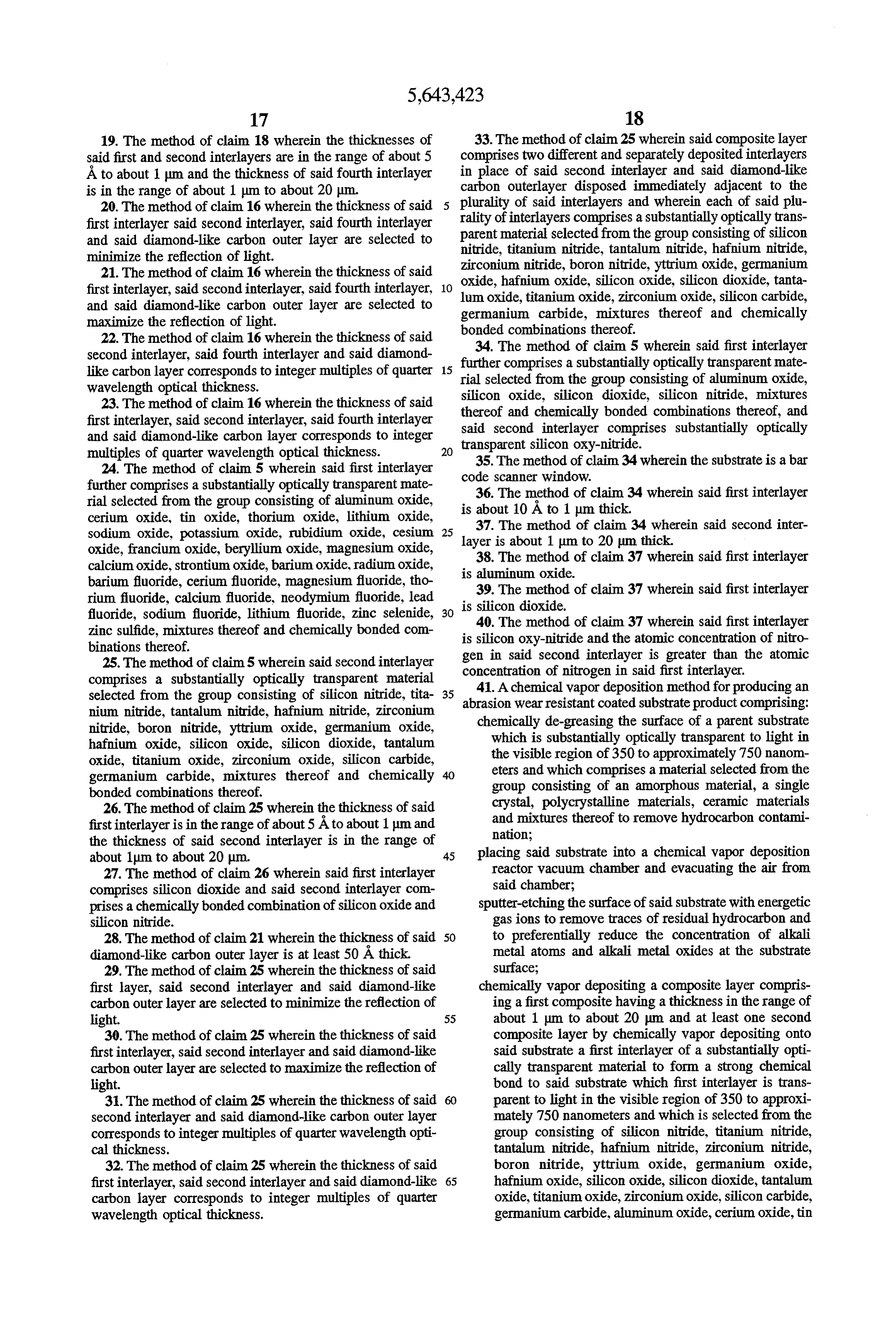
19. The method of claim 18 wherein the thicknesses of 33. The method of claim 25 wherein said composite layer said first and second interlayers are in the range of about 5 comprises two different and separately deposited interlayers A to about 1 m and the thickness of said fourth interlayer in place of said second interlayer and said diamond-like is in the range of about 1 pm to about 20 pm. carbon outerlayer disposed immediately adjacent to the 20. The method of claim 16 wherein the thickness of said plurality of said interlayers and wherein each of said plu first interlayer said second interlayer, said fourth interlayer rality of interlayers comprises a substantially optically trans and said diamond-like carbon outer layer are selected to parent material selected from the group consisting of silicon minimize the reflection of light. nitride, titanium nitride, tantalum nitride, hafnium nitride, 21. The method of claim 16 wherein the thickness of said zirconium nitride, boron nitride, yttrium oxide, germanium first interlayer, said second interlayer, said fourth interlayer, 10 oxide, hafnium oxide, silicon oxide, silicon dioxide, tanta and said diamond-like carbon outer layer are selected to germaniumtitanium lum oxide, oxide, Zirconium oxide, Silicon carbide, carbide, mixtures thereof and chemically maximize the reflection of light. bonded combinations thereof.
22. The method of claim 16 wherein the thickness of said second interlayer, said fourth interlayer and said diamond further 34. The method of claim 5 wherein said first interlayer comprises a substantially optically transparent mate like carbon layer corresponds to integer multiples of quarter 15 rial selected wavelength optical thickness. from the group consisting of aluminum oxide, 23. The method of claim 16 wherein the thickness of said silicon oxide, silicon dioxide, silicon nitride, mixtures first interlayer, said second interlayer, said fourth interlayer said second interlayer bonded thereof and chemically combinations thereof, and comprises substantially optically and said diamond-like carbon layer corresponds to integer transparent silicon oxy-nitride.
multiples of quarter wavelength optical thickness. 20 35. The method of claim 34 wherein the substrate is a bar 24. The method of claim 5 wherein said first interlayer code scanner window.
further comprises a substantially optically transparent mate 36. The method of claim 34 wherein said first interlayer rial selected from the group consisting of aluminum oxide, is about 10 A to 1 um thick.
cerium oxide, tin oxide, thorium oxide, lithium oxide, 37. The method of claim 34 wherein said second inter Sodium oxide, potassium oxide, rubidium oxide, cesium 25 layer is about 1 pm to 20 m thick. oxide, francium oxide, beryllium oxide, magnesium oxide, 38. The method of claim 37 wherein said first interlayer calcium oxide, strontium oxide, barium oxide, radium oxide, is aluminum oxide.
barium fluoride, cerium fluoride, magnesium fluoride, tho rium fluoride, calcium fluoride, neodymium fluoride, lead is silicon dioxide. of claim 37 wherein said first interlayer 39. The method fluoride, sodium fluoride, lithium fluoride, zinc selenide, 30 40. The method of claim 37 wherein said first interlayer zinc sulfide, mixtures thereof and chemically bonded com is silicon oxy-nitride and the atomic concentration of nitro binations thereof.
gen in said second interlayer is greater than the atomic 25. The method of claim.5 wherein said second interlayer concentration comprises a substantially optically transparent material of nitrogen in said first interlayer. 41. A chemical selected from the group consisting of silicon nitride, tita abrasion wear resistant 35 vapor deposition method for producing an nium nitride, tantalum nitride, hafnium nitride, zirconium coated substrate product comprising: nitride, boron nitride, yttrium oxide, germanium oxide, chemically de-greasing the surface of a parent substrate hafnium oxide, silicon oxide, silicon dioxide, tantalum which is substantially optically transparent to light in oxide, titanium oxide, zirconium oxide, silicon carbide, the visible region of 350 to approximately 750 nanom germanium carbide, mixtures thereof and chemically eters and which comprises amaterial selected from the bonded combinations thereof. group consisting of an amorphous material, a single 26. The method of claim 25 wherein the thickness of said crystal, polycrystalline materials, ceramic materials first interlayer is in the range of about 5A to about 1pm and and mixtures thereof to remove hydrocarbon contami the thickness of said second interlayer is in the range of nation;
about 1pm to about 20 um. 45 placing said substrate into a chemical vapor deposition 27. The method of claim 26 wherein said first interlayer reactor vacuum chamber and evacuating the air from comprises silicon dioxide and said second interlayer com said chamber;
prises a chemically bonded combination of silicon oxide and sputter-etching the surface of said substrate with energetic silicon nitride. gas ions to remove traces of residual hydrocarbon and 28. The method of claim 21 wherein the thickness of said 50 to preferentially reduce the concentration of alkali diamond-like carbon outer layer is at least 50 A thick. metal atoms and alkali metal oxides at the substrate 29. The method of claim 25 wherein the thickness of said Surface;
first layer, said second interlayer and said diamond-like chemically vapor depositing a composite layer compris carbon outer layer are selected to minimize the reflection of ing a first composite having a thickness in the range of light. 55 about 1 pm to about 20 m and at least one second 30. The method of claim 25 wherein the thickness of said composite layer by chemically vapor depositing onto first interlayer, said second interlayer and said diamond-like said substrate a first interlayer of a substantially opti carbon outer layer are selected to maximize the reflection of cally transparent material to form a strong chemical light. bond to said substrate which first interlayer is trans 31. The method of claim 25 wherein the thickness of said parent to light in the visible region of 350 to approxi second interlayer and said diamond-like carbon outer layer mately 750 nanometers and which is selected from the corresponds to integer multiples of quarter wavelength opti group consisting of silicon nitride, titanium nitride, cal thickness. tantalum nitride, hafnium nitride, zirconium nitride, 32. The method of claim 25 wherein the thickness of said boron nitride, yttrium oxide, germanium oxide, first interlayer, said second interlayer and said diamond-like 65 hafnium oxide, silicon oxide, silicon dioxide, tantalum carbon layer corresponds to integer multiples of quarter oxide, titanium oxide, zirconium oxide, silicon carbide, wavelength optical thickness. germanium carbide, aluminum oxide, cerium oxide, tin
Page 14
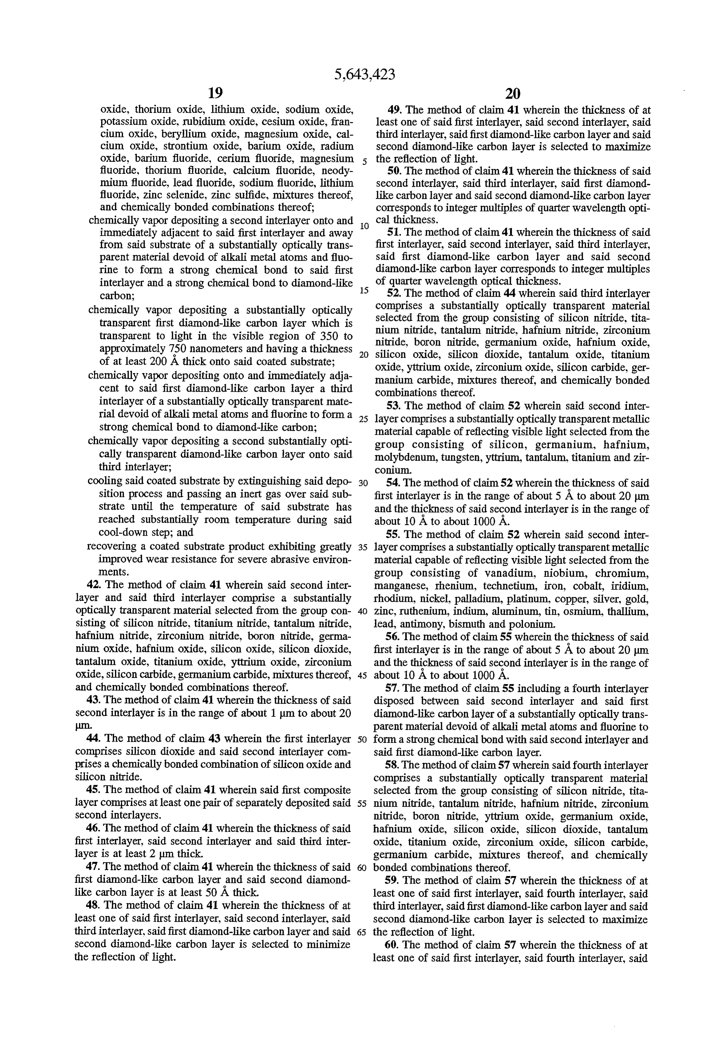
oxide, thorium oxide, lithium oxide, Sodium oxide, 49. The method of claim 41 wherein the thickness of at potassium oxide, rubidium oxide, cesium oxide, fran least one of said first interlayer, said second interlayer, said cium oxide, beryllium oxide, magnesium oxide, cal third interlayer, said first diamond-like carbon layer and said cium oxide, strontium oxide, barium oxide, radium second diamond-like carbon layer is selected to maximize oxide, barium fluoride, cerium fluoride, magnesium 5 the reflection of light.
fluoride, thorium fluoride, calcium fluoride, neody 50. The method of claim 41 wherein the thickness of said mium fluoride, lead fluoride, sodium fluoride, lithium second interlayer, said third interlayer, said first diamond fluoride, zinc selenide, zinc sulfide, mixtures thereof, like carbon layer and said second diamond-like carbon layer and chemically bonded combinations thereof; corresponds to integer multiples of quarter wavelength opti chemically vapor depositing a second interlayer onto and O cal thickness.
immediately adjacent to said first interlayer and away 51. The method of claim 41 wherein the thickness of said from said substrate of a substantially optically trans first interlayer, said second interlayer, said third interlayer, parent material devoid of alkali metal atoms and fluo said first diamond-like carbon layer and said second rine to form a strong chemical bond to said first diamond-like carbon layer corresponds to integer multiples interlayer and a strong chemical bond to diamond-like 15 of quarter wavelength optical thickness. carbon; 52. The method of claim 44 wherein said third interlayer chemically vapor depositing a substantially optically comprises a substantially optically transparent material transparent first diamond-like carbon layer which is selected from the group consisting of silicon nitride, tita nium nitride, tantalum nitride, hafnium nitride, Zirconium transparent to light in the visible region of 350 to nitride, boron nitride, germanium oxide, hafnium oxide, approximately 750 nanometers and having a thickness 20 silicon oxide, silicon dioxide, tantalum oxide, titanium of at least 200 A thick onto said coated substrate; oxide, yttrium oxide, zirconium oxide, silicon carbide, ger chemically vapor depositing onto and immediately adja manium carbide, mixtures thereof, and chemically bonded cent to said first diamond-like carbon layer a third combinations thereof.
interlayer of a substantially optically transparent mate 53. The method of claim 52 wherein said second inter rial devoid of alkali metal atoms and fluorine to form a 25 layer comprises a substantially optically transparent metallic strong chemical bond to diamond-like carbon; material capable of reflecting visible light selected from the chemically vapor depositing a second substantially opti group consisting of silicon, germanium, hafnium, cally transparent diamond-like carbon layer onto said molybdenum, tungsten, yttrium, tantalum, titanium and Zir third interlayer; conium.
cooling said coated Substrate by extinguishing said depo 30 54. The method of claim 52 wherein the thickness of said sition process and passing an inert gas over said sub first interlayer is in the range of about 5 A to about 20 pm strate until the temperature of said substrate has and the thickness of said second interlayer is in the range of reached substantially room temperature during said about 10A to about 1000 A.
cool-down step; and 55. The method of claim 52 wherein said second inter recovering a coated substrate product exhibiting greatly 35 layer comprises a substantially optically transparent metallic improved wear resistance for severe abrasive environ material capable of reflecting visible light selected from the mentS. group consisting of vanadium, niobium, chromium, 42. The method of claim 41 wherein said second inter manganese, rhenium, technetium, iron, cobalt, iridium, layer and said third interlayer comprise a substantially rhodium, nickel, palladium, platinum, copper, silver, gold, optically transparent material selected from the group con 40 Zinc, ruthenium, indium, aluminum, tin, osmium, thallium, sisting of silicon nitride, titanium nitride, tantalum nitride, lead, antimony, bismuth and polonium. hafnium nitride, zirconium nitride, boron nitride, germa 56. The method of claim 55 wherein the thickness of said nium oxide, hafnium oxide, silicon oxide, silicon dioxide, first interlayer is in the range of about 5 A to about 20 pm tantalum oxide, titanium oxide, yttrium oxide, zirconium and the thickness of said second interlayer is in the range of oxide, silicon carbide, germanium carbide, mixtures thereof, 45 about 10 A to about 1000 A.
and chemically bonded combinations thereof. 57. The method of claim 55 including a fourth interlayer 43. The method of claim 41 wherein the thickness of said disposed between said second interlayer and said first second interlayer is in the range of about 1 um to about 20 diamond-like carbon layer of a substantially optically trans Im. parent material devoid of alkali metal atoms and fluorine to 44. The method of claim 43 wherein the first interlayer 50 form a strong chemical bond with said second interlayer and comprises silicon dioxide and said second interlayer com said first diamond-like carbon layer.
prises a chemically bonded combination of silicon oxide and 58. The method of claim 57 wherein said fourth interlayer silicon nitride. comprises a substantially optically transparent material 45. The method of claim 41 wherein said first composite selected from the group consisting of silicon nitride, tita layer comprises at least one pair of separately deposited said nium nitride, tantalum nitride, hafnium nitride, Zirconium second interlayers. nitride, boron nitride, yttrium oxide, germanium oxide, 46. The method of claim 41 wherein the thickness of said hafnium oxide, silicon oxide, silicon dioxide, tantalum first interlayer, said second interlayer and said third inter oxide, titanium oxide, zirconium oxide, silicon carbide, layer is at least 2 um thick. germanium carbide, mixtures thereof, and chemically 47. The method of claim 41 wherein the thickness of said bonded combinations thereof.
first diamond-like carbon layer and said second diamond 59. The method of claim 57 wherein the thickness of at like carbon layer is at least 50 A thick. least one of said first interlayer, said fourth interlayer, said 48. The method of claim 41 wherein the thickness of at third interlayer, said first diamond-like carbon layer and said least one of said first interlayer, said second interlayer, said second diamond-like carbon layer is selected to maximize third interlayer, said first diamond-like carbon layer and said 65 the reflection of light.
second diamond-like carbon layer is selected to minimize 60. The method of claim 57 wherein the thickness of at the reflection of light. least one of said first interlayer, said fourth interlayer, said
Page 15
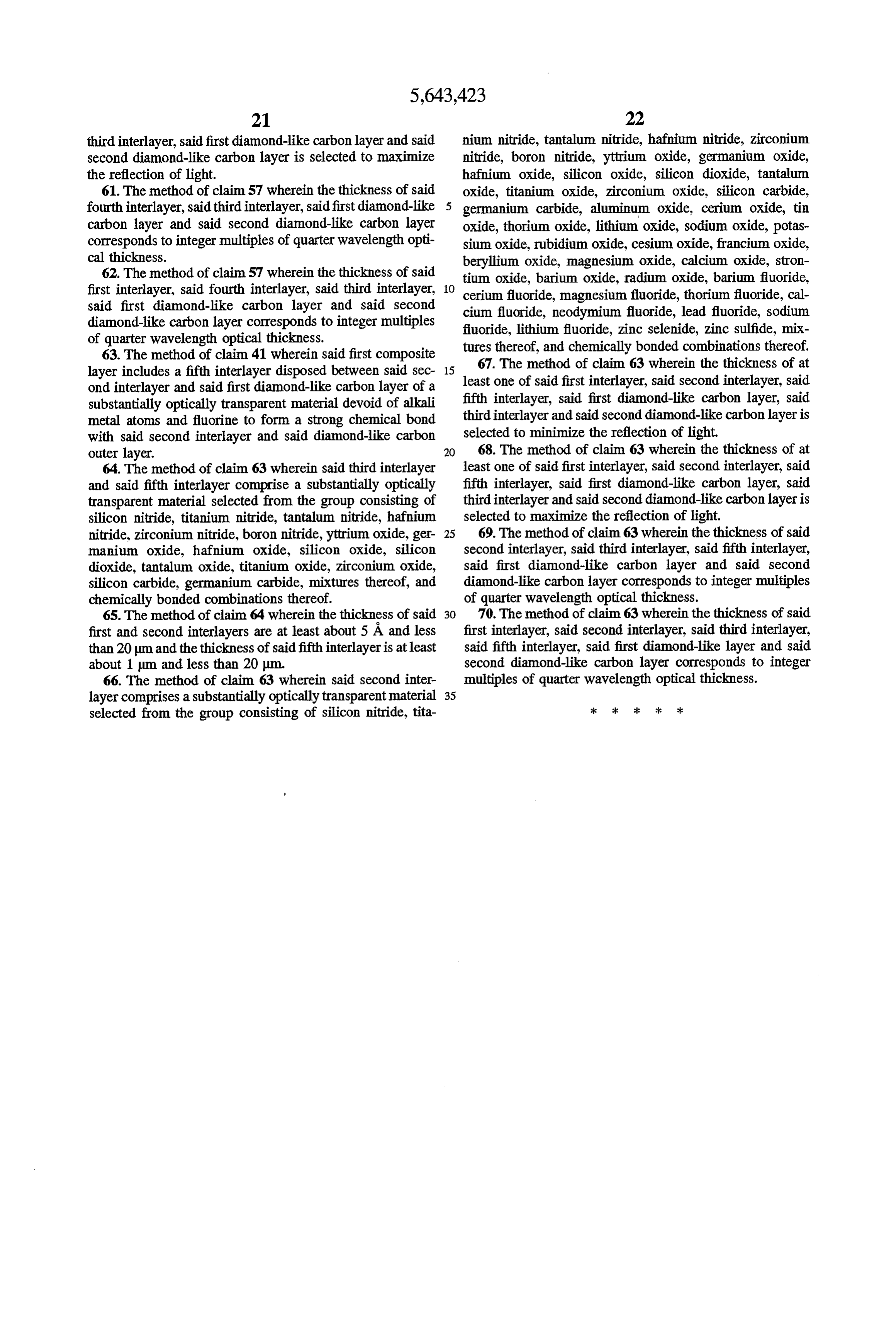
third interlayer, said first diamond-like carbon layer and said nium nitride, tantalum nitride, hafnium nitride, zirconium second diamond-like carbon layer is selected to maximize nitride, boron nitride, yttrium oxide, germanium oxide, the reflection of light. hafnium oxide, silicon oxide, silicon dioxide, tantalum 61. The method of claim 57 wherein the thickness of said oxide, titanium oxide, zirconium oxide, silicon carbide, fourth interlayer, said third interlayer, said first diamond-like germanium carbide, aluminum oxide, cerium oxide, tin carbon layer and said second diamond-like carbon layer oxide, thorium oxide, lithium oxide, sodium oxide, potas corresponds to integer multiples of quarter wavelength opti sium oxide, rubidium oxide, cesium oxide, francium oxide, cal thickness. beryllium oxide, magnesium oxide, calcium oxide, stron 62. The method of claim 57 wherein the thickness of said first interlayer, said fourth interlayer, said third interlayer, 10 tium cerium oxide, barium oxide, radium oxide, barium fluoride, fluoride, magnesium fluoride, thorium fluoride, cal said first diamond-like carbon layer and said second cium fluoride, neodymium fluoride, lead fluoride, sodium diamond-like carbon layer corresponds to integer multiples fuoride, lithium fluoride, zinc selenide, zinc sulfide, mix of quarter wavelength optical thickness.
63. The method of claim 41 wherein said first composite tures 67.
thereof, and chemically bonded combinations thereof.
The method of claim 63 wherein the thickness of at layer includes a fifth interlayer disposed between said sec 15 ond interlayer and said first diamond-like carbon layer of a least one of said first interlayer, said second interlayer, said Substantially optically transparent material devoid of alkali fifth interlayer, said first diamond-like carbon layer, said metal atoms and fluorine to form a strong chemical bond third interlayer and said second diamond-like carbon layeris with said second interlayer and said diamond-like carbon selected to minimize the reflection of light. outer layer. 20 68. The method of claim 63 wherein the thickness of at 64. The method of claim 63 wherein said third interlayer least one of said first interlayer, said second interlayer, said and said fifth interlayer comprise a substantially optically fifth interlayer, said first diamond-like carbon layer, said transparent material selected from the group consisting of third interlayer and said second diamond-like carbon layer is silicon nitride, titanium nitride, tantalum nitride, hafnium selected to maximize the reflection of light. nitride, zirconium nitride, boron nitride, yttrium oxide, ger 25 69. The method of claim 63 wherein the thickness of said manium oxide, hafnium oxide, silicon oxide, silicon second interlayer, said third interlayer, said fifth interlayer, dioxide, tantalum oxide, titanium oxide, zirconium oxide, said first diamond-like carbon layer and said second silicon carbide, germanium carbide, mixtures thereof, and diamond-like carbon layer corresponds to integer multiples chemically bonded combinations thereof. of quarter wavelength optical thickness. 65. The method of claim 64 wherein the thickness of said 30 70. The method of claim 63 wherein the thickness of said first and second interlayers are at least about 5 A and less first interlayer, said second interlayer, said third interlayer, than 20 m and the thickness of said fifth interlayer is at least said fifth interlayer, said first diamond-like layer and said about 1 m and less than 20 p.m. second diamond-like carbon layer corresponds to integer 66. The method of claim 63 wherein said second inter multiples of quarter wavelength optical thickness. layer comprises a substantially optically transparent material 35 selected from the group consisting of silicon nitride, tita :: * : *k sk
Page 16
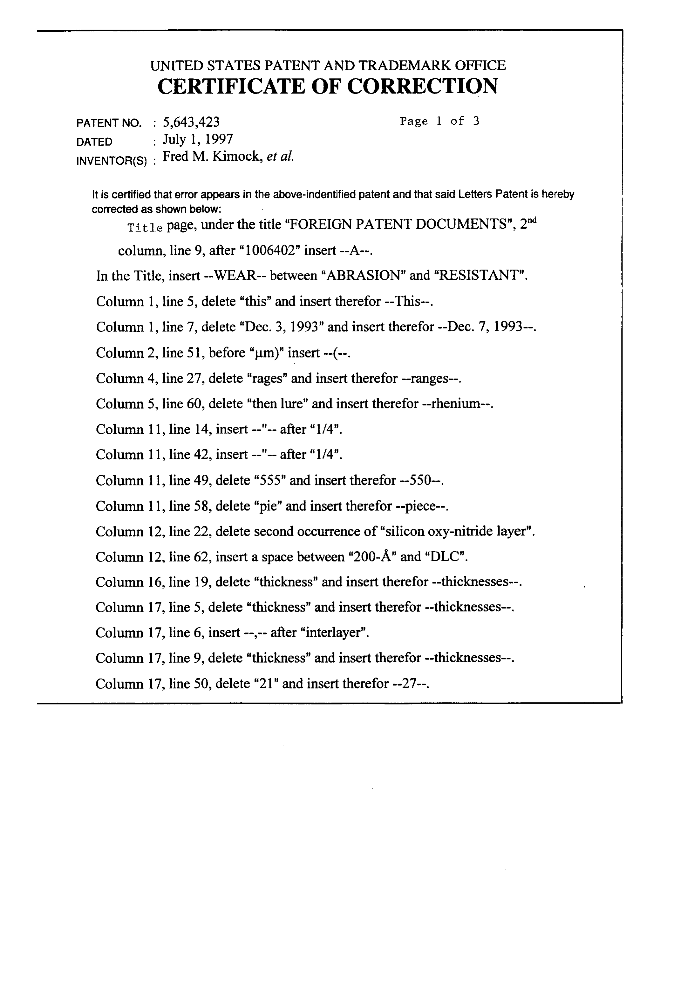
UNITED STATES PATENT AND TRADEMARK OFFICE
CERTIFICATE OF CORRECTION
PATENT NO. : 5,643,423 Page 1 of 3
INVENTOR(s): Fred M. Kimock, et al.
it is certified that error appears in the above-indentified patent and that said Letters Patent is hereby Corrected as shown below:
Title page, under the title "FOREIGN PATENT DOCUMENTS", 2" column, line 9, after "1006402" insert --A-.
In the Title, insert-WEAR-- between "ABRASION" and "RESISTANT". Column 1, line 5, delete "this" and insert therefor--This--. Column 1, line 7, delete "Dec. 3, 1993" and insert therefor-Dec. 7, 1993--. Column 2, line 51, before "um)" insert -(--.
Column 4, line 27, delete "rages" and insert therefor-ranges--. Column 5, line 60, delete "then lure" and insert therefor--rhenium--.
Column 11, line 49, delete "555" and insert therefor-550-. Column 11, line 58, delete "pie" and insert therefor-piece--. Column 12, line 22, delete second occurrence of "silicon oxy-nitride layer". Column 12, line 62, insert a space between "200-A" and "DLC". Column 16, line 19, delete "thickness" and insert therefor--thicknesses--. Column 17, line 5, delete "thickness" and insert therefor--thicknesses--. Column 17, line 6, insert ---- after "interlayer".
Column 17, line 9, delete "thickness" and insert therefor--thicknesses--. Column 17, line 50, delete "21" and insert therefor-27--.
Page 17
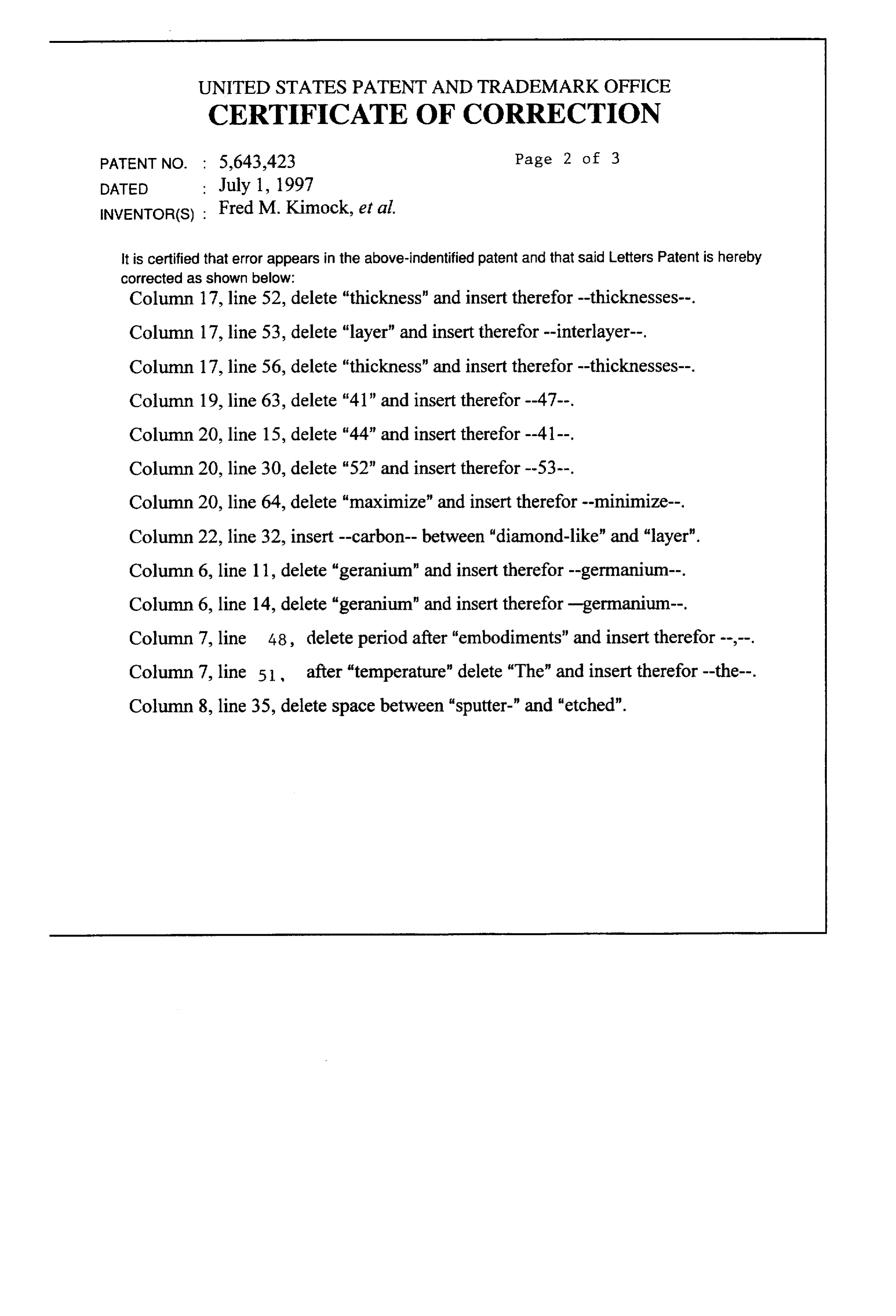
UNITED STATES PATENT AND TRADEMARK OFFICE
CERTIFICATE OF CORRECTION
PATENT NO. : 5,643,423 Page 2 of 3
INVENTOR(s): Fred M. Kimock, et al.
It is certified that error appears in the above-indentified patent and that said Letters Patent is hereby Corrected as shown below:
Column 17, line 52, delete "thickness" and insert therefor--thicknesses--. Column 17, line 53, delete "layer" and insert therefor-interlayer--. Column 17, line 56, delete "thickness" and insert therefor--thicknesses--. Column 19, line 63, delete "41" and insert therefor-47--.
Column 20, line 15, delete "44" and insert therefor-41 --.
Column 20, line 30, delete "52" and insert therefor-53--.
Column 20, line 64, delete "maximize" and insert therefor-minimize--. Column 22, line 32, insert -carbon-between "diamond-like" and "layer". Column 6, line 11, delete "geranium" and insert therefor-germanium--. Column 6, line 14, delete "geranium" and insert therefor-germanium--. Column 7, line 48, delete period after "embodiments" and insert therefor ----. Column 7, line 51, after "temperature" delete "The" and insert therefor--the--. Column 8, line 35, delete space between "sputter-" and "etched".
Page 18
UNITED STATES PATENT AND TRADEMARK OFFICE
CERTIFICATE OF CORRECTION
DATED July 1, 1997 Page 3 of 3 INVENTOR(s): Fred M. Kimock, et al.
It is certified that error appears in the above-indentified patent and that said Letters Patent is hereby Corrected as shown below:
Column 10, line 37, delete "." after "silicate" and before")". Column 12, line 40, insert --A-- before "5.7".
Column 13, line 4, insert --was-- before "deposited".
Column 15, line 43, delete "and capable of forming" and insert therefor--to form--.
Signed and Sealed this
Twenty-sixth Day of May, 1998
BRUCE LEHMAN
Attesting Officer Commissioner of Patents and Trademarks
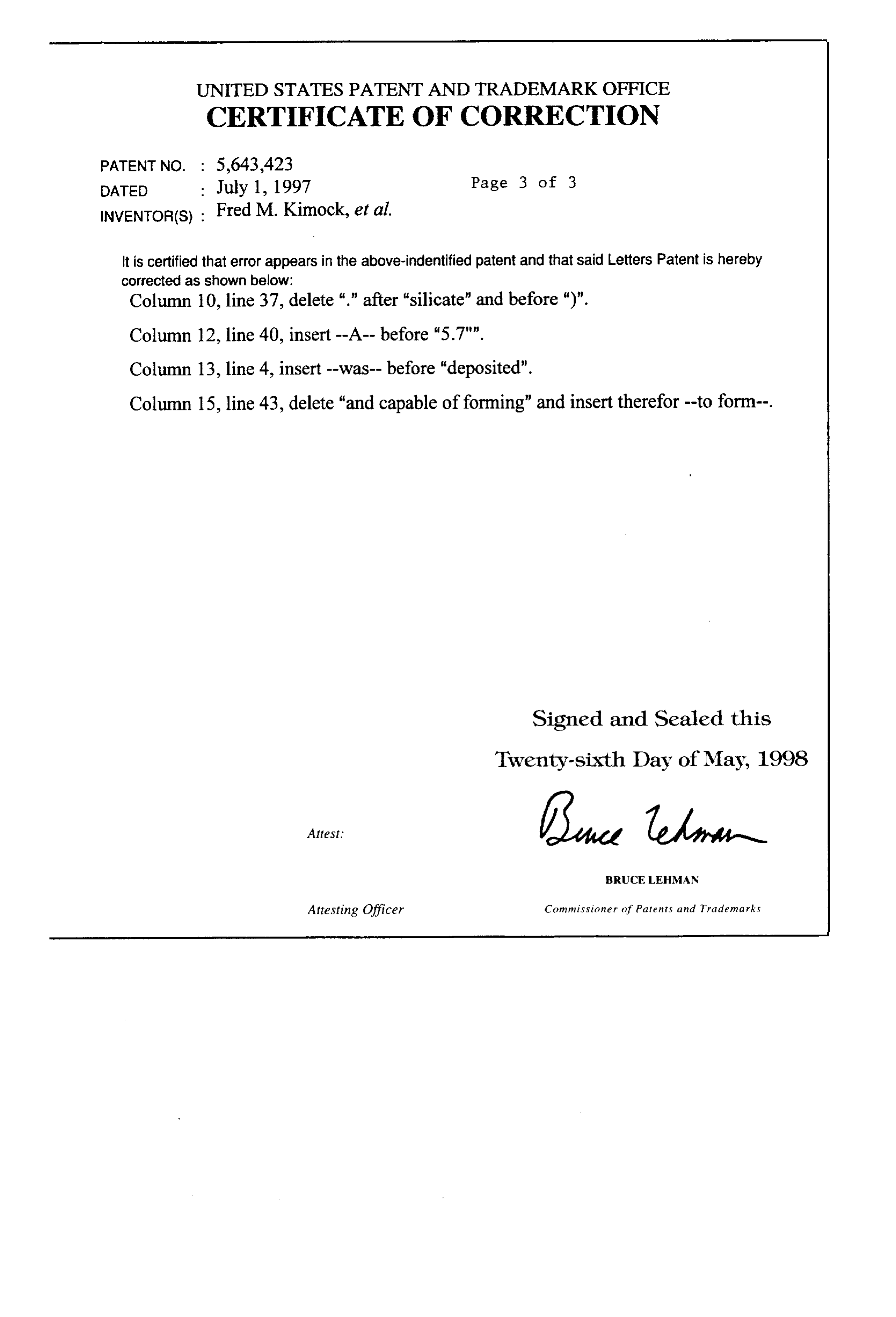
Provenance
- Collection
- Cited prior art
- Original PDF
- patentimages.storage.googleapis.com →
- Filed
- 1993-12-03
- Pages
- 18
- Method
- pdftotext (the PDF's own text layer) + pdftoppm 300dpi page scans
- Source
- Google Patents bibliographic record
- Granted
- 1997-07-01
- Inventors
- Fred M. Kimock; Bradley J. Knapp; Steven James Finke; Monsanto Co
- Transcribed from
- patentimages.storage.googleapis.com →