patent · US5525466
Multiple output referencing system for evanescent wave sensor
11 June 1996
Page 1 — bibliographic record
United States Patent (19) 11 Patent Number: 5,525,466 Slovacek et al. 45) Date of Patent: *Jun. 11, 1996 (54) MULTIPLE OUTPUT REFERENCING 4,775,637 - 10/1988 Sutherland et al. .................... 436/527 SYSTEM FOR EVANESCENT WAVE SENSOR 5,156,976. 10/1992 Slovacek et al. ......... ... 436/164 5,340,715 8/1994 Slovacek et al. ........................... 435/6
(T5) Inventors: Rudolf E. Slovacek, Norfolk, Mass.;
Walter F. Love, Horseheads, N.Y., OTHER PUBLICATIONS
Richard L. Schulkind, Sharon; Irene Stewart, G. et al. Referencing Systems for Evanescent Wave M. Walczak, Boston, both of Mass.; Sensors. Proc. of SPIE (1990) 1314; 262-269.
Thomas A. Cook, Corning, N.Y. Bluestein, B.I. et al. Fiber Optic Evanescent Wave Immu 73) Assignee: Ciba Corning Diagnostics Corp., nosensors for Medical Diagnostics. Trends Biotechnol. (Jun. Medfield, Mass. 1990) 8:161-168.
Sutherland, R. M. et al. Immunoassays at a Quartz-Liquid
Notice: The term of this patent shall not extend Interface:Theory Instrumentation and . . . . . J. Immuno. beyond the expiration date of Pat. No. Methods (1984) 74:253-265.
Primary Examiner-James C. Housel 21 Appl. No.: 246,391 Assistant Examiner-Christopher L. Chin Attorney, Agent, or Firm-Arthur S. Morgenstern; Judith A.
22 Filed: May 20, 1994 Roesler
Related U.S. Application Data 57 ABSTRACT (63 Continuation of Ser. No. 712,304, Jun. 7, 1991, abandoned. An evanescent wave system and method including an optical (51) Int. Cl. ......................... G01N 33/552; G01N 3/68 sensor for use in assaying a reference material and at least 52 U.S. Cl. .............................. 435/6; 356/243; 356/306; one molecular species or analyte in a test medium or test sample for diagnostic and other applicable purposes. The 356/448; 385/12;385/129; 385/130; 422/82.05; sensor includes a waveguide for propagating a radiation 422/82.08; 422/82.11; 435/287.2, 435/287.9; input along its length. The radiation input causes evanescent 435/808; 435/288.7; 436/164; 436/172; electromagnetic waves that are capable of stimulating output 436/527; 436/805 emissions that are indicative of a reference material and of 58) Field of Search ............................ 385/12, 129, 130; one or more molecular species or analytes. By comparing 356/243, 306, 448; 422/82.05, 82.08, 82.11; the emission(s) indicative of the reference material to the 435/6, 287, 291, 808; 436/518, 527, 164, emission indicative of the presence of the molecular species 172,805 or analyte, the presence and concentration of the molecule in
the sample can be determined. The reference material pro vides for normalization and/or calibration of the system.
4,558,04 12/1985 Hirschfeld et al. ..................... 436/527 17 Claims, 9 Drawing Sheets
Page 2
Drawing sheet — no readable text.
Page 3
Drawing sheet — no readable text.
Page 4
Drawing sheet — no readable text.
Page 5
Drawing sheet — no readable text.
Page 6
Drawing sheet — no readable text.
Page 7
Drawing sheet — no readable text.
Page 8
Drawing sheet — no readable text.
Page 9
Drawing sheet — no readable text.
Page 10
Drawing sheet — no readable text.
Page 11
MULTIPLE OUTPUT REFERENCING core material. A reactant coating is disposed about the SYSTEM FOR EVANESCENT WAVE SENSOR opening within the core on a single optical surface. There is, however, a need for providing an evanescent
This is a continuation application of Ser. No. 07/712,304 sensor which can normalize or calibrate for variations in filed on Jun. 7, 1991, now abandoned. signal input and signal collecting efficiencies as well as
FIELD OF THE INVENTION
defects in the optical surface or geometry. For example, a decrease in diameter along the length of a solid rod or of wall
This invention relates to an evanescent wave system thickness of a hollow fiber optic waveguide changes the including an optical processor sensor, for use in assays of 10 angle of light input at which light is totally internally one or more analytes or molecules in a test medium, and a reflected. This may cause the radiation to eventually strike reference material and, more particularly, to such a sensor the waveguide surface at an angle less than the critical angle which generates two or more output signals from one or and therefore escape the waveguide, changing the evanes more wave propagating surface. The reference material cent signal. Alternatively, if the diameter increases along the provides for normalization and/or calibration of the system. 15 length of a rod or wall of the waveguide, the angle of light propagating therethrough may become increasingly greater
TECHNICAL DISCLOSURE than the critical angle, and there will be fewer reflections and a lower propagation angle, both of which reduce the amount
There are a number of optical devices which propagate of evanescent wave electromagnetic field strength which is radiation by "total internal reflection", see Harrick, N.J., delivered to a medium.
Internal Reflection Spectroscopy, Harrick Scientific Corp., 20 Another problem concerns irregularities in the wave Ossining, N.Y. (Third printing 1987), to generate an eva propagating surface of the sensor, altering the amount of nescent wave at the interface of the device and a medium or signal output detected.
test sample having a lower index of refraction. The evanes Accordingly, it is among the objects of the invention to cent wave is an electromagnetic waveform which typically extends less than a wavelength into the test medium. How 25 provide
an improved evanescent wave system where the apparatus includes a sensor, for use in assays of ever, this penetration is sufficient to permit interaction analytes or molecules in a medium or test sample and a between the evanescent wave component and an analyte in reference material, and more particularly, to such a sensor the medium.
which
One example of such devices is the use of waveguides in 30 more wave generates two or more output signals from one or the area of fluorescent immunoassays. Waveguides in the propagating surfaces. The reference material form of fiber optic waveguides are coated with a reactant provides for normalization and/or calibration of the system. A primary object of the invention coating including, for example, either an antibody or an processor for a multifrequency evanescent is to provide an optical antigen, which binds the corresponding antigen or antibody, wave system. respectively, if present, in a medium. This reactant coating 35 Another object of the invention is to provide an evanes is typically attached to the waveguide prior to the perfor cent wave sensor having two or more fluorophores. mance of the assay. In a "sandwich' immunoassay, an Yet another object of the invention is to provide an antibody is coated to the surface of the fiber optic waveguide evanescent wave system including a sensor and a reference to form a reactant coating, and the waveguide is contacted material, the reference material functioning to normalize with a medium believed to contain the antigen (analyte) to 40 and/or calibrate for variations in the sensor and instrument be analyzed, and an added second antibody, previously to sensor coupling efficiency which affect the signal input labelled with a fluorescent molecule. Alternatively, in a and signal collection.
"competitive' assay, a fluorescently labelled antigen is first A still further object of the invention is to provide a sensor mixed with the medium suspected of containing an antigen that allows at least one analyte and a reference material to be and the mixture is brought into contact with the reactant analyzed by a wave propagating surface. coated waveguide. In either technique, the coated antibody 45 Another object of the invention is to provide an evanes binds with the antigen to form a complex attached to the cent wave system which can compensate for variations fiber optic waveguide. between different sensors.
Electromagnetic radiation is introduced into the fiber Yet another object of the invention is to provide an optic waveguide at one or more predetermined sets of 50 evanescent wave system including a sensor that provides wavelength bands and is propagated along the waveguide by accurate output signals that are corrected for changes in "total internal reflection'. The reflection is, of course, not those things which cause signal variations by the sensor. completely total as, for example, a fluorescent molecule Another object of the invention is to provide a sensor absorbs a small amount of evanescent radiation.
The attached fluorescent molecule (referred to as a fluo 55 incorporating a reference material.
rophore) absorbs energy from the evanescent wave at a first SUMMARY OF THE INVENTION set of wavelengths and fluoresces at a second, longer set of wavelengths. Fluorescence from the excited fluorophore In a first embodiment of the invention, analysis of both passes into the optical waveguide via a tunneling effect and one or more analytes and a reference material is achieved by the portion of the fluorescent radiation which passes within 60 attaching a reactant coating and a reference material onto an the waveguide at an angle greater than the critical angle is propagated through the waveguide to emerge as an output same wave sensor evanescent and, in a preferred embodiment, on the propagating surface from which the reference signal. material and analyte(s) are sensed in the evanescent Zone. Several improved waveguides are described by Keck et The reference material functions to normalize and/or cali al., in U.S. Pat. No. 4,880,752 which is incorporated herein 65 brate the system. Alternatively, the reference material may by reference. In one construction, the waveguide has an be physically independent of the sensor and yet still function elongated, rod-shaped core having an opening within the to normalize and/or calibrate the system.
Page 12
In use, the invention allows output signals from both the rial is used as a reference for itself. This embodiment reference material and the analyte to be detected so as to provides the advantage of a reduced signal to noise ratio vs. provide a means for normalizing and calibrating the system a two fluoromer system.
for any variations in the sensor and instrument to sensor Each embodiment of the invention is operable in a system coupling efficiency which affect the signal input and signal including an optical processor. collection. See Harrick, infra, and Love, W. F., Bulton, L.J., and Slovacek, R. E., "Optical Characteristics of Fiber Optic DESCRIPTION OF THE DRAWINGS Evanescent Wave Sensors' printed in Biosensors With
Fiberoptics, D. Wise and L. Wingard, Editors, Humana The foregoing and other objects and advantages of the Press, Clifton, N.J. both of which are incorporated herein by 10 invention will be appreciated more fully from the following reference. Since any geometric variations or surface irregu further description thereof with reference to the accompa larities in the sensor will affect the known output signal from nying drawings wherein:
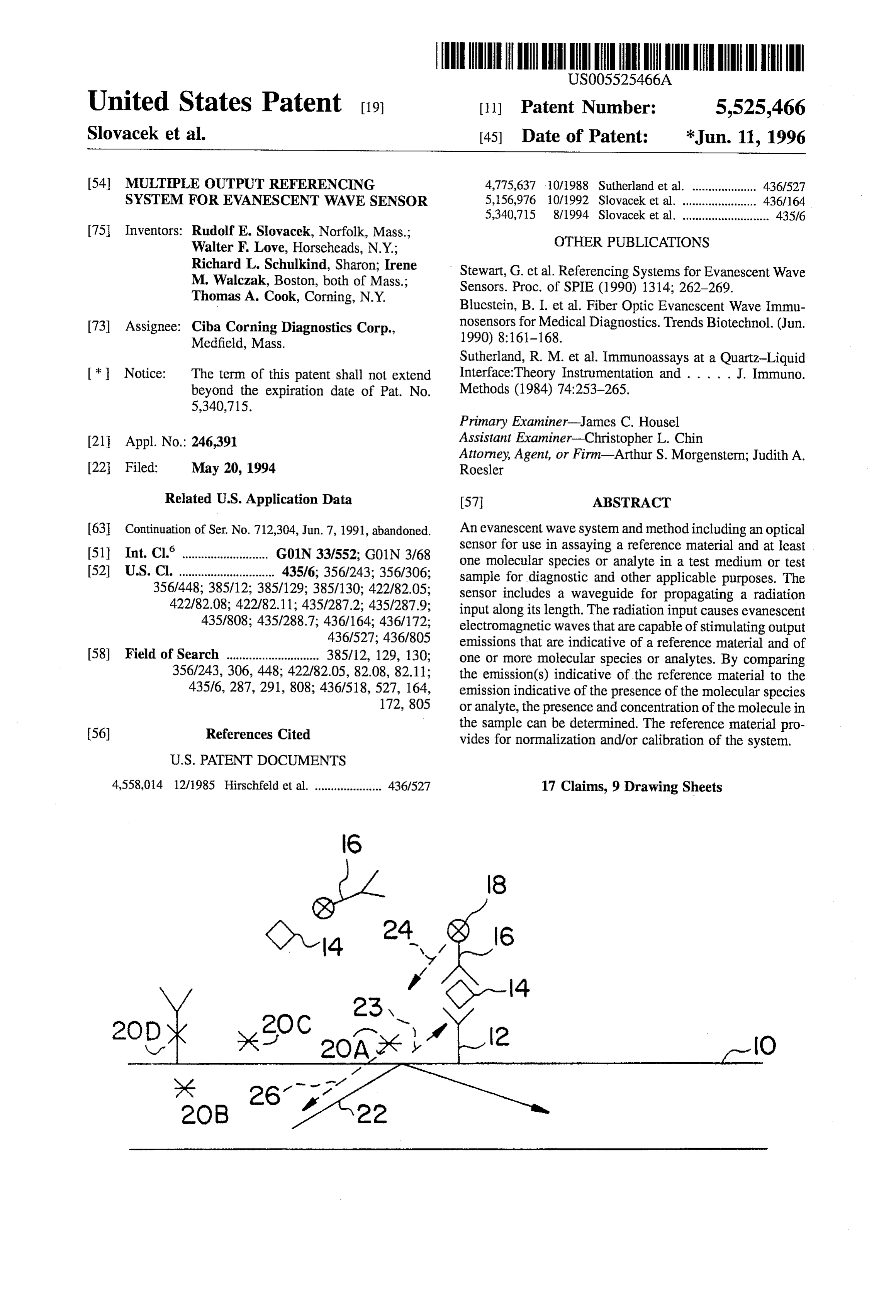
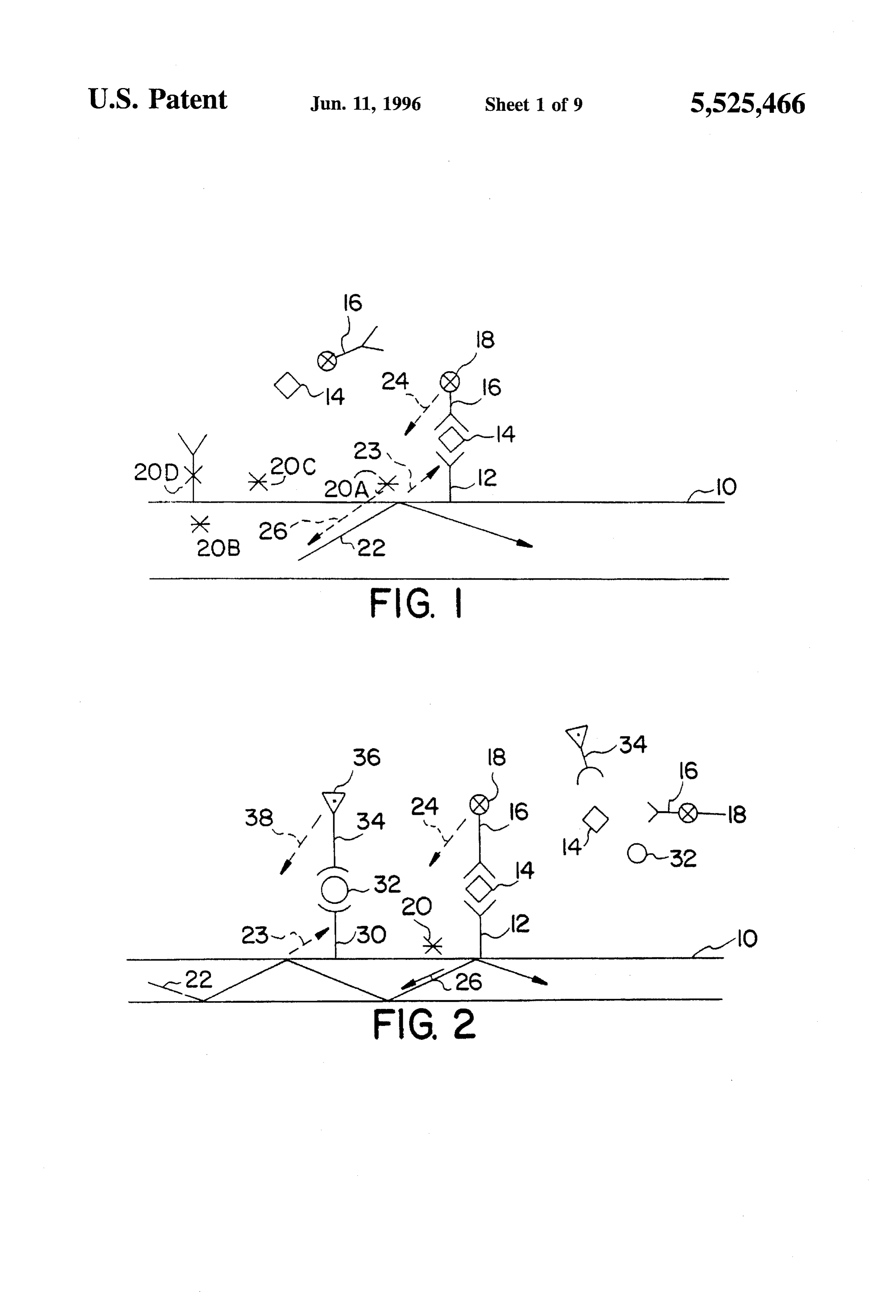
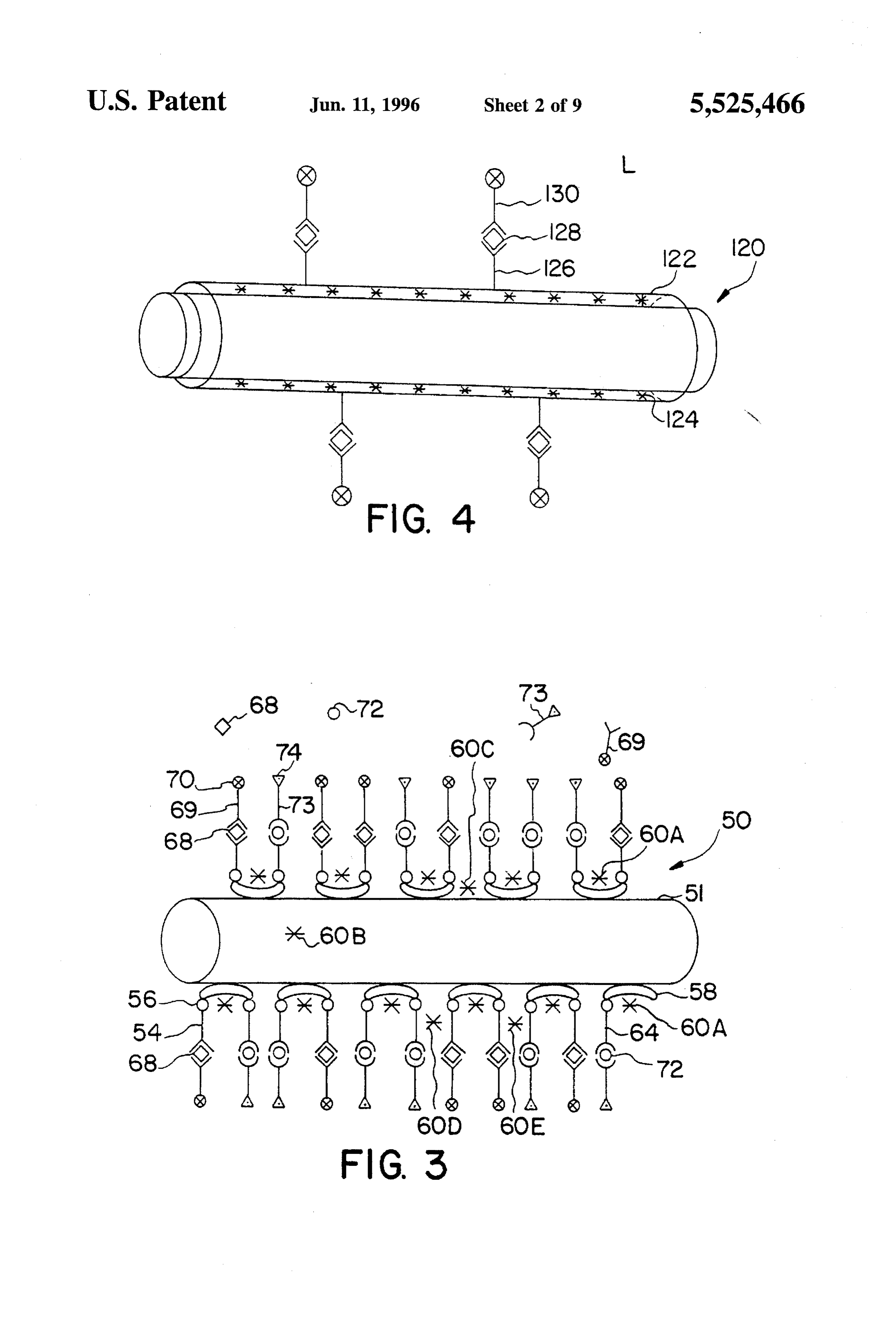
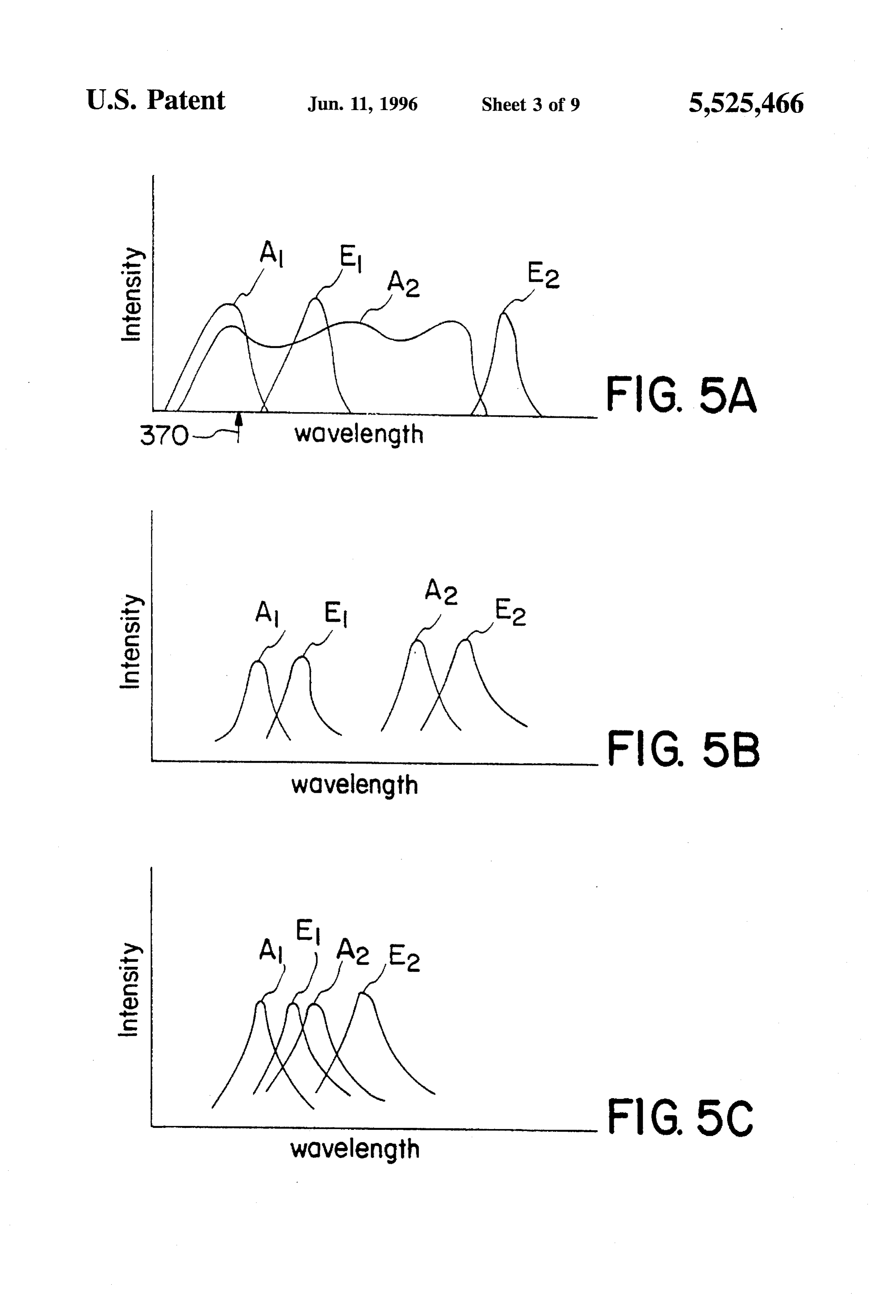
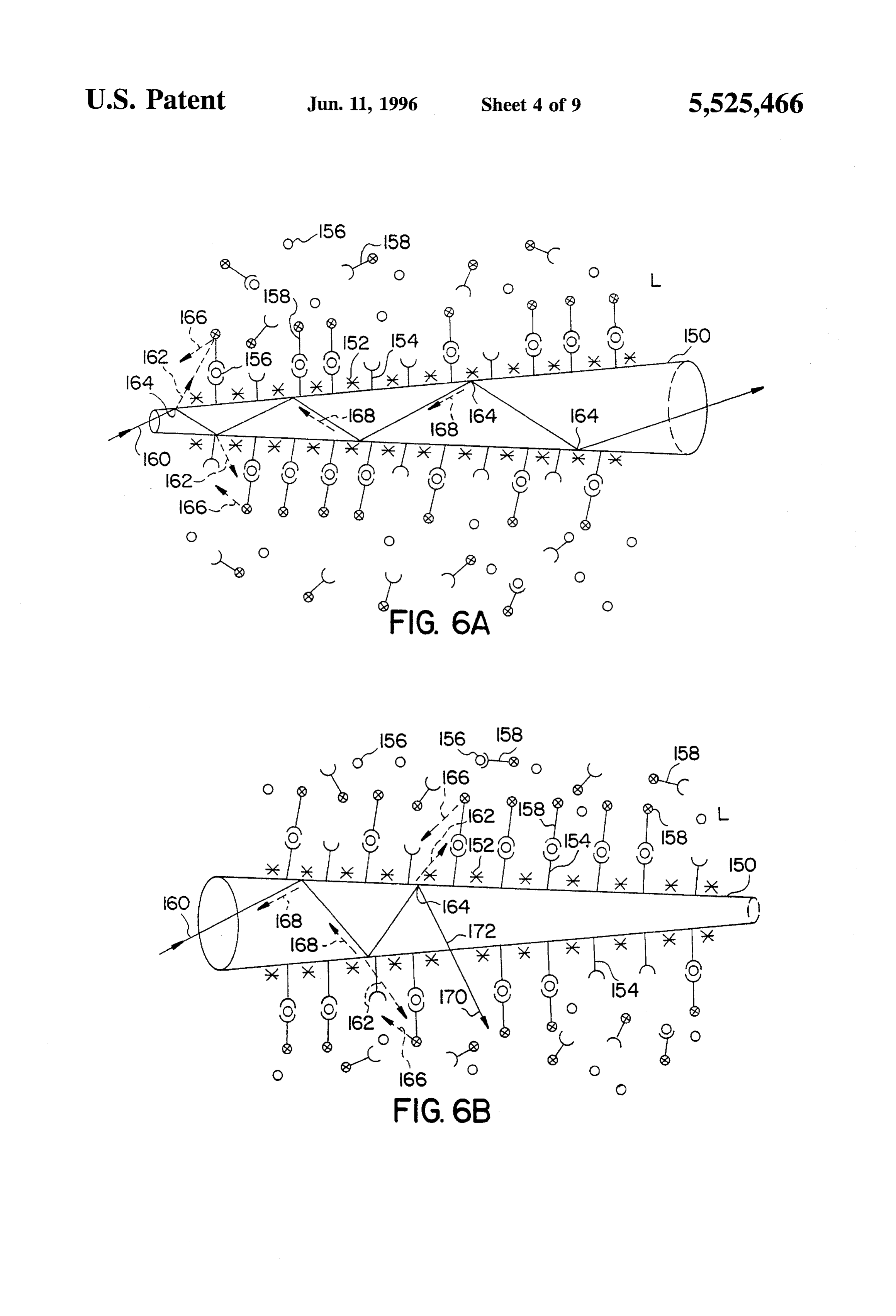
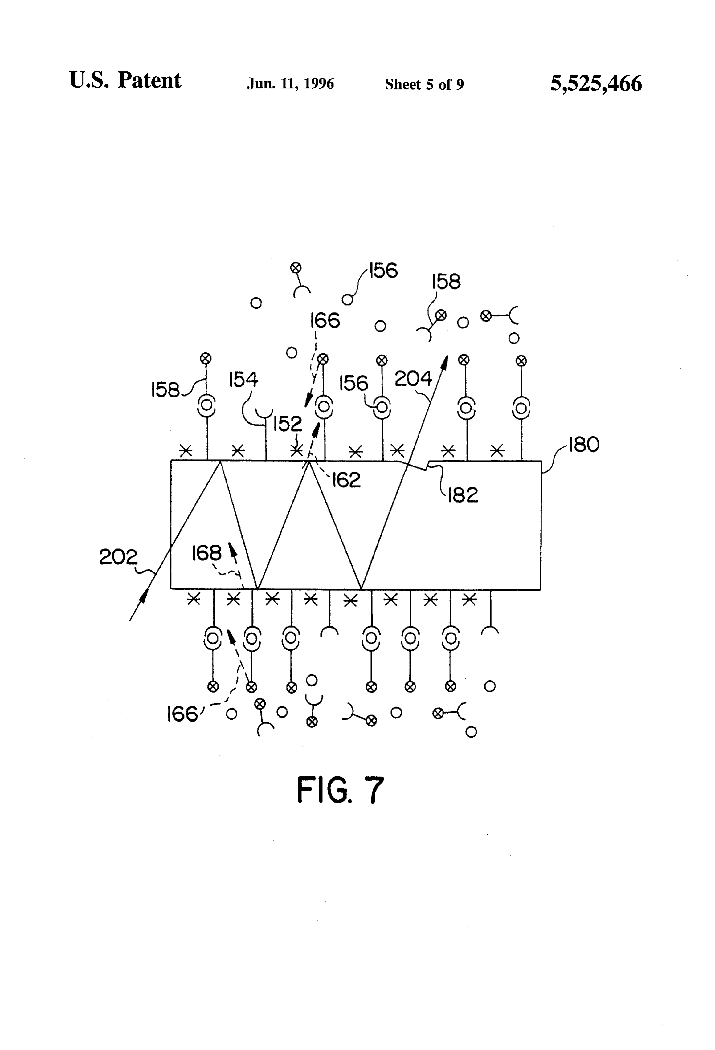
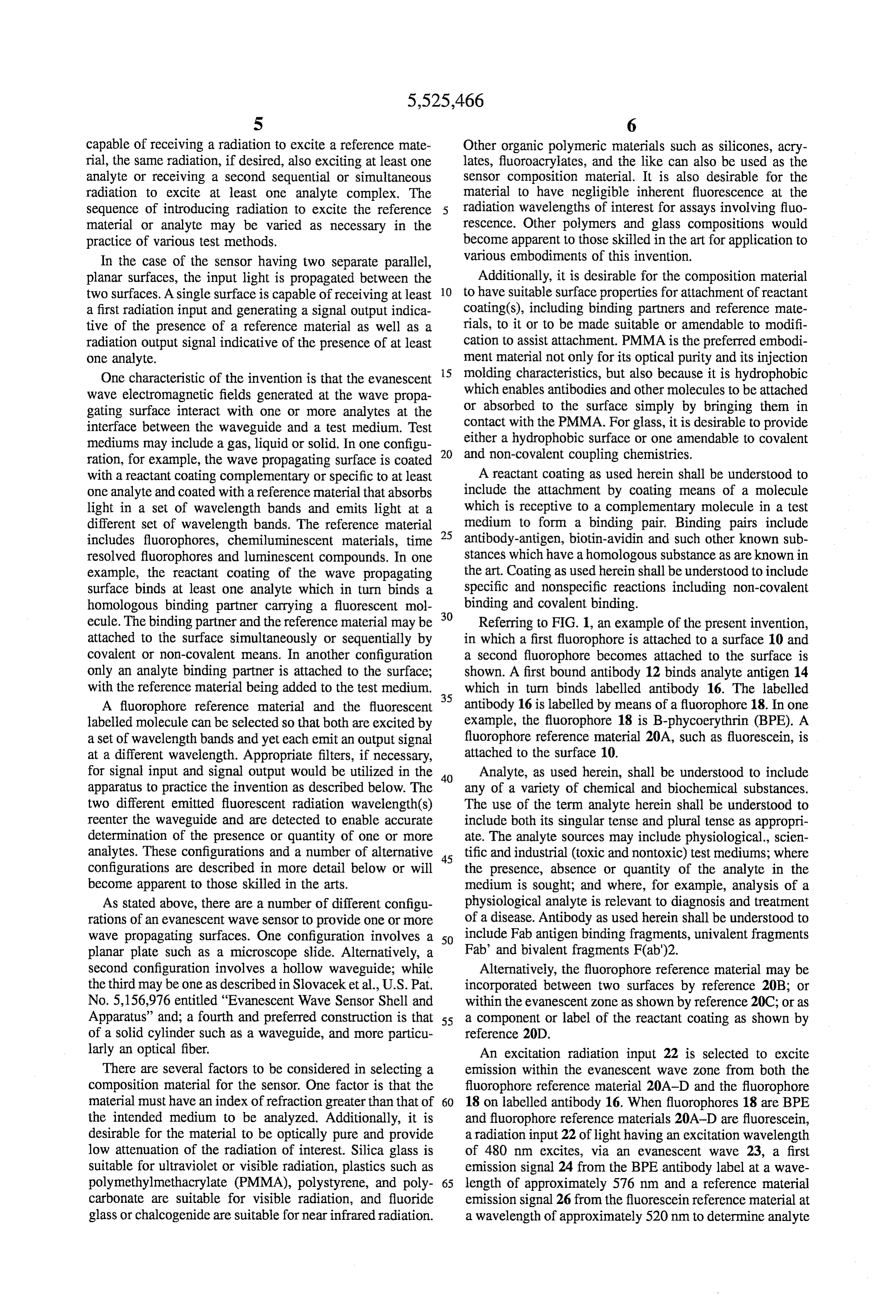
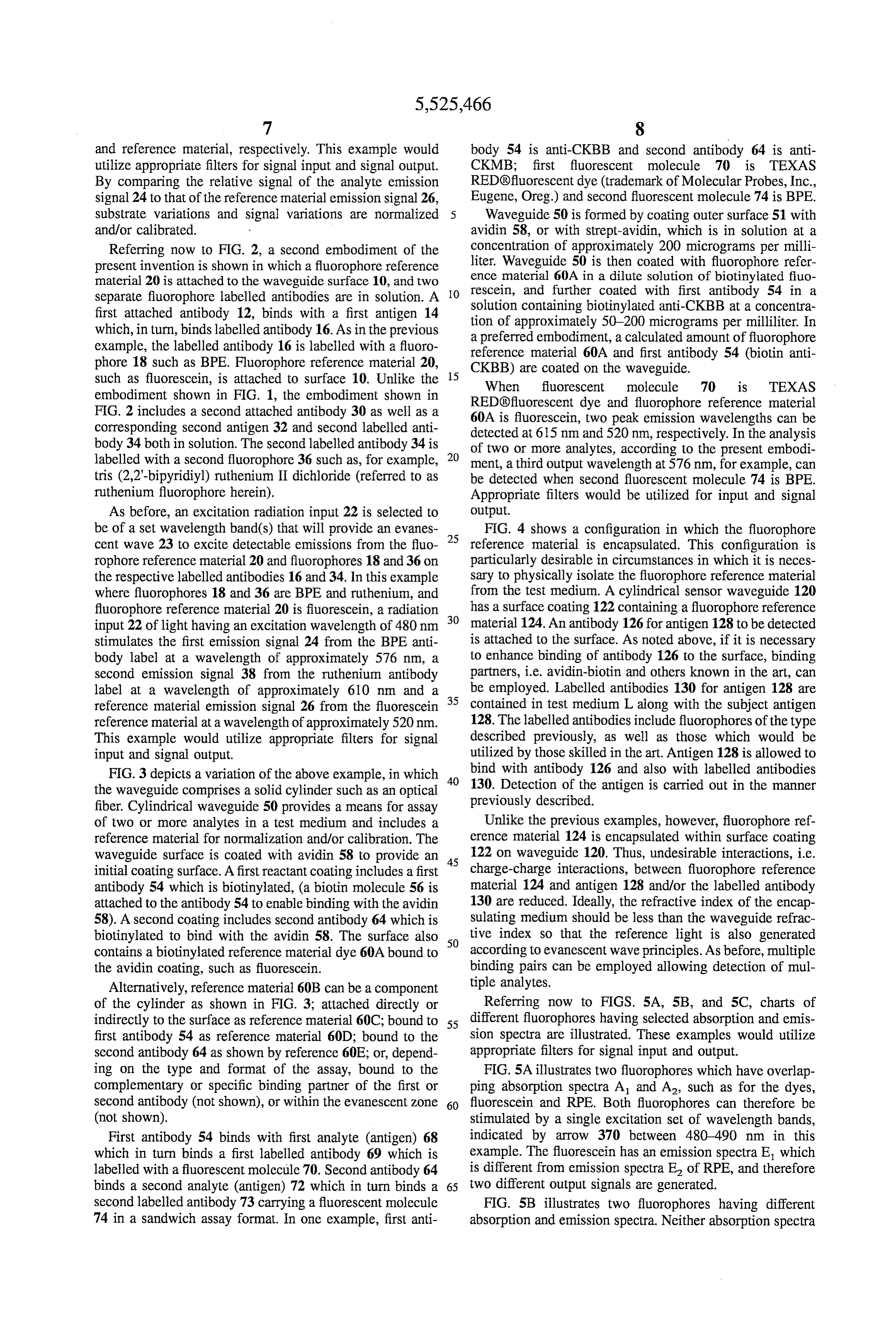
the reference material in the same manner as the signal from FIG. 1 is a schematic view of a portion of an evanescent the analyte, a ratio of the output of the analyte signal to the wave sensor having a single analyte binding partner coated output of the reference signal provides a value that will vary 15 thereon and showing various formats of interactions of the only with differences in the analyte and not with differences reference material at the evanescent Zone. between sensors. To avoid difficulty in the analysis of the FIG. 2 is a schematic view of a portion of an evanescent output signals, the reference material must be selected to wave sensor having a reference material and two analyte provide an output signal wavelength that is different and/or binding partners coated thereto. readily distinguishable from the signal that is indicative or 20 representative of the analyte. The reference material is used FIG. 3 is a schematic view of a portion of a cylindrical for signal normalization and/or calibration of the system in evanescent wave sensor having a reference material and two order to provide accurate and precise test results; and may be analyte binding partners bound to the surface via avidin. measured prior to, during or after the analyte measured FIG. 4 is a schematic view of a portion of a cylindrical signal. 25 evanescent wave sensor having a reference material encap Further advantages and objectives of the reference mate sulated in a coating on the sensor. rial include testing the effects of aging on the reactant FIG. 5A is a graph of intensity versus wavelength show coating; correlation of substrate and coating variability ing overlapping absorption or excitation wavelengths and between sensors in a given manufacturing batch, lot, or two different emission wavelengths. assay; and examining variations due to sensor manufacture 30 FIG. 5B is a graph of the spectra of two fluorophores or handling during coating. The use of the reference material having different absorption and emission wavelengths. further provides the advantages of detecting defective sen FIG. SC is a graph of the overlapping spectra of the sors i.e. a waveguide having a wave propagating surface emission wavelength of a first fluorophore and the absorp irregularity, including for example a scratch or chip. tion wavelength of a second fluorophore. In a second embodiment of the invention, multiple ana 35 FIG. 6A is a schematic view of an evanescent wave sensor lytes can be sensed or detected using a single sensor. One or having a diameter that increases in the distal direction. more wave propagating surfaces may be utilized for various FIG. 6B is a schematic view of an evanescent wave sensor assay formats. In one example of this embodiment, the test having a diameter that decreases in the distal direction. sample to be analyzed will contain two or more antibodies 40 specific for two or more analyte antigens, in which two or FIG. 7 is a schematic view of an evanescent wave sensor more of the antibodies are labelled with fluorophores that having a surface defect.
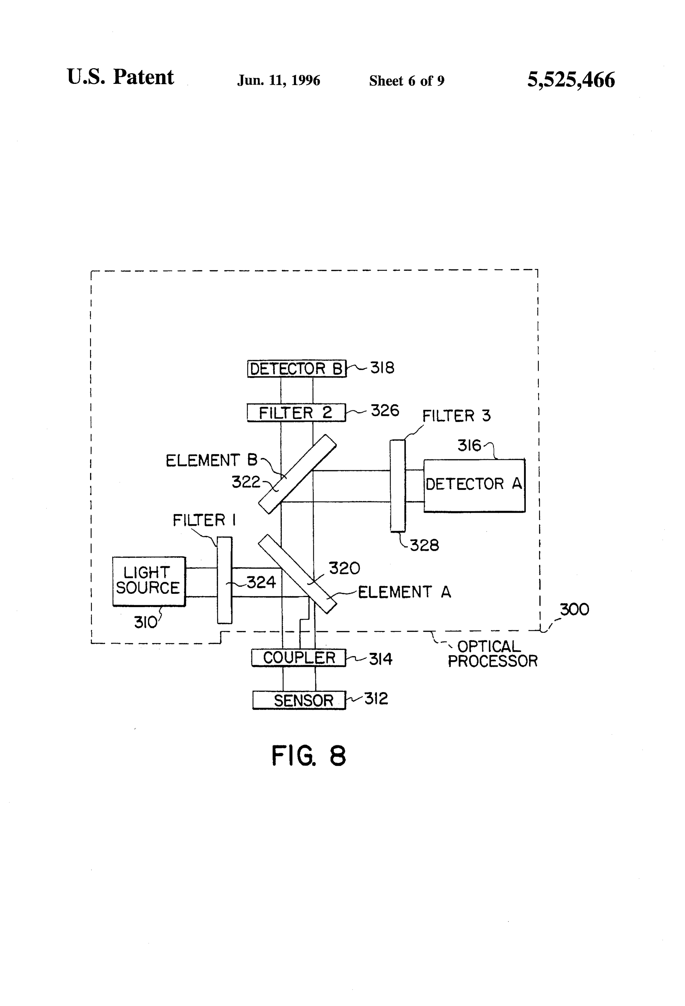
emit distinguishable output wavelengths or signals on eXpo FIG. 8 is a schematic representation of a system according sure to the evanescent wave. Two or more antibodies also to the invention.
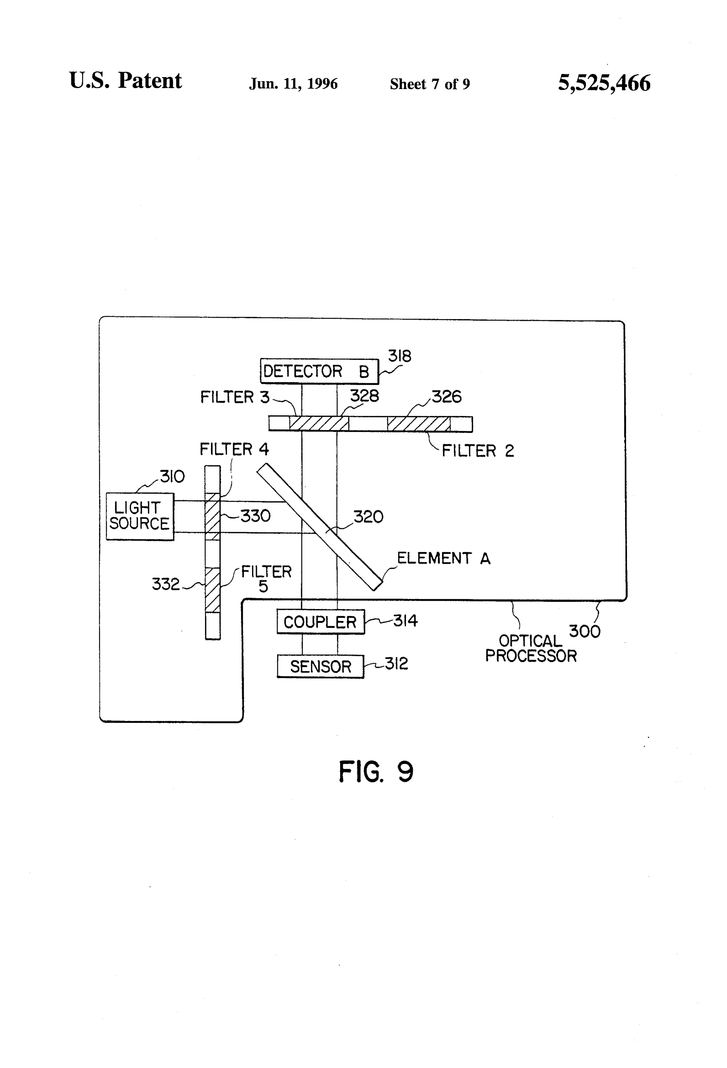
specific for the analyte antigens are attached to the surface. FIG. 9 is a schematic representation of another system If determination of only the relative amounts of the indi 45 according to the invention.
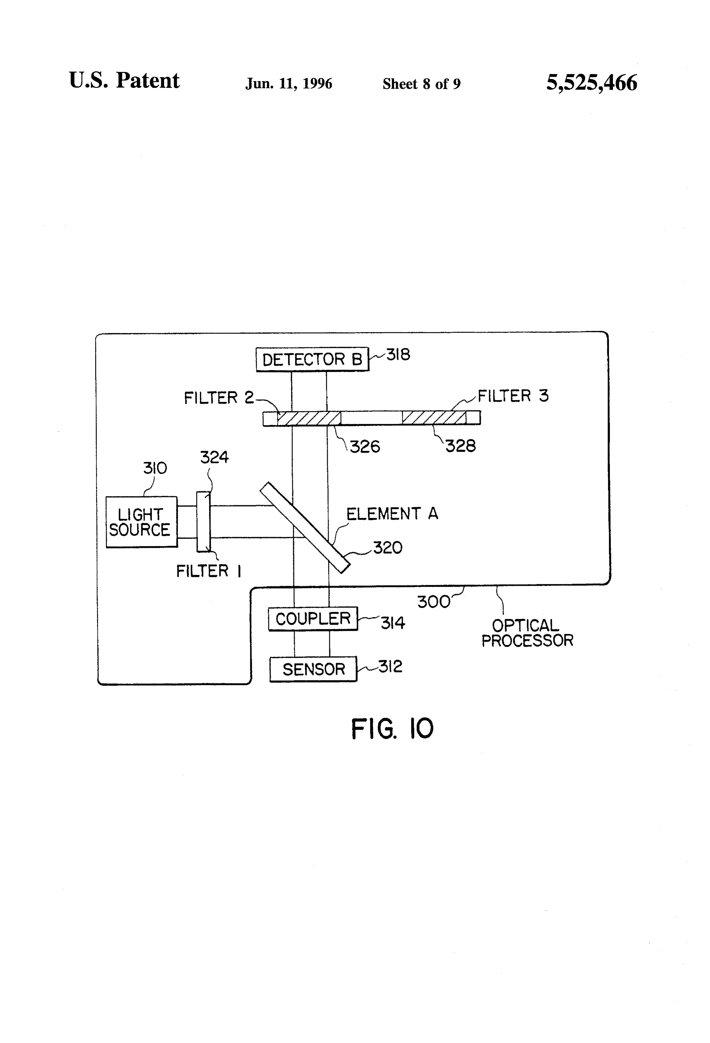
vidual analyte antigens is desired, this value can be directly FIG. 10 is a schematic representation of another system determined by comparing the individual output signals. according to the invention.
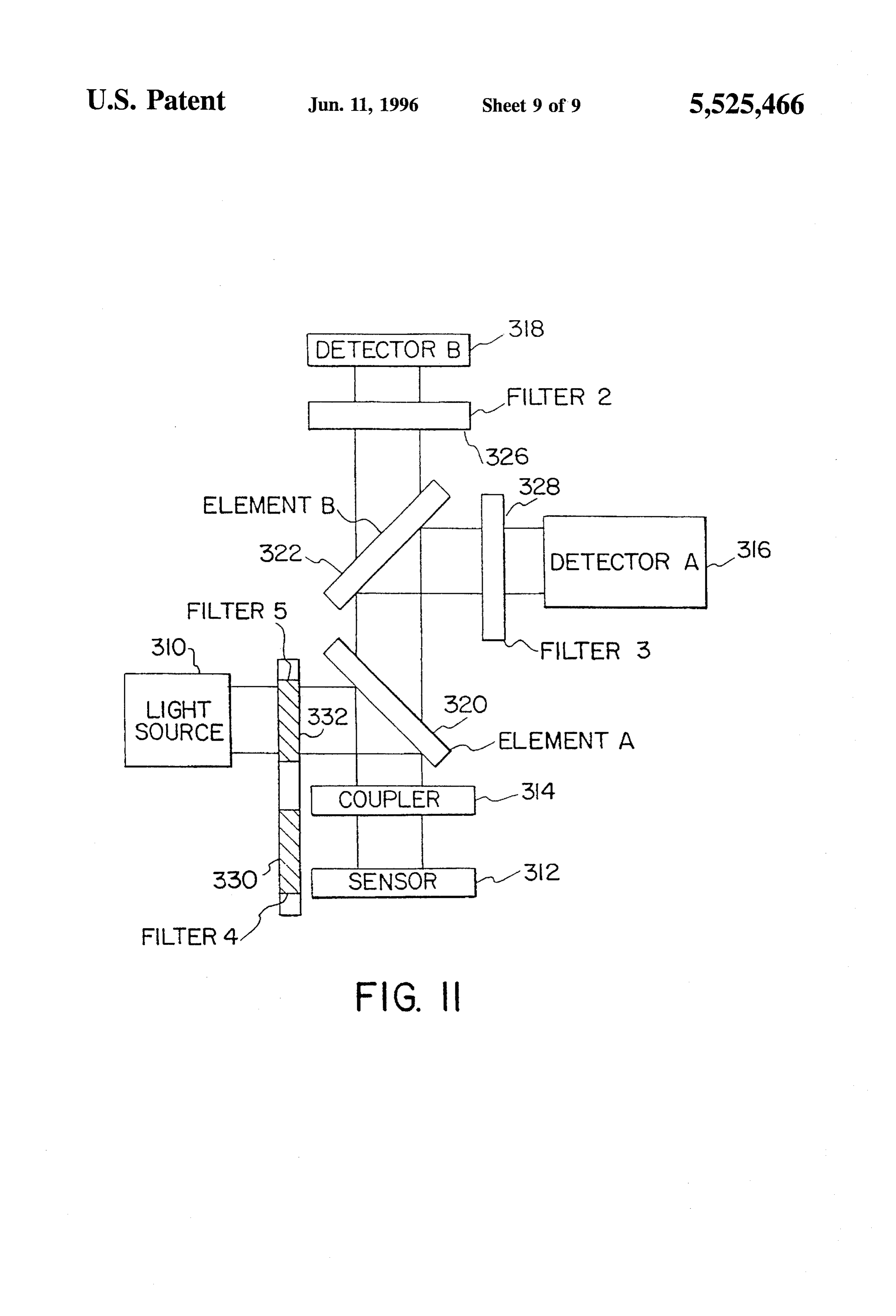
Alternatively, if an absolute analyte value is desired, a FIG. 11 is a schematic representation of another system reference material, as described above, can in one embodi 50 according to the invention.
ment of the invention be incorporated onto the same wave propagating surface from which the analyte is sensed. The reference material must be selected to provide an output DETAILED DESCRIPTION OF THE signal wavelength that is distinguishable from the output INVENTION wavelength of each of the fluorophores. 55 An evanescent wave system is described including a In a third embodiment of the invention, an assay can be Sensor, reference material and an operation means, and a performed in which the two analyte fluorophores overlap in method for using the system. An optical processor is a their wavelength absorption and emission bands; provided component of the system. In one embodiment, the sensor that proper fluorescent molecules are selected for the indi comprises two planar parallel surfaces, whereas in a pre vidual analytes. 60 ferred embodiment, the sensor comprises a waveguide hav In a fourth embodiment of the invention the reference ing a wave propagating surface, as in the case of a fiber optic material is added to the test medium believed to contain the strand or cable.
analyte to be detected, and the evanescent reaction carried The sensor receives a radiation input and emits one or out as described above. more output signals indicative of the presence of one or In a fifth embodiment of the invention, the reference 65 more analytes and a reference material in the evanescent material is used as a reference material for itself. In an Wave region (Harrick, infra and Love et al., infra). In the example of this embodiment, a fluorophore reference mate Case of a waveguide, the wave propagating surface is
Page 13
S 6 capable of receiving a radiation to excite a reference mate Other organic polymeric materials such as silicones, acry rial, the same radiation, if desired, also exciting at least one lates, fluoroacrylates, and the like can also be used as the analyte or receiving a second sequential or simultaneous sensor composition material. It is also desirable for the radiation to excite at least one analyte complex. The material to have negligible inherent fluorescence at the sequence of introducing radiation to excite the reference radiation wavelengths of interest for assays involving fluo material or analyte may be varied as necessary in the rescence. Other polymers and glass compositions would practice of various test methods. become apparent to those skilled in the art for application to In the case of the sensor having two separate parallel, various embodiments of this invention. planar surfaces, the input light is propagated between the Additionally, it is desirable for the composition material two surfaces. A single surface is capable of receiving at least 10 to have suitable surface properties for attachment of reactant a first radiation input and generating a signal output indica coating(s), including binding partners and reference mate tive of the presence of a reference material as well as a rials, to it or to be made suitable or amendable to modifi radiation output signal indicative of the presence of at least cation to assist attachment. PMMA is the preferred embodi one analyte. ment material not only for its optical purity and its injection One characteristic of the invention is that the evanescent 5 molding characteristics, but also because it is hydrophobic wave electromagnetic fields generated at the wave propa which enables antibodies and other molecules to be attached gating surface interact with one or more analytes at the or absorbed to the surface simply by bringing them in interface between the waveguide and a test medium. Test contact with the PMMA. For glass, it is desirable to provide mediums may include a gas, liquid or solid. In one configu either a hydrophobic surface or one amendable to covalent ration, for example, the wave propagating surface is coated and non-covalent coupling chemistries. with a reactant coating complementary or specific to at least A reactant coating as used herein shall be understood to one analyte and coated with a reference material that absorbs include the attachment by coating means of a molecule light in a set of wavelength bands and emits light at a which is receptive to a complementary molecule in a test different set of wavelength bands. The reference material 25 medium to form a binding pair. Binding pairs include includes fluorophores, chemiluminescent materials, time antibody-antigen, biotin-avidin and such other known sub resolved fluorophores and luminescent compounds. In one stances which have a homologous substance as are known in example, the reactant coating of the wave propagating the art. Coating as used herein shall be understood to include surface binds at least one analyte which in turn binds a specific and nonspecific reactions including non-covalent homologous binding partner carrying a fluorescent mol 30 binding and covalent binding.
ecule. The binding partner and the reference material may be Referring to FIG. 1, an example of the present invention, attached to the surface simultaneously or sequentially by in which a first fluorophore is attached to a surface 10 and covalent or non-covalent means. In another configuration a second fluorophore becomes attached to the surface is only an analyte binding partner is attached to the surface; shown. A first bound antibody 12 binds analyte antigen 14 with the reference material being added to the test medium. 35 which in turn binds labelled antibody 16. The labelled A fluorophore reference material and the fluorescent antibody 16 is labelled by means of a fluorophore 18. In one labelled molecule can be selected so that both are excited by example, the fluorophore 18 is B-phycoerythrin (BPE). A a set of wavelength bands and yet each emit an output signal fluorophore reference material 20A, such as fluorescein, is at a different wavelength. Appropriate filters, if necessary, attached to the surface 10.
for signal input and signal output would be utilized in the 40 Analyte, as used herein, shall be understood to include apparatus to practice the invention as described below. The any of a variety of chemical and biochemical substances. two different emitted fluorescent radiation wavelength(s) The use of the term analyte herein shall be understood to reenter the waveguide and are detected to enable accurate include both its singular tense and plural tense as appropri determination of the presence or quantity of one or more ate. The analyte sources may include physiological., scien analytes. These configurations and a number of alternative 45 tific and industrial (toxic and nontoxic) test mediums; where configurations are described in more detail below or will the presence, absence or quantity of the analyte in the become apparent to those skilled in the arts. medium is sought; and where, for example, analysis of a As stated above, there are a number of different configu physiological analyte is relevant to diagnosis and treatment rations of an evanescent wave sensor to provide one or more of a disease. Antibody as used herein shall be understood to wave propagating surfaces. One configuration involves a 50 include Fab antigen binding fragments, univalent fragments planar plate such as a microscope slide. Alternatively, a Fab' and bivalent fragments F(ab')2. second configuration involves a hollow waveguide; while Alternatively, the fluorophore reference material may be the third may be one as described in Slovaceket al., U.S. Pat. incorporated between two surfaces by reference 20B; or No. 5,156,976 entitled "Evanescent Wave Sensor Shell and within the evanescent zone as shown by reference 200; or as Apparatus' and; a fourth and preferred construction is that 55 a component or label of the reactant coating as shown by of a solid cylinder such as a waveguide, and more particu reference 20D.
larly an optical fiber. An excitation radiation input 22 is selected to excite There are several factors to be considered in selecting a emission within the evanescent wave zone from both the composition material for the sensor. One factor is that the fluorophore reference material 20A-D and the fluorophore material must have an index of refraction greater than that of 60 18 on labelled antibody 16. When fluorophores 18 are BPE the intended medium to be analyzed. Additionally, it is and fluorophore reference materials 20A-D are fluorescein, desirable for the material to be optically pure and provide a radiation input 22 of light having an excitation wavelength low attenuation of the radiation of interest. Silica glass is of 480 nm excites, via an evanescent wave 23, a first suitable for ultraviolet or visible radiation, plastics such as emission signal 24 from the BPE antibody label at a wave polymethylmethacrylate (PMMA), polystyrene, and poly 65 length of approximately 576 mm and a reference material carbonate are suitable for visible radiation, and fluoride emission signal 26 from the fluorescein reference material at glass or chalcogenide are suitable for near infrared radiation. a wavelength of approximately 520 nm to determine analyte
Page 14
and reference material, respectively. This example would body 54 is anti-CKBB and second antibody 64 is anti utilize appropriate filters for signal input and signal output. CKMB; first fluorescent molecule 70 is TEXAS By comparing the relative signal of the analyte emission REDQfluorescent dye (trademark of Molecular Probes, Inc., signal 24 to that of the reference material emission signal 26, Eugene, Oreg.) and second fluorescent molecule 74 is BPE. substrate variations and signal variations are normalized Waveguide 50 is formed by coating outer surface 51 with and/or calibrated. avidin 58, or with strept-avidin, which is in solution at a Referring now to FIG. 2, a second embodiment of the concentration of approximately 200 micrograms per milli present invention is shown in which a fluorophore reference liter. Waveguide 50 is then coated with fluorophore refer material 20 is attached to the waveguide surface 10, and two ence material 60A in a dilute solution of biotinylated fluo separate fluorophore labelled antibodies are in solution. A rescein, 10 and further coated with first antibody 54 in a solution containing biotinylated anti-CKBB at a concentra first attached antibody 12, binds with a first antigen 14 tion of approximately 50–200 micrograms per milliliter. In which, in turn, binds labelled antibody 16. As in the previous a preferred embodiment, a calculated amount of fluorophore example, the labelled antibody 16 is labelled with a fluoro reference material 60A and first antibody 54 (biotin anti phore 18 such as BPE. Fluorophore reference material 20, CKBB) are coated on the waveguide. such as fluorescein, is attached to surface 10. Unlike the 15
When fluorescent molecule 70 is TEXAS embodiment shown in FIG. 1, the embodiment shown in
FIG. 2 includes a second attached antibody 30 as well as a RED(E)fluorescent 60A is fluorescein, dye and fluorophore reference material two peak emission wavelengths can be corresponding second antigen 32 and second labelled anti detected at 615 nm and 520 nm, respectively. In the analysis body 34 both in solution. The second labelled antibody 34 is 20 of two or more analytes, according to the present embodi labelled with a second fluorophore 36 such as, for example, ment, a third output wavelength at 576 nm, for example, can tris (2,2'-bipyridiyl) ruthenium II dichloride (referred to as be detected when second fluorescent molecule 74 is BPE. ruthenium fluorophore herein). Appropriate filters would be utilized for input and signal As before, an excitation radiation input 22 is selected to output.
be of a set wavelength band(s) that will provide an evanes 25 FIG. 4 shows a configuration in which the fluorophore cent wave 23 to excite detectable emissions from the fluo reference material is encapsulated. This configuration is rophore reference material 20 and fluorophores 18 and 36 on particularly desirable in circumstances in which it is neces the respective labelled antibodies 16 and 34. In this example sary to physically isolate the fluorophore reference material where fluorophores 18 and 36 are BPE and ruthenium, and from the test medium. A cylindrical sensor waveguide 120 fluorophore reference material 20 is fluorescein, a radiation has a surface coating 122 containing a fluorophore reference input 22 of light having an excitation wavelength of 480 nm 30 material 124. An antibody 126 for antigen 128 to be detected stimulates the first emission signal 24 from the BPE anti is attached to the surface. As noted above, if it is necessary body label at a wavelength of approximately 576 nm, a to enhance binding of antibody 126 to the surface, binding second emission signal 38 from the ruthenium antibody partners, i.e. avidin-biotin and others known in the art, can label at a wavelength of approximately 610 nm and a 35 be employed. Labelled antibodies 130 for antigen 128 are reference material emission signal 26 from the fluorescein contained in test medium L along with the subject antigen reference material at a wavelength of approximately 520 nm. 128. The labelled antibodies include fluorophores of the type This example would utilize appropriate filters for signal described previously, as well as those which would be input and signal output. utilized by those skilled in the art. Antigen 128 is allowed to FIG.3 depicts a variation of the above example, in which 40 bind with antibody 126 and also with labelled antibodies the waveguide comprises a solid cylinder such as an optical 130. Detection of the antigen is carried out in the manner fiber. Cylindrical waveguide 50 provides a means for assay previously described.
of two or more analytes in a test medium and includes a Unlike the previous examples, however, fluorophore ref reference material for normalization and/or calibration. The erence material 124 is encapsulated within surface coating waveguide surface is coated with avidin 58 to provide an 45 122 on waveguide 120. Thus, undesirable interactions, i.e. initial coating surface. A first reactant coating includes a first charge-charge interactions, between fluorophore reference antibody 54 which is biotinylated, (a biotin molecule 56 is material 124 and antigen 128 and/or the labelled antibody attached to the antibody 54 to enable binding with the avidin 130 are reduced. Ideally, the refractive index of the encap 58). A second coating includes second antibody 64 which is sulating medium should be less than the waveguide refrac biotinylated to bind with the avidin 58. The surface also 50 tive index so that the reference light is also generated contains a biotinylated reference material dye 60A bound to according to evanescent wave principles. As before, multiple the avidin coating, such as fluorescein. binding pairs can be employed allowing detection of mul Alternatively, reference material 60B can be a component tiple analytes.
of the cylinder as shown in FIG. 3; attached directly or Referring now to FIGS. 5A, 5B, and 5C, charts of indirectly to the surface as reference material 60C; bound to 55 different fluorophores having selected absorption and emis first antibody 54 as reference material 60D; bound to the sion spectra are illustrated. These examples would utilize second antibody 64 as shown by reference 60E, or, depend appropriate filters for signal input and output. ing on the type and format of the assay, bound to the FIG. 5A illustrates two fluorophores which have overlap complementary or specific binding partner of the first or ping absorption spectra A and A2, such as for the dyes, second antibody (not shown), or within the evanescent Zone 60 fluorescein and RPE. Both fluorophores can therefore be (not shown). stimulated by a single excitation set of wavelength bands, First antibody 54 binds with first analyte (antigen) 68 indicated by arrow 370 between 480–490 nm in this which in turn binds a first labelled antibody 69 which is example. The fluorescein has an emission spectra E which labelled with a fluorescent molecule 70. Second antibody 64 is different from emission spectra E of RPE, and therefore binds a second analyte (antigen) 72 which in turn binds a 65 two different output signals are generated. second labelled antibody 73 carrying a fluorescent molecule FIG. 5B illustrates two fluorophores having different 74 in a sandwich assay format. In one example, first anti absorption and emission spectra. Neither absorption spectra
Page 15
A nor emission spectra E overlap with second absorption the diameter of the waveguide progressing in the direction of spectra A or the emission spectra E of a second fluoro the radiation input wave. The sensor has a fluorophore phore. In one example, the first fluorophore is fluorescein reference material 152 and an antibody 154 attached thereto. and the second fluorophore is TEXAS REDG) fluorescent Test medium L contains an antigen 156 to be analyzed and dye. a labelled antibody 158 which can bind antigen 156 in a FIG. 5C illustrates two fluorophores in which the emis sandwich assay format. A light input 160 produces an sion spectra E overlaps the absorption spectra A of the waveevanescent wave 162 at each region of contact 164 with the propagating surface. Evanescent wave 162 stimulates second fluorophore. One such set of dyes is fluorescein and an emission
BPE. Other combinations include BPE and TEXAS signal 166 from labelled antibodies 158 which RED(Efluorescent dye or C-phycoeyanin and TEXAS 10 are bound to antigens 156 bound to antibody 154 on the waveguide. Evanescent wave 162 also stimulates emission
REDQfluorescent dye. of a reference signal 168 from fluorophore reference mate Therefore, it can be seen that a number of dye combina rial 152 attached to the waveguide. Alternatively, fluoro tions can be used with the embodiments of the present phore reference material 152 may interact with the invention in the use of one or more wave propagating 15 waveguide as described above.
surfaces. In addition, one or more dyes may be used as The signal output of the evanescent waves 162 varies reference materials. A partial listing of suitable dyes is partially in proportion to the number of bounces (reflec presented in TABLE I. The use of alternate dyes and dye tions), or contacts 164, with the waveguide surface. How combinations to practice the invention as described herein ever, for a waveguide of increasing diameter (as in FIG. 6A), will be apparent to those skilled in the art. it is seen that the number of contacts 164 will decrease per
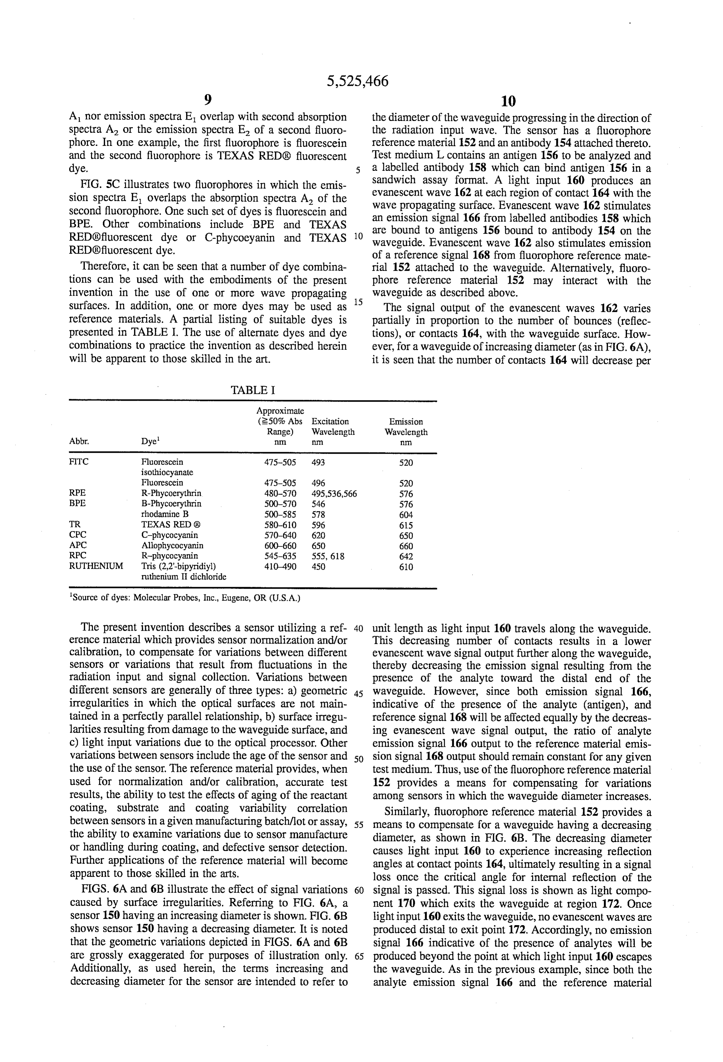
TABLE I
Approximate (250% Abs Excitation Emission
Range) Wavelength Wavelength
Fluorescein 475-505. 493 520 isothiocyanate
Fluorescein 475-505 496 520
R-Phycoerythrin 480-570 495,536,566 576
B-Phycoerythrin 500-570 546 576 rhodamine B 500-585 578 604
TEXAS RED (8) 580-610 596 615
C-phycocyanin 570-640 620 650
Allophycocyanin 600-660 650 660
R-phycocyanin 545-635 555, 618 642
Tris (2,2'-bipyridiyl) 410.490 450 610 ruthenium II dichloride
'Source of dyes: Molecular Probes, Inc., Eugene, OR (U.S.A.)
The present invention describes a sensor utilizing a ref 40 unit length as light input 160 travels along the waveguide. erence material which provides sensor normalization and/or This decreasing number of contacts results in a lower calibration, to compensate for variations between different evanescent wave signal output further along the waveguide, sensors or variations that result from fluctuations in the thereby decreasing the emission signal resulting from the radiation input and signal collection. Variations between presence of the analyte toward the distal end of the different sensors are generally of three types: a) geometric 45 waveguide. However, since both emission signal 166, irregularities in which the optical surfaces are not main indicative of the presence of the analyte (antigen), and tained in a perfectly parallel relationship, b) surface irregu reference signal 168 will be affected equally by the decreas larities resulting from damage to the waveguide surface, and ing evanescent wave signal output, the ratio of analyte c) light input variations due to the optical processor. Other emission signal 166 output to the reference material emis variations between sensors include the age of the sensor and 50 sion signal 168 output should remain constant for any given the use of the sensor. The reference material provides, when test medium. Thus, use of the fluorophore reference material used for normalization and/or calibration, accurate test 152 provides a means for compensating for variations results, the ability to test the effects of aging of the reactant among sensors in which the waveguide diameter increases. coating, substrate and coating variability correlation Similarly, fluorophore reference material 152 provides a between sensors in a given manufacturing batch/lot or assay, 55 means to compensate for a waveguide having a decreasing the ability to examine variations due to sensor manufacture diameter, as shown in FIG. 6B. The decreasing diameter or handling during coating, and defective sensor detection. causes light input 160 to experience increasing reflection Further applications of the reference material will become angles at contact points 164, ultimately resulting in a signal apparent to those skilled in the arts. loss once the critical angle for internal reflection of the FIGS. 6A and 6B illustrate the effect of signal variations 60 signal is passed. This signal loss is shown as light compo caused by surface irregularities. Referring to FIG. 6A, a ment 170 which exits the waveguide at region 172. Once sensor 150 having an increasing diameter is shown. FIG. 6B light input 160 exits the waveguide, no evanescent waves are shows sensor 150 having a decreasing diameter. It is noted produced distal to exit point 172. Accordingly, no emission that the geometric variations depicted in FIGS. 6A and 6B signal 166 indicative of the presence of analytes will be are grossly exaggerated for purposes of illustration only. 65 produced beyond the point at which light input 160 escapes Additionally, as used herein, the terms increasing and the waveguide. As in the previous example, since both the decreasing diameter for the sensor are intended to refer to analyte emission signal 166 and the reference material
Page 16
emission signal 168 will be affected equally by the loss of Element B (322) – Dichroic that transmits the emission light input 160 beyond a certain point on the waveguide, the light of one of the fluoromers being measured and ratio of emission signal 166 output to the reference material reflects the light emitted by the second fluoromer. (It is emission signal 168 output should remain constant for any noted that any standard beam splitter can be used but given test sample. The use of fluorophore reference material would reduce the SNR).
152 provides a means for compensating for variations among sensors in which the waveguide diameter decreases. Filter 1 (324) - Dual band interference filter for trans The effect of surface irregularities on a sensor is shown mitting the excitation light for the two fluoromers to be measured.
schematically in FIG. 7. It is noted that a sensor having a surface defect of any significance should be rejected for use O Filter 2 (326) - Interference filter that transmits the light in analyzing a medium for the presence of an analyte. The generated by one of the fluoromers. sensor should optimally be pretested with a reference mate Filter 3 (328) - Interference filter that transmits the light rial before contact with a test sample. In the preferred generated by the second fluoromer. embodiment the reference material will be attached to the The following elements are only used in FIGS. 9 and 11) sensor/br pretesting purposes. 15 Filter 4 (330) - Interference filter that transmits the In FIG. 7, a waveguide 180 contains a defect, or surface excitation light for the second fluoromer being mea irregularity 182. Light input 202 is internally reflected along sured.
the waveguide to produce evanescentradiation, however the reflection is effected by the surface irregularity 182. Such Filter 5 (332) - Interference filter that transmits the effects are undesirable because they reduce the production of excitation light for one of the fluoromers being mea evanescent waves 162 in the region distal to the defect, 20 sured.
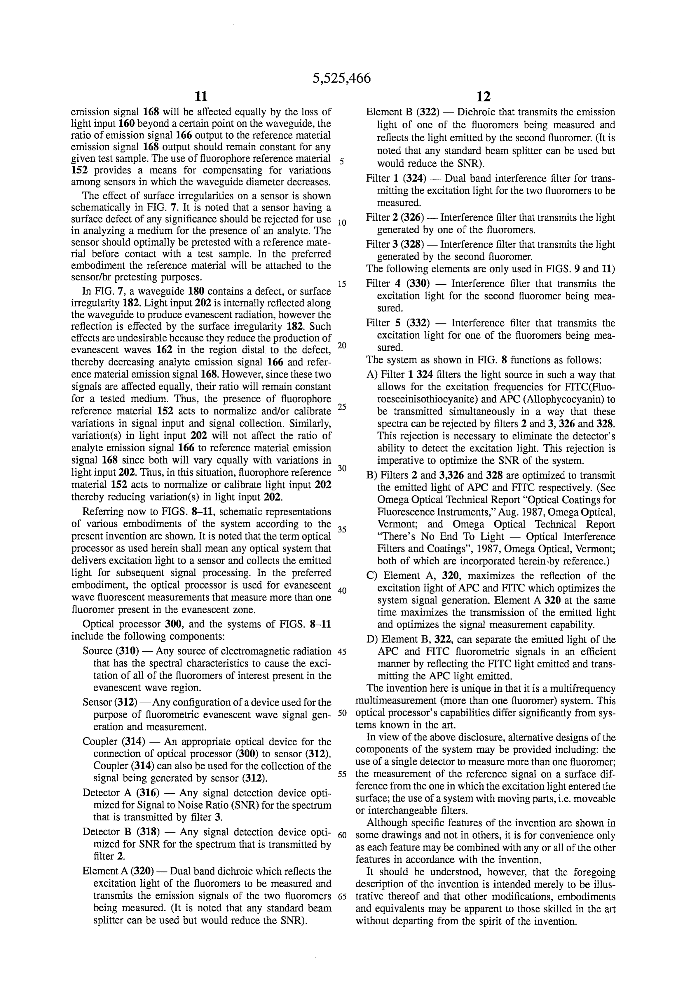
thereby decreasing analyte emission signal 166 and refer The system as shown in FIG. 8 functions as follows: ence material emission signal 168. However, since these two A) Filter 1324 filters the light source in such a way that signals are affected equally, their ratio will remain constant allows for the excitation frequencies for FITC(Fluo for a tested medium. Thus, the presence of fluorophore 25 roesceinisothiocyanite) and APC (Allophycocyanin) to reference material 152 acts to normalize and/or calibrate be transmitted simultaneously in a way that these variations in signal input and signal collection. Similarly, spectra can be rejected by filters 2 and 3,326 and 328. variation(s) in light input 202 will not affect the ratio of This rejection is necessary to eliminate the detector's analyte emission signal 166 to reference material emission ability to detect the excitation light. This rejection is signal 168 since both will vary equally with variations in imperative to optimize the SNR of the system. light input 202. Thus, in this situation, fluorophore reference 30 B) Filters 2 and 3,326 and 328 are optimized to transmit material 152 acts to normalize or calibrate light input 202 the emitted light of APC and FITC respectively. (See thereby reducing variation(s) in light input 202. Omega Optical Technical Report "Optical Coatings for Referring now to FIGS. 8-11, schematic representations Fluorescence Instruments,” Aug. 1987, Omega Optical, of various embodiments of the system according to the 35 Vermont; and Omega Optical Technical Report present invention are shown. It is noted that the term optical "There's No End To Light – Optical Interference processor as used herein shall mean any optical system that Filters and Coatings”, 1987, Omega Optical, Vermont; delivers excitation light to a sensor and collects the emitted both of which are incorporated herein by reference.) light for subsequent signal processing. In the preferred C) Element A, 320, maximizes the reflection of the embodiment, the optical processor is used for evanescent 40 excitation light of APC and FITC which optimizes the wave fluorescent measurements that measure more than one system signal generation. Element. A 320 at the same fluoromer present in the evanescent zone. time maximizes the transmission of the emitted light Optical processor 300, and the systems of FIGS. 8-11 and optimizes the signal measurement capability. include the following components: D) Element B, 322, can separate the emitted light of the Source (310) - Any source of electromagnetic radiation 45 APC and FITC fluorometric signals in an efficient that has the spectral characteristics to cause the exci manner by reflecting the FITC light emitted and trans tation of all of the fluoromers of interest present in the mitting the APC light emitted.
evanescent wave region. The invention here is unique in that it is a multifrequency Sensor (312) - Any configuration of a device used for the multimeasurement (more than one fluoromer) system. This purpose of fluorometric evanescent wave signal gen 50 optical processor's capabilities differ significantly from sys eration and measurement. tems known in the art.
Coupler (314) - An appropriate optical device for the In view of the above disclosure, alternative designs of the connection of optical processor (300) to sensor (312). components of the system may be provided including: the Coupler (314) can also be used for the collection of the 55 use of a single detector to measure more than one fluoromer; signal being generated by sensor (312). the measurement of the reference signal on a surface dif Detector A (316) - Any signal detection device opti ference from the one in which the excitation light entered the mized for Signal to Noise Ratio (SNR) for the spectrum Surface; the use of a system with moving parts, i.e. moveable or interchangeable filters.
that is transmitted by filter 3. Although specific features of the invention are shown in Detector B (318) - Any signal detection device opti 60 some drawings and not in others, it is for convenience only mized for SNR for the spectrum that is transmitted by as each feature may be combined with any or all of the other filter 2. features in accordance with the invention. Element A (320) - Dual band dichroic which reflects the It should be understood, however, that the foregoing excitation light of the fluoromers to be measured and description of the invention is intended merely to be illus transmits the emission signals of the two fluoromers 65 trative thereof and that other modifications, embodiments being measured. (It is noted that any standard beam and equivalents may be apparent to those skilled in the art splitter can be used but would reduce the SNR). without departing from the spirit of the invention.
Page 17
We claim: index of refraction substantially equal to the index of 1. An evanescent wave sensor for receiving one or more refraction of the test medium.
electromagnetic radiation input signals and emitting at least 13. The sensor of claim 1 wherein the molecular species two output signals, said sensor comprising: is selected from the group consisting of: a waveguide sensor having at least one wave propagating receptors and ligands.
surface including a reactant coating immobilized 14. The sensor of claim 1, when said sensor further thereon comprising molecular species that specifically comprises: an optical processor having a lens arranged to bind to an analyte that may be present in a test medium; launch light into the waveguide to generate evanescent wave and a fluorescent reference material which is attached to said 10 electromagnetic fields; and a detector for measuring light waveguide, wherein the sensor surface receives one or emitted from the wave guide to form a sensor system. more electromagnetic radiation input signals and emits 15. An evanescent wave sensor system for receiving one an output electromagnetic radiation signal dependent or more light input signals and emitting at least two output on the presence of at least one analyte and another signals, comprising:
output electromagnetic radiation signal from the fluo 15 a sensor having at least one wave propagating surface for rescent reference material; such that the reference propagating light input along the surface; said surface material provides for normalization and/or calibration including a reactant coating immobilized thereon hav of the sensor. ing a molecular species that specifically binds to a 2. The sensor of claim 1 wherein the molecular species is 20 molecule that may be present in a medium or test selected from the group consisting of: sample and a fluorescent reference material; wherein antigens, the surface is capable of receiving light input signals antibodies, and causing a reference output signal dependent on the reference material and an output signal dependent on amino acid sequences, and the presence of at least one molecule in said medium or nucleic acid sequences. 25 test sample; and wherein the reference material pro 3. The sensor of claim 1, wherein the waveguide com vides normalization and/or calibration of the system. prises two separate surfaces or a cone. 16. A method for analyzing a test medium comprising: 4. The sensor of claim 1 wherein the waveguide com propagating a light input along at least one wave propa prises a hollow waveguide. gating surface of a sensor; 5. The sensor of claim 1 wherein the waveguide com 30 contacting the wave propagating surface with said test prises an optical fiber. medium;
6. The sensor of claim 1 wherein the waveguide com prises a planar structure having opposed parallel surfaces. propagating light along the wave propagating surface to 7. The sensor of claim 1 wherein the electromagnetic generate evanescent wave electromagnetic fields at the radiation signal from the reference material is used to test the 35 surface to irradiate the test medium; and sensor for effects of storage or aging. detecting light reentering the wave propagating surface 8. The sensor of claim 1, wherein the signal from the and emitted from the wave propagating surface, reference material is used to correlate the variability wherein the surface has a reactant coating including a between sensors in a given manufacturing batch/lot or assay. fluorescent reference material and a binding partner of 9. The sensor of claim 1, wherein the signal from the 40 at least one analyte, said surface being capable of reference material is used to examine variations in excitation receiving the light input and causing a reference output and collection efficiency between waveguides due to signal dependent on the reference material, at least one waveguide manufacture or handling during coating. light output signal from a labelled species dependent on 10. The sensor of claim 1, wherein the signals from the the presence of at least on analyte and wherein the reference material is used to detect defective waveguides. 45 reference material provides for normalization and/or 11. The sensor of claim 1 further including means for calibration of the system.
isolating the fluorescent reference material from the analyte 17. The method of claim 16 in which detecting includes or molecular species, wherein said means for isolating monitoring at least a first output signal indicative of the includes encapsulation of said fluorescent reference material presence of at least a first analyte and a reference output within the reactant coating on the waveguide. 50 signal indicative of the presence of the reference material.
12. The sensor of claim 11 in which said means for isolating comprises an encapsulation material having an ck : :: *k sk
Provenance
- Collection
- Cited prior art
- Original PDF
- patentimages.storage.googleapis.com →
- Filed
- 1994-05-20
- Pages
- 17
- Method
- pdftotext (the PDF's own text layer) + pdftoppm 300dpi page scans
- Source
- Google Patents bibliographic record
- Granted
- 1996-06-11
- Inventors
- Rudolf E. Slovacek; Walter F. Love; Richard L. Schulkind; Irene M. Walczak; Thomas A. Cook; Ciba Corning Diagnosys Corp
- Transcribed from
- patentimages.storage.googleapis.com →