patent · US5340715
Multiple surface evanescent wave sensor with a reference
23 August 1994
Page 1 — bibliographic record
United States Patent 19 11) Patent Number: 5,340,715 Slovacek et al. (45) Date of Patent: Aug. 23, 1994 54 MULTIPLE SURFACE EVANESCENT WAVE 4,842,783 6/1989 Blaylock ............................... 385/12 SENSORWTH A REFERENCE 4,846,548 7/1989 Klainer .................................. 385/12 4,880,752 11/1989 Keck et al. ... ... 436/807 75 Inventors: Rudolf E. Slovacek, Norfolk, Mass.; 5,001,051 3/1991 Miller et al. ............................ 435/6 Walter F. Love, Horseheads; Thomas 5,156,976 10/1992 Slovacek et al. ................ 422/82.11 A. Cook, Corning, both of N.Y.;
Richard L. Schulkind, Sharon; Irene OTHER PUBLICATIONS
M. Walczak, Boston, both of Mass. Halliday et al., Physics, (John Wiley & Sons, New York), 73) Assignee: Ciba Corning Diagnostics Corp., 1978, p. 947.
Medfield, Mass. Primary Examiner-Toni R. Scheiner
O Assistant Examiner-Christopher L. Chin 21 Appl. No.: 711,783 Attorney, Agent, or Firm-Nicholas I. Slepchuk, Jr.; 22 Filed: Jun. 7, 1991 Arthur S. Morgenstern; Judith A. Roesler I51) Int. Cl. ........................................... GON 33/552 57 ABSTRACT 52 U.S. Cl. .......................................... 435/6; 422/57;
422/82.05; 422/82.07: 422/82.08: 422/82.11: An evanescent wave sensor and method for use in ana 435/174; 435/176; 435/1 82; 435/261. 435780s. lyzing one or more media, the sensor including a wave 436/164:436/172436/518.436/527.436/805. guide having first and second wave propagating Sur 436/807; 385/12;385/141; 385/142; 385/143 faces. The waveguide propagates an input signal along 58 Field of Search ................. 385/12, 141,142, 143; the waveguide between the first and second surfaces. 422/57, 82.05, 82.06, 82.07, 82.08, 82.09, 82.11; The first surface receives a first radiation signal which 435/6, 174, 176, 177, 180, 181, 182,291, 808; indicates the presence of a first analyte, and the second 436/518, 527, 164, 172,805, 807 Surface receives a second radiation signal representing one or both of a second analyte and a reference. The 56 References Cited first and second surfaces can both be contacted with a
4,050,895 9/1977 Hardy et al. ........................ 436/805 more output signals can be detected. 4,558,014 12/1985 Hirschfeld et al. ................. 436/808 4,775,637 10/1988 Sutherland et al. ............. 422/82.11 26 Claims, 10 Drawing Sheets
Page 2
Drawing sheet — no readable text.
Page 3
Drawing sheet — no readable text.
Page 4
Drawing sheet — no readable text.
Page 5
Drawing sheet — no readable text.
Page 6
Drawing sheet — no readable text.
Page 7
Drawing sheet — no readable text.
Page 8
Drawing sheet — no readable text.
Page 9
Drawing sheet — no readable text.
Page 10
Drawing sheet — no readable text.
Page 11
Drawing sheet — no readable text.
Page 12
critical angle is propagated through the optical wave
MULTIPLE SURFACE EVANESCENT WAVE guide to emerge from an output end. SENSORWTH A REFERENCE Several improved dielectric waveguides are de
FIELD OF THE INVENTION
scribed in U.S. Pat. No. 4,880,752; which is incorpo rated herein by reference. In one construction, the
This invention relates to improved evanescent wave waveguide has an elongated rod-shaped core having an sensors for use in spectrophotometric signal responsive opening within the core material. A reactant coating is processing assays of analytes in fluids, and more particu disposed about the opening within the core on a single larly to such sensors having at least two optical surfaces optical surface.
which carry one or more fluoromeres and/or a reactive 10 Presently, only a single analyte is analyzed in most coating. conventional procedures. There is, however, a need for CROSS-REFERENCES analyzing more than one analyte at a time, or for simul taneously examining a reference material to indicate
The following applications, filed concurrently with, fluctuations in light intensity, defects in the optical sur are incorporated herein by reference: Slovacek et al., 15 face of the sensor, and similar factors which may alter
Pat. No. 5,156,976, entitled “Evanescent Wave Sensor variation in diameter of wall thickness of a fiber optic Shell and Apparatus'; and Slovacek et al., U.S. patent rod changes the angle at which light is totally internally application Ser. No. 07/712,304 entitled "Multiple Out reflected, and may cause the radiation to eventually put Referencing System. For An Evanescent Wave 20 strike at an angle less than the critical angle, and there Sensor'. fore escape the sensor. Alternatively, if the angle be TECHNICAL DISCLOSURE comes increasingly greater than the critical angle, there will be fewer reflections which reduces the amount of
There are a number of optical devices which propa evanescent wave electromagnetic fields which are de gate radiation by total internal reflection to generate an 25 livered to the surrounding medium. evanescent wave at the interface of the device and a A number of immunoassay technique formats are surrounding medium having a lower index of refraction. known in the art may be practiced with the sensors of See Harrick, N.J., Internal Reflection Spectroscopy, the present invention.
Hatrick Scientific Corp., Ossinging, N.Y. (Third Print ing 1987). The evanescent wave is an electromagnetic 30 SUMMARY OF THE INVENTION waveform which typically extends less than a wave The evanescent wave sensor of the invention has a length into the surrounding medium. However, this penetration is sufficient to permit substantial optical iswaveguide propagated with at least two optical surfaces. Radiation along the waveguide between the first interaction between the evanescent wave component and second surfaces by total internal reflection. The and one or more target substances in the medium. 35
One use of optical devices is in the area of fluorescent first surface receives a radiation signal which indicates immunoassays. Presently, optical waveguides in the the presence of a first analyte in a medium and the sec form of fiber optic rods typically are coated with either ond surface receives a radiation signal representing one an antibody or an antigen which binds the correspond or both of a second analyte and/or a reference. The ing antigen or antibody, respectively, suspected of 40 sequence and number of radiation signals may vary being present in a medium or test sample. This coating depending on the type of analyses being performed by typically is applied prior to the performance of an im the sensor and the fluorescent tags employed with the munoassay measurement. In a 'sandwich' immunoas assay. The sensor therefore is capable of detecting one say, an antibody is bound to the surface of the fiber or more analytes in a single medium, detecting simulta optic rod to form a reactant coating, and the device is 45 neously one or more analytes in two different media, or subsequently immersed in a sample suspected of con detecting simultaneously an analyte and a reference. taining the antigen to be analyzed. Antigen present in Use of a reference provides an automatic indication of the sample binds with the attached antibody. A second fluctuations in light intensity, defects in the optical sur antibody, previously labelled by a fluorescent tag, is face of the sensor, or other factors which affect the added to the sample. Alternatively, in a "one-step' 50 apparent quantity of detected output radiation. assay, the second, labelled antibody is first mixed with In one embodiment, the waveguide is a hollow core the antigen in the sample, and the mixture is brought having an inner surface and an outer surface. One of the into contact with the fiber optic rod and the first, bound inner and outer surfaces forms the first wave propagat antibody. In either technique, the labelled antibody ing surface and the other of the inner and outer surfaces attaches to the antigen to form a tagged complex bound 55 forms the second wave propagating surface. Alterna to the fiber optic rod by the first antibody. tively, the waveguide is a shell having a radiation port Light is subsequently introduced into the fiber optic at a first end and a base at a second end, and having rod at one or more wavelengths and is propagated inner and outer wall surfaces extending between the along the fiber optic rod by total internal reflection. The radiation port and the base to form the first and second reflection is, of course, not completely total since the wave propagating surfaces. One or both of the first and fluorescent tag absorbs a small amount of the radiation. second surfaces can carry a reactant coating which may The attached fluorescent tag (referred to as a fluoro include a binding partner of an analyte to be detected. phore) absorbs energy from the evanescent wave elec The reactant coating may include an immobilized anti tromagnetic fields at a first wavelength and fluoresces body, antigen, enzyme, nucleic acid, receptor, or other at a second, longer wavelength. Fluorescence from the 65 known binding molecules. When used for a fluorescent excited fluorophore passes into the optical waveguide immunoassay procedure, the waveguide is transmissive via a tunneling effect and the portion of the fluorescent to light which can excite fluorescence of fluorescent tag radiation which occurs at an angle greater than the and is transmissive to fluorescent radiation from the
Page 13
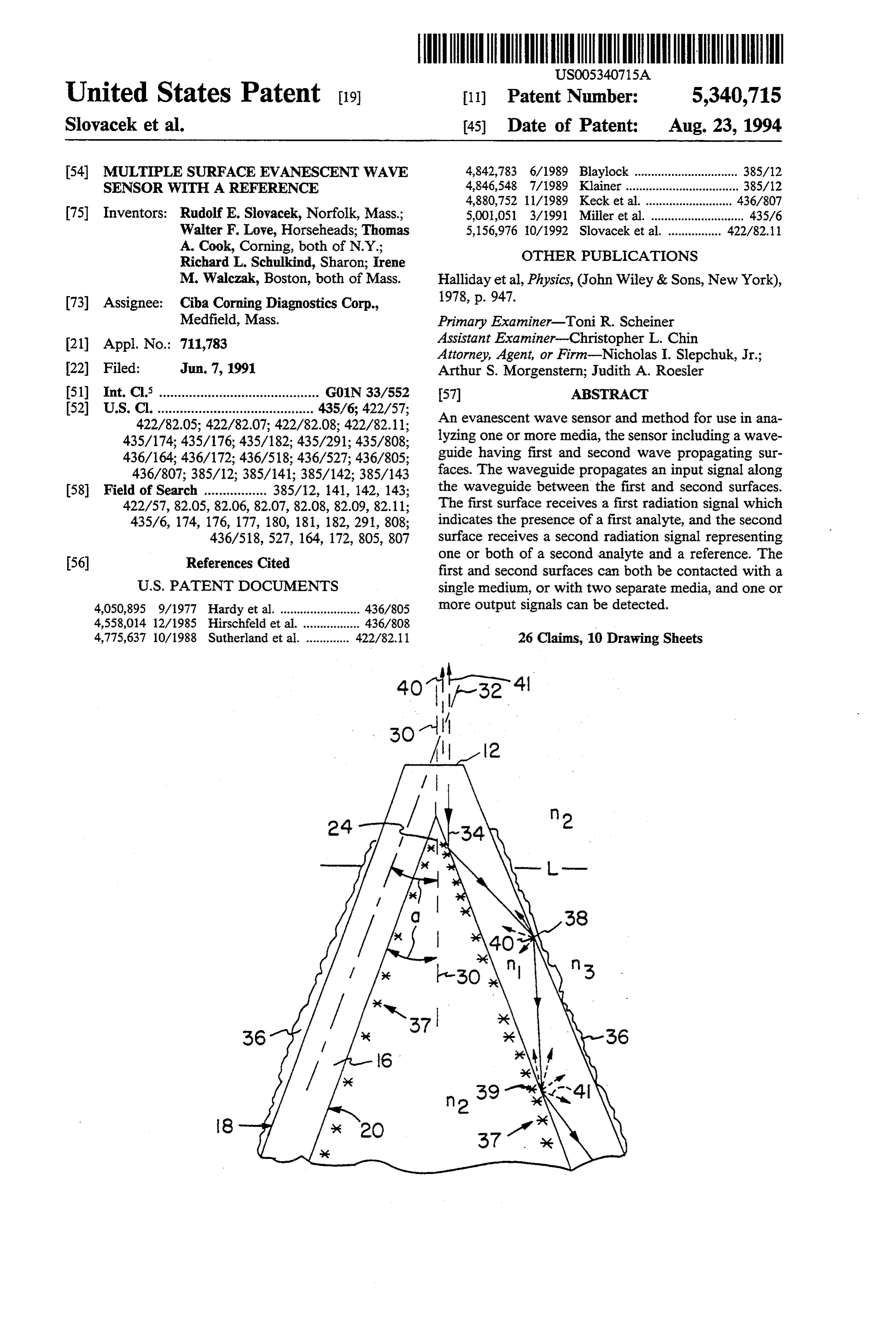
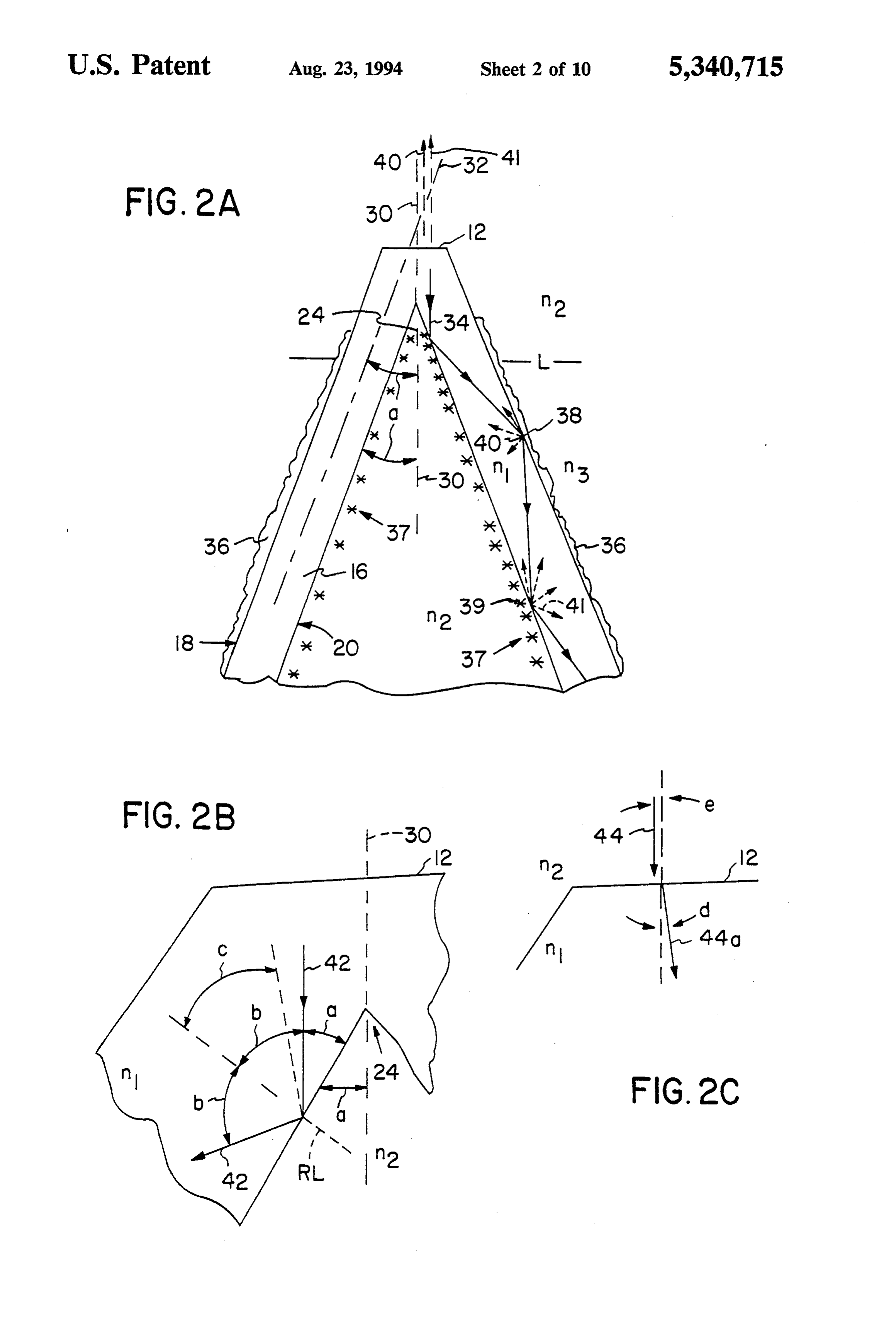
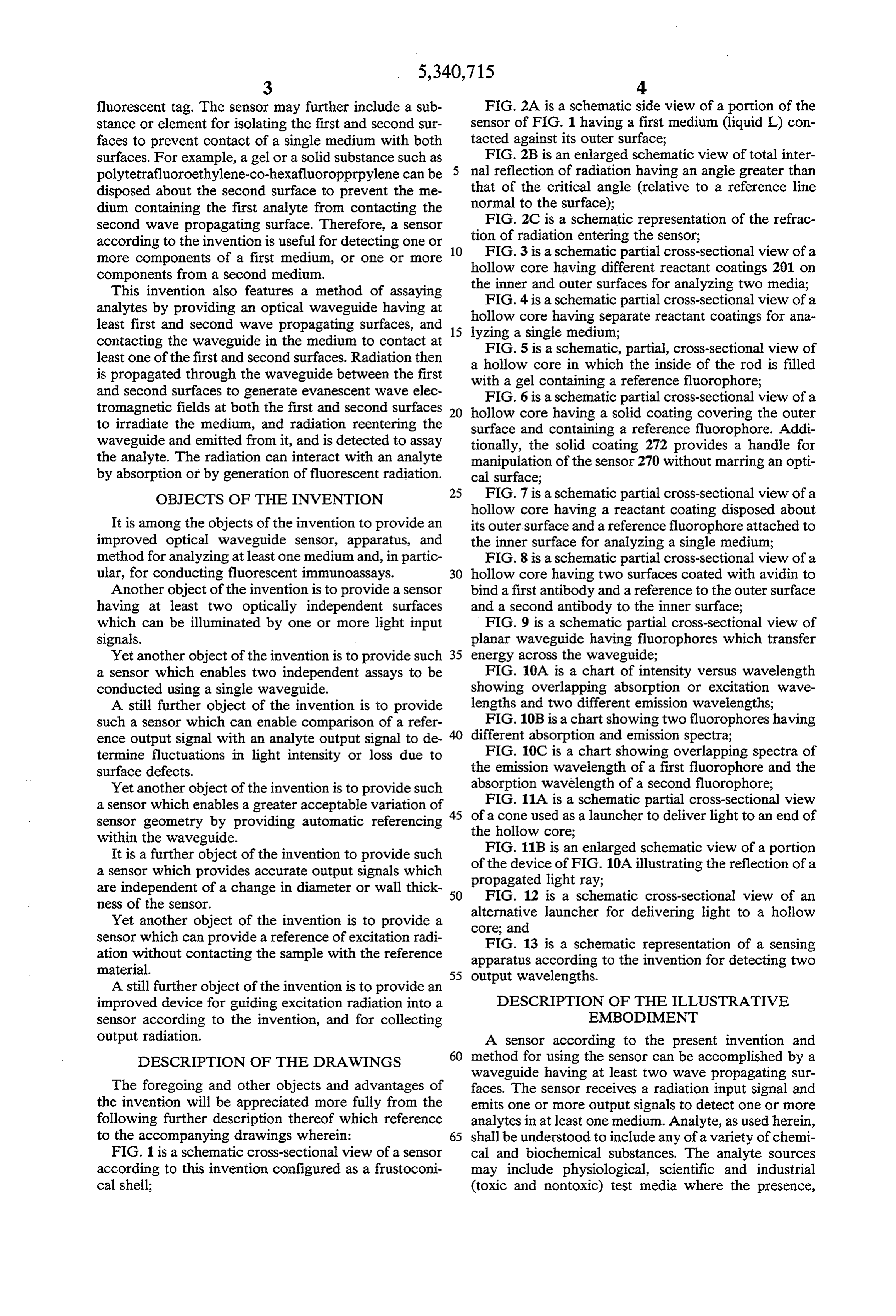
fluorescent tag. The sensor may further include a sub FIG. 2A is a schematic side view of a portion of the stance or element for isolating the first and second sur sensor of FIG. 1 having a first medium (liquid L) con faces to prevent contact of a single medium with both tacted against its outer surface;
surfaces. For example, a gel or a solid substance such as FIG. 2B is an enlarged schematic view of total inter polytetrafluoroethylene-co-hexafluoropprpylene can be nal reflection of radiation having an angle greater than disposed about the second surface to prevent the ne that of the critical angle (relative to a reference line dium containing the first analyte from contacting the normal to the surface);
second wave propagating surface. Therefore, a sensor tionFIG. 2C is a schematic representation of the refrac of radiation entering the sensor;
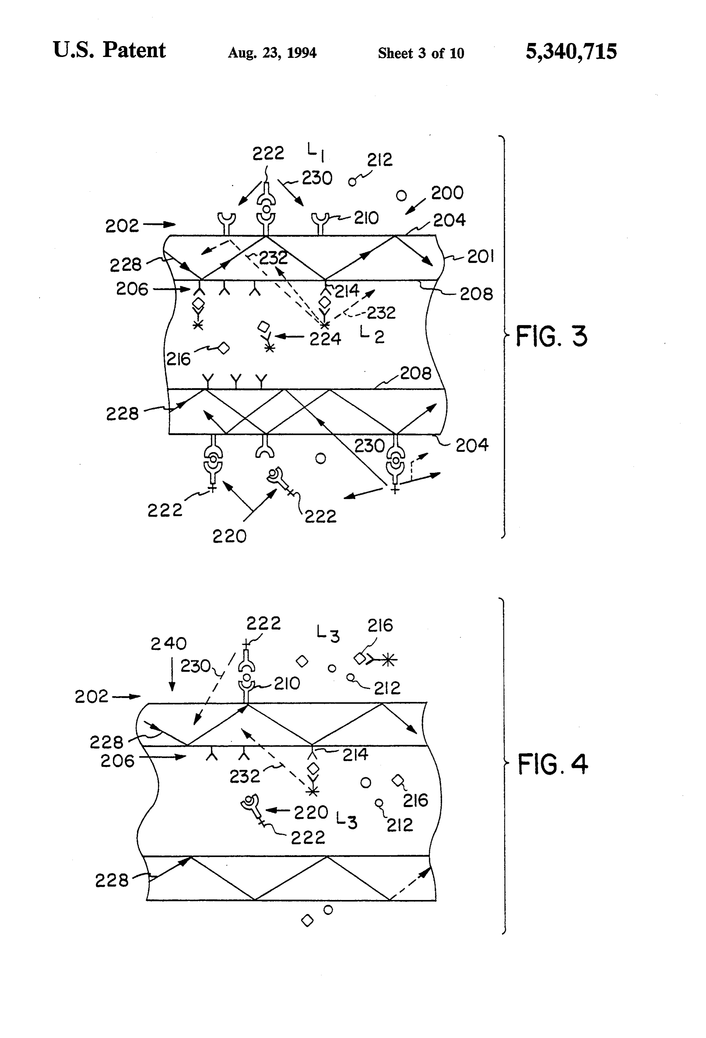
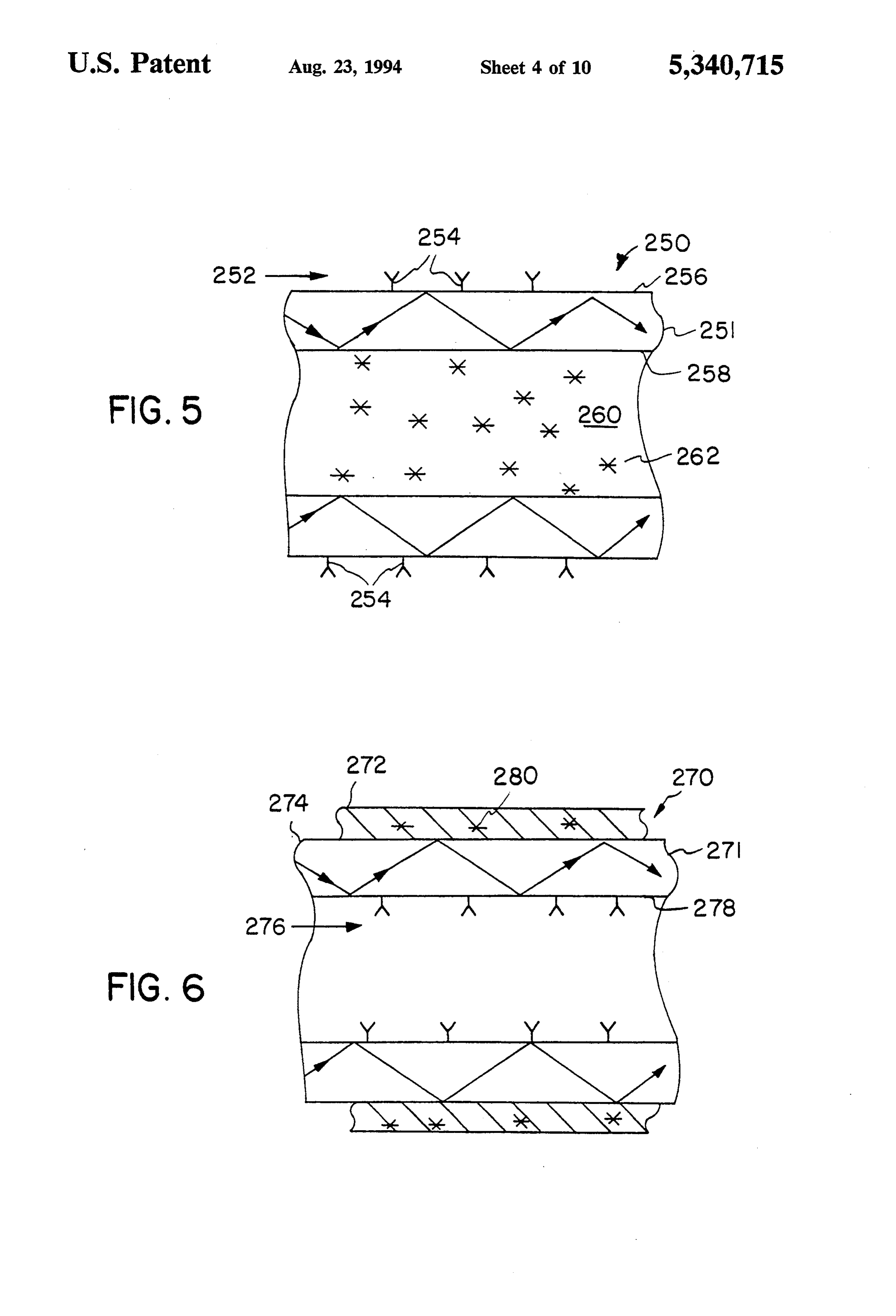
according to the invention is useful for detecting one or 10 more components of a first medium, or one or more hollow FIG. 3 is a schematic partial cross-sectional view of a components from a second medium. core having different reactant coatings 201 on This invention also features a method of assaying the inner and outer surfaces for analyzing two media; analytes by providing an optical waveguide having at hollow FIG. 4 is a schematic partial cross-sectional view of a least first and second wave propagating surfaces, and 15 lyzing acore having separate reactant coatings for ana single medium;
contacting the waveguide in the medium to contact at FIG. 5 is a schematic, partial, cross-sectional view of least one of the first and second surfaces. Radiation then a hollow core in which the inside of the rod is filled is propagated through the waveguide between the first with a gel containing a reference fluorophore; and second surfaces to generate evanescent wave elec FIG. 6 is a schematic partial cross-sectional view of a tromagnetic fields at both the first and second surfaces 20 hollow core having a solid coating covering the outer to irradiate the medium, and radiation reentering the surface and containing a reference fluorophore. Addi waveguide and emitted from it, and is detected to assay tionally, the solid coating 272 provides a handle for the analyte. The radiation can interact with an analyte manipulation of the sensor 270 without marring an opti by absorption or by generation of fluorescent radiation. cal surface;
OBJECTS OF THE INVENTION 25 FIG. 7 is a schematic partial cross-sectional view of a hollow core having a reactant coating disposed about
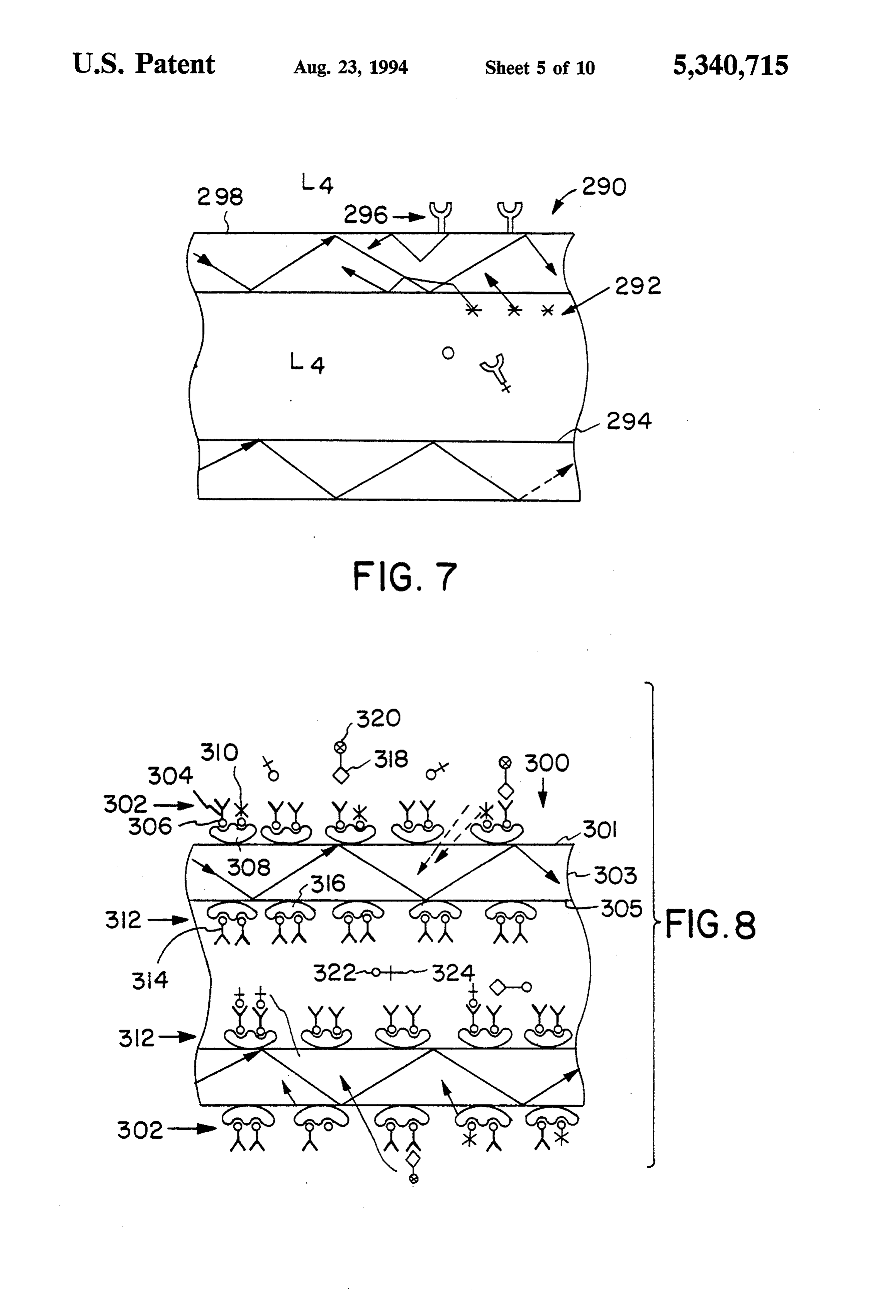
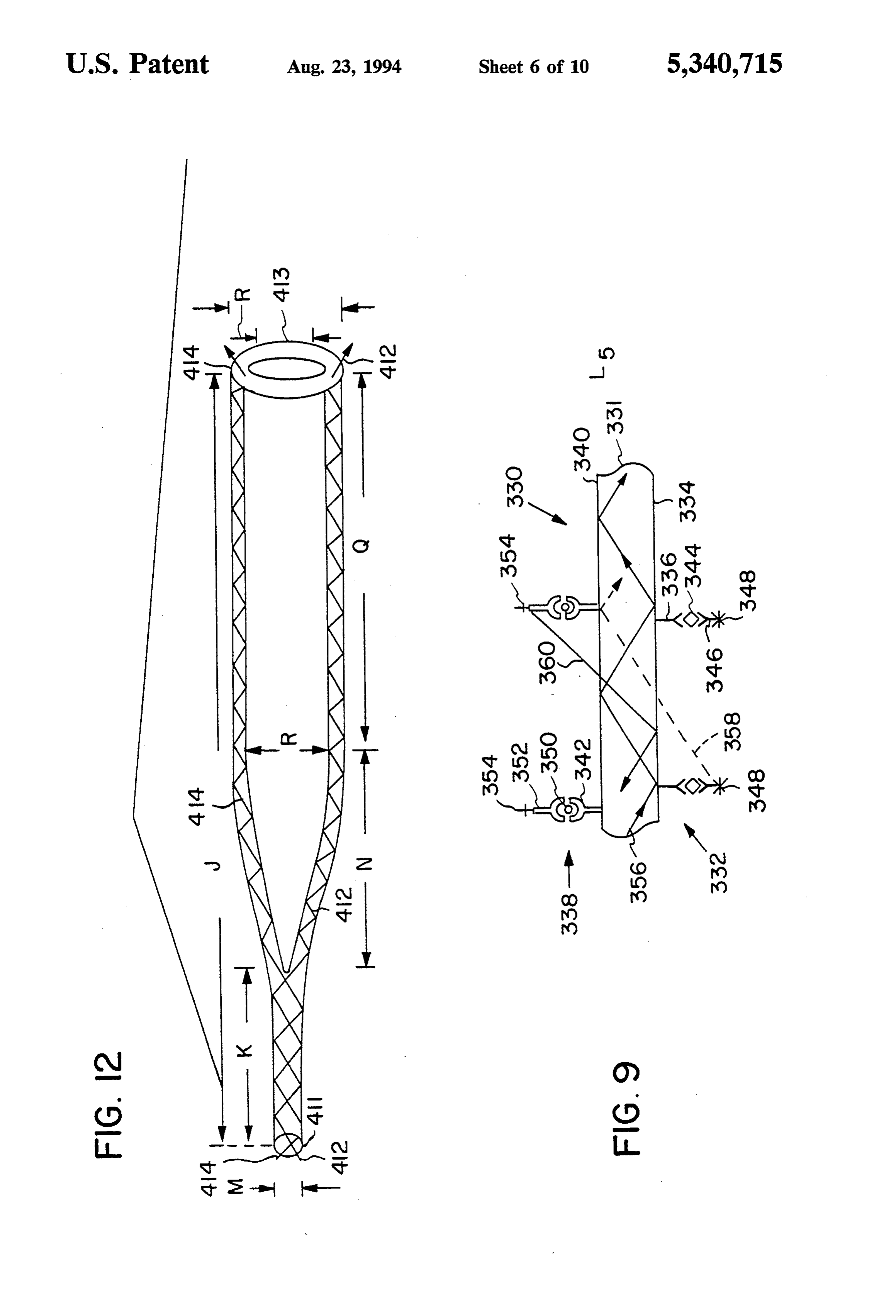
It is among the objects of the invention to provide an its outer surface and a reference fluorophore attached to improved optical waveguide sensor, apparatus, and the inner surface for analyzing a single medium; method for analyzing at least one medium and, in partic FIG. 8 is a schematic partial cross-sectional view of a ular, for conducting fluorescent immunoassays. hollow core having two surfaces coated with avidin to Another object of the invention is to provide a sensor bind a first antibody and a reference to the outer surface having at least two optically independent surfaces and a second antibody to the inner surface; which can be illuminated by one or more light input FIG. 9 is a schematic partial cross-sectional view of signals. planar waveguide having fluorophores which transfer Yet another object of the invention is to provide such 35 energy across the waveguide;
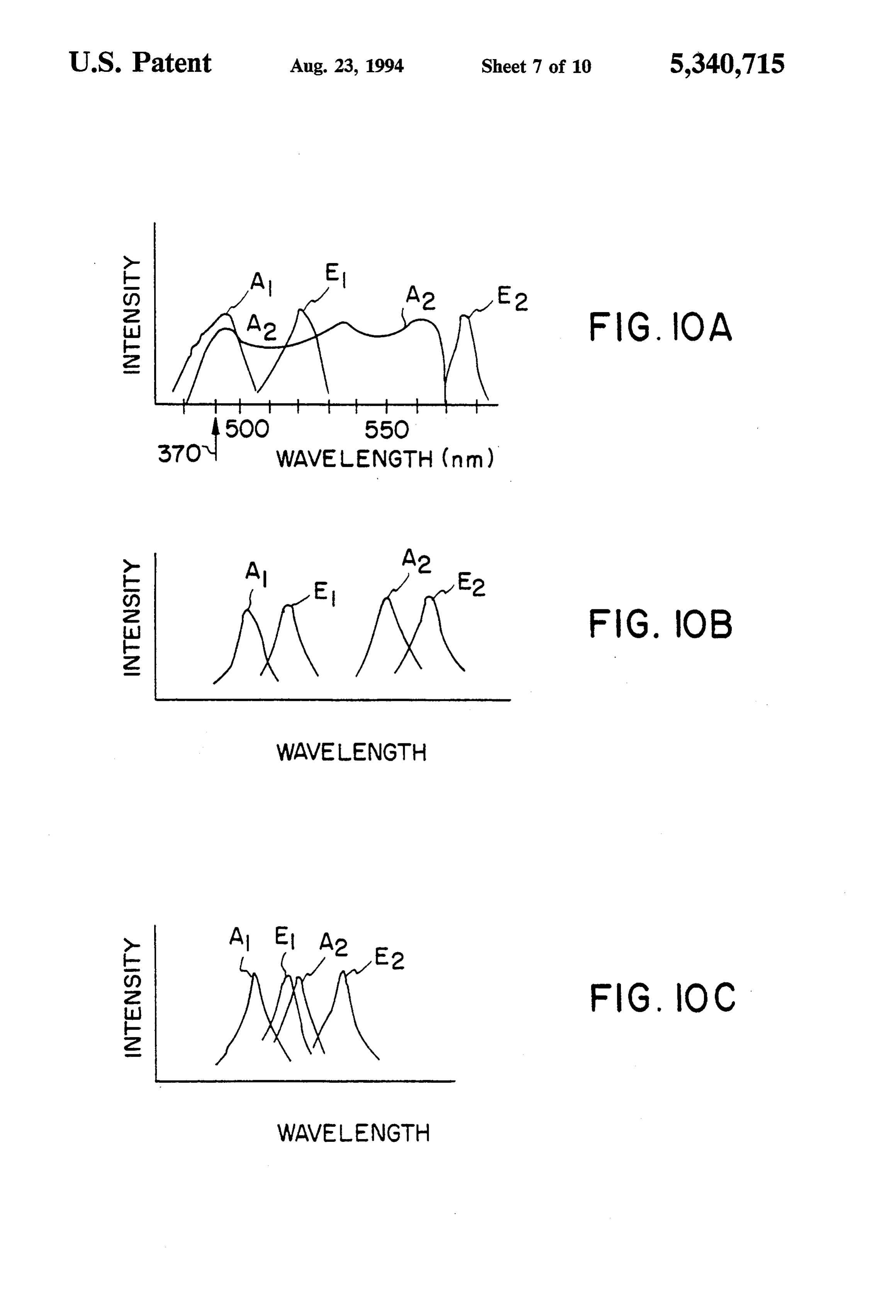
a sensor which enables two independent assays to be FIG. 10A is a chart of intensity versus wavelength conducted using a single waveguide. showing overlapping absorption or excitation wave A still further object of the invention is to provide lengths and two different emission wavelengths; such a sensor which can enable comparison of a refer FIG. 10B is a chart showing two fluorophores having ence output signal with an analyte output signal to de different absorption and emission spectra; termine fluctuations in light intensity or loss due to FIG. 10C is a chart showing overlapping spectra of surface defects. the emission wavelength of a first fluorophore and the Yet another object of the invention is to provide such absorption wavelength of a second fluorophore; a sensor which enables a greater acceptable variation of 45 FIG. 11A is a schematic partial cross-sectional view sensor geometry by providing automatic referencing of a cone used as a launcher to deliver light to an end of within the waveguide. the hollow core;
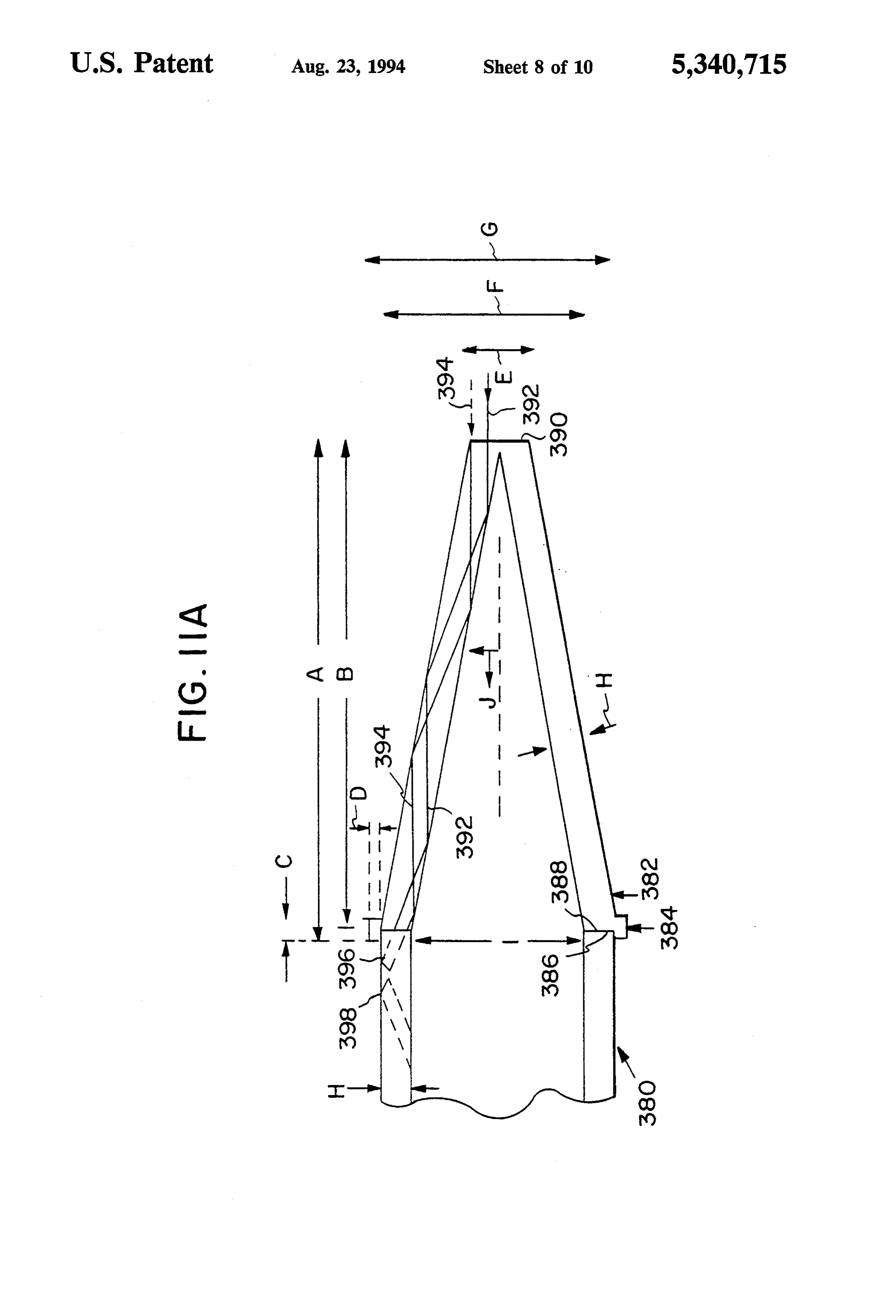
It is a further object of the invention to provide such of FIG.
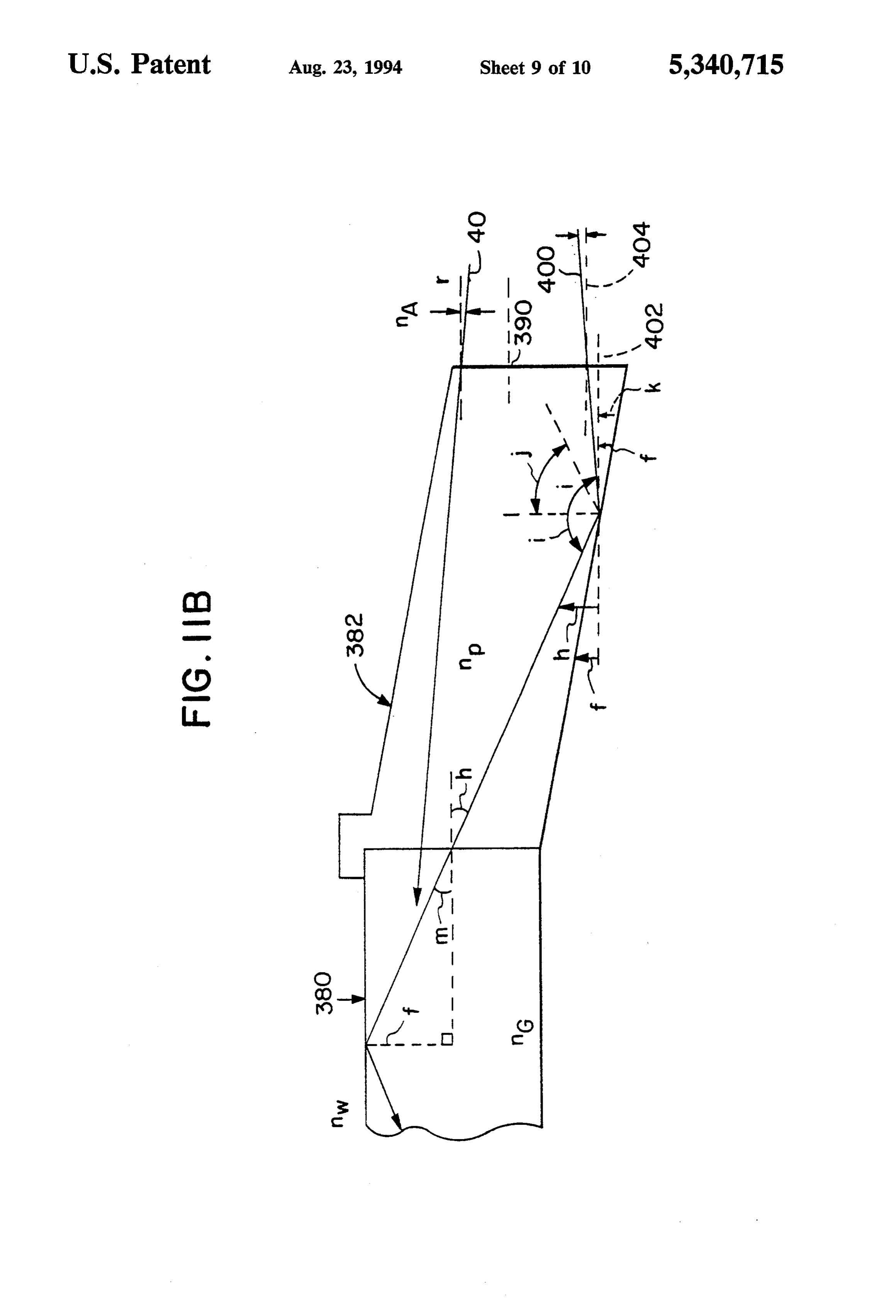
the 11B is an enlarged schematic view of a portion device of FIG. 10A illustrating the reflection of a a sensor which provides accurate output signals which propagated light ray;
are independent of a change in diameter or wall thick 50 FIG. 12 is a schematic cross-sectional view of an ness of the sensor.
Yet another object of the invention is to provide a alternative launcher for delivering light to a hollow sensor which can provide a reference of excitation radi core; and ation without contacting the sample with the reference FIG. 13 is a schematic representation of a sensing material.
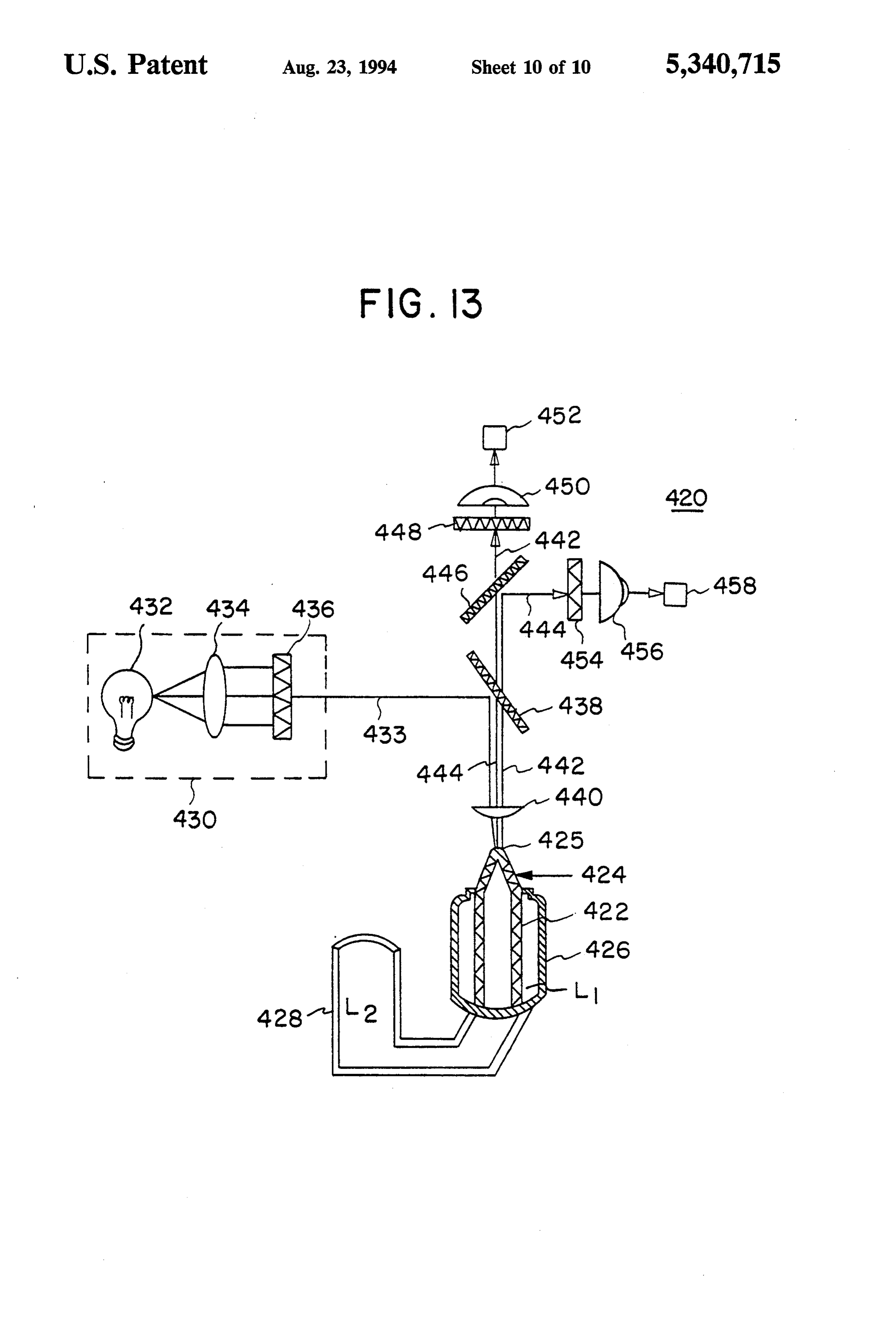
apparatus according to the invention for detecting two 55 output wavelengths.
A still further object of the invention is to provide an improved device for guiding excitation radiation into a DESCRIPTION OF THE ILLUSTRATIVE sensor according to the invention, and for collecting EMBODIMENT output radiation. A sensor according to the present invention and DESCRIPTION OF THE DRAWINGS 60 method for using the sensor can be accomplished by a waveguide having at least two wave propagating sur
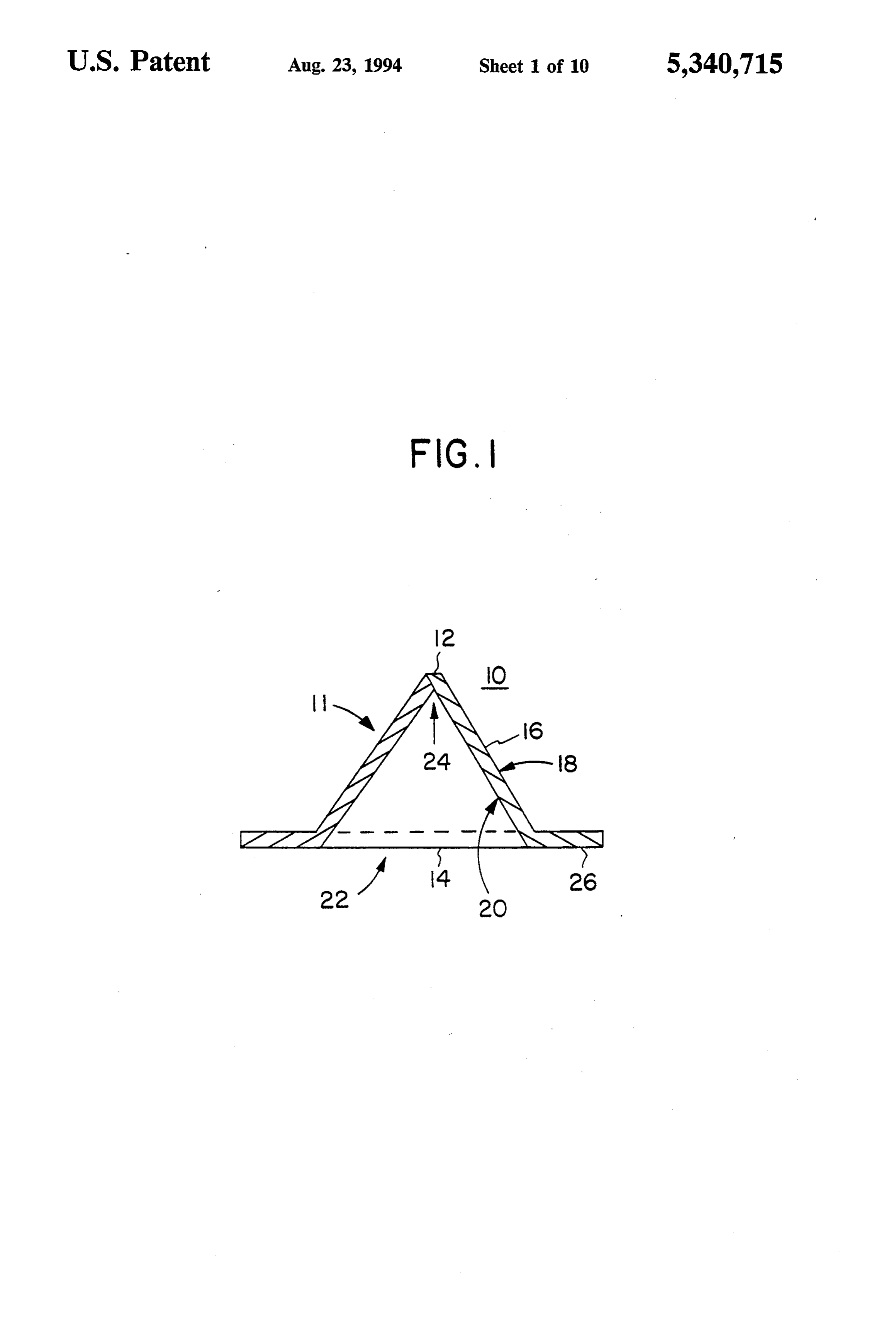
The foregoing and other objects and advantages of faces. The sensor receives a radiation input signal and the invention will be appreciated more fully from the emits one or more output signals to detect one or more following further description thereof which reference analytes in at least one medium. Analyte, as used herein, to the accompanying drawings wherein: 65 shall be understood to include any of a variety of chemi FIG. 1 is a schematic cross-sectional view of a sensor cal and biochemical substances. The analyte sources according to this invention configured as a frustoconi may include physiological, scientific and industrial cal shell; (toxic and nontoxic) test media where the presence,
Page 14
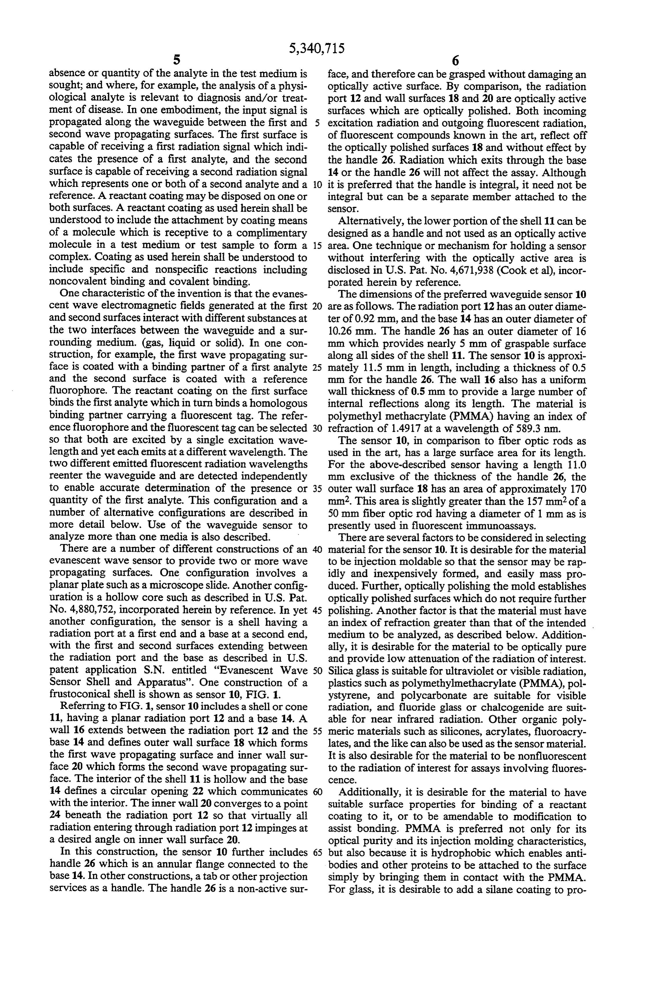
absence or quantity of the analyte in the test medium is face, and therefore can be grasped without damaging an sought; and where, for example, the analysis of a physi optically active surface. By comparison, the radiation ological analyte is relevant to diagnosis and/or treat port 12 and wall surfaces 18 and 20 are optically active ment of disease. In one embodiment, the input signal is surfaces which are optically polished. Both incoming propagated along the waveguide between the first and excitation radiation and outgoing fluorescent radiation, second wave propagating surfaces. The first surface is of fluorescent compounds known in the art, reflect off capable of receiving a first radiation signal which indi the optically polished surfaces 18 and without effect by cates the presence of a first analyte, and the second the handle 26. Radiation which exits through the base surface is capable of receiving a second radiation signal 14 or the handle 26 will not affect the assay. Although which represents one or both of a second analyte and a 10 it is preferred that the handle is integral, it need not be reference. A reactant coating may be disposed on one or integral but can be a separate member attached to the both surfaces. A reactant coating as used herein shall be SenSOT.
understood to include the attachment by coating means Alternatively, the lower portion of the shell 11 can be of a molecule which is receptive to a complimentary designed as a handle and not used as an optically active molecule in a test medium or test sample to form a 15 area. One technique or mechanism for holding a sensor complex. Coating as used herein shall be understood to without interfering with the optically active area is include specific and nonspecific reactions including disclosed in U.S. Pat. No. 4,671,938 (Cook et al), incor noncovalent binding and covalent binding. porated herein by reference.
One characteristic of the invention is that the evanes The dimensions of the preferred waveguide sensor 10 cent wave electromagnetic fields generated at the first 20 areas follows. The radiation port 12 has an outer diame and second surfaces interact with different substances at ter of 0.92 mm, and the base 14 has an outer diameter of the two interfaces between the waveguide and a sur 10.26 mm. The handle 26 has an outer diameter of 16 rounding medium. (gas, liquid or solid). In one con mm which provides nearly 5 mm of graspable surface struction, for example, the first wave propagating sur along all sides of the shell 11. The sensor 10 is approxi face is coated with a binding partner of a first analyte 25 mately 11.5 mm in length, including a thickness of 0.5 and the second surface is coated with a reference mm for the handle 26. The wall 16 also has a uniform fluorophore. The reactant coating on the first surface wall thickness of 0.5 mm to provide a large number of binds the first analyte which in turn binds a homologous internal reflections along its length. The material is binding partner carrying a fluorescent tag. The refer polymethyl methacrylate (PMMA) having an index of ence fluorophore and the fluorescent tag can be selected 30 refraction of 1.4917 at a wavelength of 589.3 nm. so that both are excited by a single excitation wave The sensor 10, in comparison to fiber optic rods as length and yet each emits at a different wavelength. The used in the art, has a large surface area for its length. two different emitted fluorescent radiation wavelengths For the above-described sensor having a length 11.0 reenter the waveguide and are detected independently mm exclusive of the thickness of the handle 26, the to enable accurate determination of the presence or 35 outer wall surface 18 has an area of approximately 170 quantity of the first analyte. This configuration and a mm2. This area is slightly greater than the 157 mm2 of a number of alternative configurations are described in 50 mm fiber optic rod having a diameter of 1 mm as is more detail below. Use of the waveguide sensor to presently used in fluorescent immunoassays. analyze more than one media is also described. There are several factors to be considered in selecting There are a number of different constructions of an material for the sensor 10. It is desirable for the material evanescent wave sensor to provide two or more wave to be injection moldable so that the sensor may be rap propagating surfaces. One configuration involves a idly and inexpensively formed, and easily mass pro planar plate such as a microscope slide. Another config duced. Further, optically polishing the mold establishes uration is a hollow core such as described in U.S. Pat. optically polished surfaces which do not require further No. 4,880,752, incorporated herein by reference. In yet 45 polishing. Another factor is that the material must have another configuration, the sensor is a shell having a an index of refraction greater than that of the intended radiation port at a first end and a base at a second end, medium to be analyzed, as described below. Addition with the first and second surfaces extending between ally, it is desirable for the material to be optically pure the radiation port and the base as described in U.S. and provide low attenuation of the radiation of interest. patent application S.N. entitled “Evanescent Wave 50 Silica glass is suitable for ultraviolet or visible radiation, Sensor Shell and Apparatus'. One construction of a plastics such as polymethylmethacrylate (PMMA), pol frustoconical shell is shown as sensor 10, FIG. 1. ystyrene, and polycarbonate are suitable for visible Referring to FIG. 1, sensor 10 includes a shell or cone radiation, and fluoride glass or chalcogenide are suit 11, having a planar radiation port 12 and a base 14. A able for near infrared radiation. Other organic poly wall 16 extends between the radiation port 12 and the 55 meric materials such as silicones, acrylates, fluoroacry base 14 and defines outer wall surface 18 which forms lates, and the like can also be used as the sensor material. the first wave propagating surface and inner wall sur It is also desirable for the material to be nonfluorescent face 20 which forms the second wave propagating sur to the radiation of interest for assays involving fluores face. The interior of the shell 11 is hollow and the base CeCe.
14 defines a circular opening 22 which communicates Additionally, it is desirable for the material to have with the interior. The inner wall 20 converges to a point suitable surface properties for binding of a reactant 24 beneath the radiation port 12 so that virtually all coating to it, or to be amendable to modification to radiation entering through radiation port 12 impinges at assist bonding. PMMA is preferred not only for its a desired angle on inner wall surface 20. optical purity and its injection molding characteristics, In this construction, the sensor 10 further includes 65 but also because it is hydrophobic which enables anti handle 26 which is an annular flange connected to the bodies and other proteins to be attached to the surface base 14. In other constructions, a tab or other projection simply by bringing them in contact with the PMMA. services as a handle. The handle 26 is a non-active sur For glass, it is desirable to add a silane coating to pro
Page 15
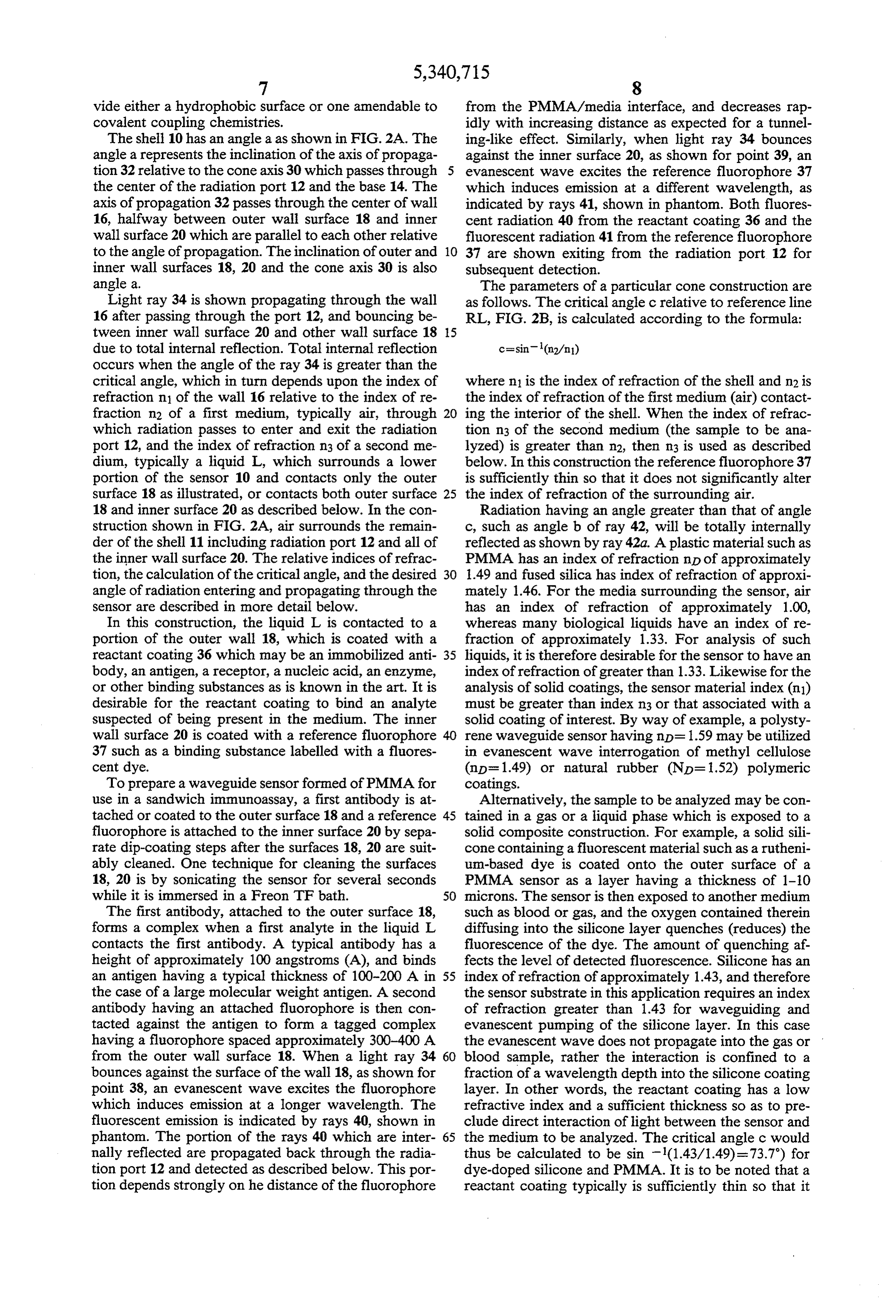
vide either a hydrophobic surface or one amendable to from the PMMA/media interface, and decreases rap covalent coupling chemistries. idly with increasing distance as expected for a tunnel The shell 10 has an angle a as shown in FIG. 2A. The ing-like effect. Similarly, when light ray 34 bounces angle a represents the inclination of the axis of propaga against the inner surface 20, as shown for point 39, an tion 32 relative to the cone axis 30 which passes through 5 evanescent wave excites the reference fluorophore 37 the center of the radiation port 12 and the base 14. The which induces emission at a different wavelength, as axis of propagation 32 passes through the center of wall indicated by rays 41, shown in phantom. Both fluores 16, halfway between outer wall surface 18 and inner cent radiation 40 from the reactant coating 36 and the wall surface 20 which are parallel to each other relative fluorescent radiation 41 from the reference fluorophore to the angle of propagation. The inclination of outer and O 37 are shown exiting from the radiation port 12 for inner wall surfaces 18, 20 and the cone axis 30 is also subsequent detection.
angle a. The parameters of a particular cone construction are Light ray 34 is shown propagating through the wall as follows. The critical angle c relative to reference line 16 after passing through the port 12, and bouncing be RL, FIG. 2B, is calculated according to the formula: tween inner wall surface 20 and other wall surface 18 15 due to total internal reflection. Total internal reflection occurs when the angle of the ray 34 is greater than the critical angle, which in turn depends upon the index of where n is the index of refraction of the shell and n2 is refraction in of the wall 16 relative to the index of re the index of refraction of the first medium (air) contact fraction n2 of a first medium, typically air, through ing the interior of the shell. When the index of refrac which radiation passes to enter and exit the radiation tion n3 of the second medium (the sample to be ana port 12, and the index of refraction n3 of a second me lyzed) is greater than n2, then n3 is used as described dium, typically a liquid L, which surrounds a lower below. In this construction the reference fluorophore 37 portion of the sensor 10 and contacts only the outer is sufficiently thin so that it does not significantly alter surface 18 as illustrated, or contacts both outer surface 25 the index of refraction of the surrounding air. 18 and inner surface 20 as described below. In the con Radiation having an angle greater than that of angle struction shown in FIG. 2A, air surrounds the remain c, such as angle b of ray 42, will be totally internally der of the shell 11 including radiation port 12 and all of reflected as shown by ray 42a. A plastic material such as the inner wall surface 20. The relative indices of refrac PMMA has an index of refraction nD of approximately tion, the calculation of the critical angle, and the desired 30 1.49 and fused silica has index of refraction of approxi angle of radiation entering and propagating through the mately 1.46. For the media surrounding the sensor, air sensor are described in more detail below. has an index of refraction of approximately 1.00, In this construction, the liquid L is contacted to a whereas many biological liquids have an index of re portion of the outer wall 18, which is coated with a fraction of approximately 1.33. For analysis of such reactant coating 36 which may be an immobilized anti 35 liquids, it is therefore desirable for the sensor to have an body, an antigen, a receptor, a nucleic acid, an enzyme, index of refraction of greater than 1.33. Likewise for the or other binding substances as is known in the art. It is analysis of solid coatings, the sensor material index (n1) desirable for the reactant coating to bind an analyte must be greater than index n3 or that associated with a suspected of being present in the medium. The inner solid coating of interest. By way of example, a polysty wall surface 20 is coated with a reference fluorophore 40 rene waveguide sensor having nD= 1.59 may be utilized 37 such as a binding substance labelled with a fluores in evanescent wave interrogation of methyl cellulose cent dye. (nD=1.49) or natural rubber (ND=1.52) polymeric To prepare a waveguide sensor formed of PMMA for coatings.
use in a sandwich immunoassay, a first antibody is at Alternatively, the sample to be analyzed may be con tached or coated to the outer surface 18 and a reference 45 tained in a gas or a liquid phase which is exposed to a fluorophore is attached to the inner surface 20 by sepa solid composite construction. For example, a solid sili rate dip-coating steps after the surfaces 18, 20 are suit cone containing a fluorescent material such as a rutheni ably cleaned. One technique for cleaning the surfaces um-based dye is coated onto the outer surface of a 18, 20 is by sonicating the sensor for several seconds PMMA sensor as a layer having a thickness of 1-10 while it is immersed in a Freon TF bath. SO microns. The sensor is then exposed to another medium The first antibody, attached to the outer surface 18, such as blood or gas, and the oxygen contained therein forms a complex when a first analyte in the liquid L. diffusing into the silicone layer quenches (reduces) the contacts the first antibody. A typical antibody has a fluorescence of the dye. The amount of quenching af. height of approximately 100 angstroms (A), and binds fects the level of detected fluorescence. Silicone has an an antigen having a typical thickness of 100-200 A in 55 index of refraction of approximately 1.43, and therefore the case of a large molecular weight antigen. A second the sensor substrate in this application requires an index antibody having an attached fluorophore is then con of refraction greater than 1.43 for waveguiding and tacted against the antigen to form a tagged complex evanescent pumping of the silicone layer. In this case having a fluorophore spaced approximately 300-400 A the evanescent wave does not propagate into the gas or from the outer wall surface 18. When a light ray 34 60 blood sample, rather the interaction is confined to a bounces against the surface of the wall 18, as shown for fraction of a wavelength depth into the silicone coating point 38, an evanescent wave excites the fluorophore layer. In other words, the reactant coating has a low which induces emission at a longer wavelength. The refractive index and a sufficient thickness so as to pre fluorescent emission is indicated by rays 40, shown in clude direct interaction of light between the sensor and phantom. The portion of the rays 40 which are inter 65 the medium to be analyzed. The critical angle c would nally reflected are propagated back through the radia thus be calculated to be sin - (1.43/1.49)=73.7) for tion port 12 and detected as described below. This por dye-doped silicone and PMMA. It is to be noted that a tion depends strongly on he distance of the fluorophore reactant coating typically is sufficiently thin so that it
Page 16
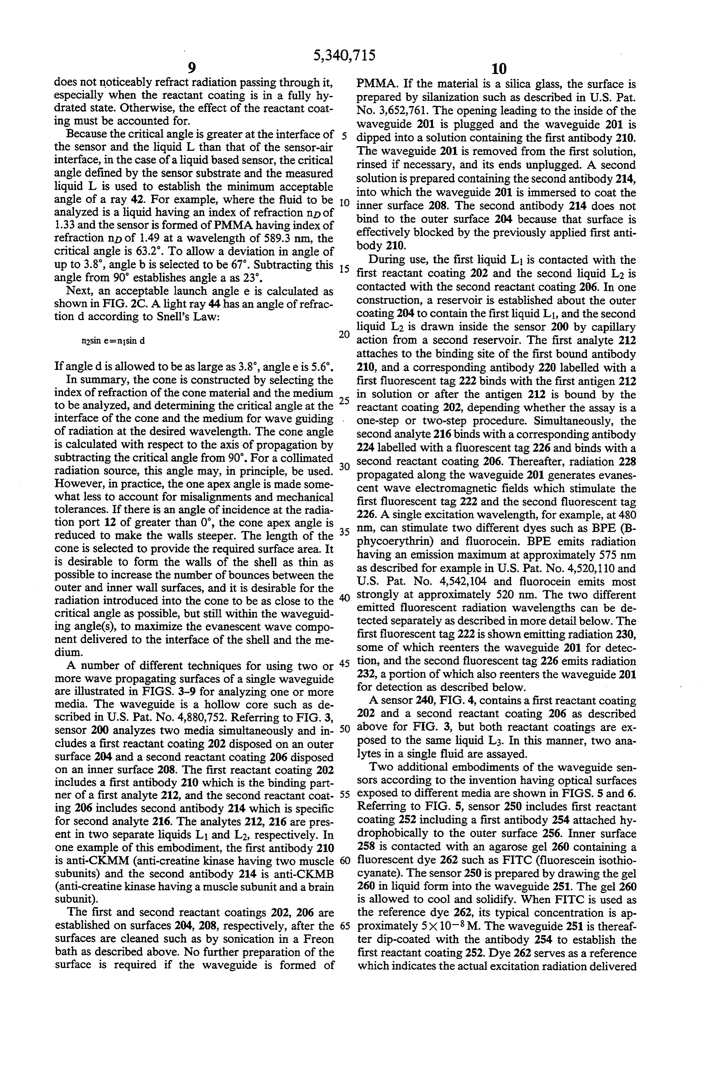
does not noticeably refract radiation passing through it, PMMA. If the material is a silica glass, the surface is especially when the reactant coating is in a fully hy prepared by silanization such as described in U.S. Pat. drated state. Otherwise, the effect of the reactant coat No. 3,652,761. The opening leading to the inside of the ing must be accounted for. waveguide 201 is plugged and the waveguide 201 is Because the critical angle is greater at the interface of 5 dipped into a solution containing the first antibody 210. the sensor and the liquid L than that of the sensor-air The waveguide 201 is removed from the first solution, interface, in the case of a liquid based sensor, the critical rinsed if necessary, and its ends unplugged. A second angle defined by the sensor substrate and the measured solution is prepared containing the second antibody 214, liquid L is used to establish the minimum acceptable into angle of a ray 42. For example, where the fluid to be 10 innerwhich the waveguide 201 is immersed to coat the surface 208. The second antibody 214 does not analyzed is a liquid having an index of refraction nD of bind to the outer 1.33 and the sensor is formed of PMMA having index of effectively blockedsurface by the 204 because that surface is previously applied first anti refraction nD of 1.49 at a wavelength of 589.3 nm, the body 210.
critical angle is 63.2. To allow a deviation in angle of up to 3.8", angle b is selected to be 67. Subtracting this 15 During use, the first liquid L1 is contacted with the angle from 90 establishes angle a as 23. first reactant coating 202 and the second liquid L2 is Next, an acceptable launch angle e is calculated as contacted with the second reactant coating 206. In one shown in FIG. 2C. A light ray 44 has an angle of refrac construction, a reservoir is established about the outer tion d according to Snell's Law: coating 204 to contain the first liquid L.1, and the second 20 liquid L2 is drawn inside the sensor 200 by capillary n2sines=nsin d action from a second reservoir. The first analyte 212 attaches to the binding site of the first bound antibody
If angle d is allowed to be as large as 3.8", angle e is 5.6. 210, and a corresponding antibody 220 labelled with a In summary, the cone is constructed by selecting the first fluorescent tag 222 binds with the first antigen 212 index of refraction of the cone material and the medium in solution or after the antigen 212 is bound by the to be analyzed, and determining the critical angle at the 25 reactant coating 202, depending whether the assay is a interface of the cone and the medium for wave guiding . one-step or two-step procedure. Simultaneously, the of radiation at the desired wavelength. The cone angle second analyte 216 binds with a corresponding antibody is calculated with respect to the axis of propagation by 224 labelled with a fluorescent tag 226 and binds with a subtracting the critical angle from 90. For a collimated 30 second reactant coating 206. Thereafter, radiation 228 radiation source, this angle may, in principle, be used. propagated along the waveguide 201 generates evanes However, in practice, the one apex angle is made some cent wave electromagnetic fields which stimulate the what less to account for misalignments and mechanical first fluorescent tag 222 and the second fluorescent tag tolerances. If there is an angle of incidence at the radia tion port 12 of greater than 0, the cone apex angle is 35 226. nm,
A single excitation wavelength, for example, at 480 can stimulate two different dyes such as BPE (Breduced to make the walls steeper. The length of the phycoerythrin) and fluorocein. BPE emits radiation cone is selected to provide the required surface area. It having an emission maximum at approximately 575 nm. is desirable to form the walls of the shell as thin as possible to increase the number of bounces between the U.S. Pat. No. 4,542,104inand as described for example U.S. Pat. No. 4,520,110 and fluorocein emits most outer and inner wall surfaces, and it is desirable for the strongly at approximately 520 nm. The two different radiation introduced into the cone to be as close to the emitted fluorescent radiation wavelengths critical angle as possible, but still within the waveguid tected separately as described in more detail below. can be de ing angle(s), to maximize the evanescent wave compo first fluorescent tag 222 is shown emitting radiation The 230, nent delivered to the interface of the shell and the me dium. some of which reenters the waveguide 201 for detec A number of different techniques for using two or 45 232, tion, and the second fluorescent tag 226 emits radiation more wave propagating surfaces of a single waveguide a portion of which also reenters the waveguide 201 are illustrated in FIGS. 3-9 for analyzing one or more for detection as described below.
media. The waveguide is a hollow core such as de A sensor 240, FIG. 4, contains a first reactant coating scribed in U.S. Pat. No. 4,880,752. Referring to FIG. 3, 202 and a second reactant coating 206 as described sensor 200 analyzes two media simultaneously and in 50 above for FIG. 3, but both reactant coatings are ex cludes a first reactant coating 202 disposed on an outer posed to the same liquid L3. In this manner, two ana surface 204 and a second reactant coating 206 disposed lytes in a single fluid are assayed.
on an inner surface 208. The first reactant coating 202 Two additional embodiments of the waveguide sen includes a first antibody 210 which is the binding part sors according to the invention having optical surfaces ner of a first analyte 212, and the second reactant coat 55 exposed to different media are shown in FIGS. 5 and 6. ing 206 includes second antibody 214 which is specific Referring to FIG. 5, sensor 250 includes first reactant for second analyte 216. The analytes 212, 216 are pres coating 252 including a first antibody 254 attached hy ent in two separate liquids L1 and L2, respectively. In drophobically to the outer surface 256. Inner surface one example of this embodiment, the first antibody 210 258 is contacted with an agarose gel 260 containing a is anti-CKMM (anti-creatine kinase having two muscle fluorescent dye 262 such as FITC (fluorescein isothio subunits) and the second antibody 214 is anti-CKMB cyanate). The sensor 250 is prepared by drawing the gel (anti-creatine kinase having a muscle subunit and a brain 260 in liquid form into the waveguide 251. The gel 260 subunit). is allowed to cool and solidify. When FITC is used as The first and second reactant coatings 202, 206 are the reference dye 262, its typical concentration is ap established on surfaces 204, 208, respectively, after the 65 proximately 5x 10⁸M. The waveguide 251 is thereaf surfaces are cleaned such as by Sonication in a Freon ter dip-coated with the antibody 254 to establish the bath as described above. No further preparation of the first reactant coating 252. Dye 262 serves as a reference surface is required if the waveguide is formed of which indicates the actual excitation radiation delivered
Page 17
to fluorescent tags bound to the first reactant coating detected at 615 nm and 520 nm, respectively. In the use 252. of two or more services according to the present inven By comparison, the sensor 270, FIG. 6, includes a tion, a third output wavelength at 576 mm can be de reference media 272 covering its outer surface 274 and tected when the second fluorescent tag 324 is BPE. carries a first reactant coating 276 on its inner surface Sensor 330, FIG. 9, illustrates energy transfer across 278. The media 272 in one embodiment is a solid coating two optical surfaces according to another embodiment formed of FEP (polytetrafluoroethylene-co-hexa of the invention to provide a correlated assay. The fluoropropylene) having an index of refraction of waveguide 331 is formed as a planar element such as a nD= 1.338. The FEP is doped with a fluorescent dye microscope slide. The first reactant coating 332 at 280 such as ruthenium (tris2,2'-bypyridiyl ruthenium II 10 tached to first surface 334 includes attached first anti dichloride) and forms a layer approximately 10 microns body 336 such as anti-CKMM, and second reactant of thickness. The FEP layer is applied to the outer coating 338 attached to second surface 340. The second surface 274 after the ends of the waveguide 271 are reactant coating 338 includes attached antibody 342 capped. The ends are then decapped and the waveguide such as anti-CKMB. In this embodiment, the attached 271 is dip-coated with the antibody 276. 15 anti-CKMM antibody 336 binds CKMM antigen 344 Sensor 290, FIG. 7, includes a reference 292 attached which in turn binds taqged anti-CKMM antibody 346 to inner surface 294 and a first reactant coating 296 having fluorophore 348 such as RPE (R-phycoeryth attached to outer surface 298. The sensor 290 is useful rin). The anti-CKMB second antibody 342 binds with a for analyzing a single medium L4 when it is not neces CKMB second antigen 350 which in turn binds anti sary to isolate the reference dye 292 from the medium 20 CKMB antibody 352 with fluorescent tag 354 such as being analyzed. Comparison, sensor 250, FIG. 5, and APC (allophycocyanin).
sensor 270, FIG. 6, isolate the reference dyes from the During use, the sensor 330 is immersed in a liquid L5 medium being analyzed. In contrast, sensor 250, FIG. 5, suspected to contain both CKMM antigen 334 and and sensor 270, FIG. 6, isolate the reference dyes from CKMB antigen 350. Blue excitation radiation 356 at the medium being analyzed. 25 approximately 485 nm is propagated between the first Sensor 300, FIG. 8, assays two analytes in a medium and second surfaces 334 and 340. Green light is emitted and simultaneously provides a reference. Additionally, at approximately 576 mm from the RPE dye 348 only both surfaces are coated with avidin to provide initial when the CKMM antigen 344 is present. The bound binding surfaces 308 and 316. The first reactant coating RPE dye 348 is excited by the evanescent wave electro 302 includes a first antibody 304 which is biotinylated, 30 magnetic fields and emits green light 358 which reenters that is, a biotin molecule 306 is attached to the antibody the waveguide 331 and produces additional evanescent 304 to enable binding with the avidin 308. The first wave effects. The effects excite the APC dye 354 which coating 302 also contains a biotinylated reference dye emits red light 360 at a wavelength of approximately 310, such as fluorescein. A second coating 312 includes 660 nm. The ratio of green to red light can be used to second antibody 314 which is biotinylated to bind with 35 determine the relevant amounts of CKMM antigen to the avidin 316. Alternative binding molecules/pairs are CKMB antigen, or simply the red wavelength 360 can well known in the art and may be utilized with the be monitored to confirm the presence of both antigens. sensors of the present invention depending in part on In an alternative embodiment, the second coating 338 is the analytes sought to be detected. a nonreactive coating containing APC. The APC dye The first antibody 304 binds with first analyte 318 will be stimulated only if CKMM antigen is present, which is labelled with a fluorescent tag 320. The second because the RPE dye 348 must be present in order the antibody 314 binds a second analyte 322 carrying a excite the APC. When a known amount of APC is used, fluorescent tag 324. In one embodiment, the first anti the ratio of green to red light provides an indication of body 304 is anti-CKMM and the second antibody 314 is the actual amount of CKMM antigen present in the anti-CKMB. The first tag 320 is Texas Red (R) and the 45 liquid L5.
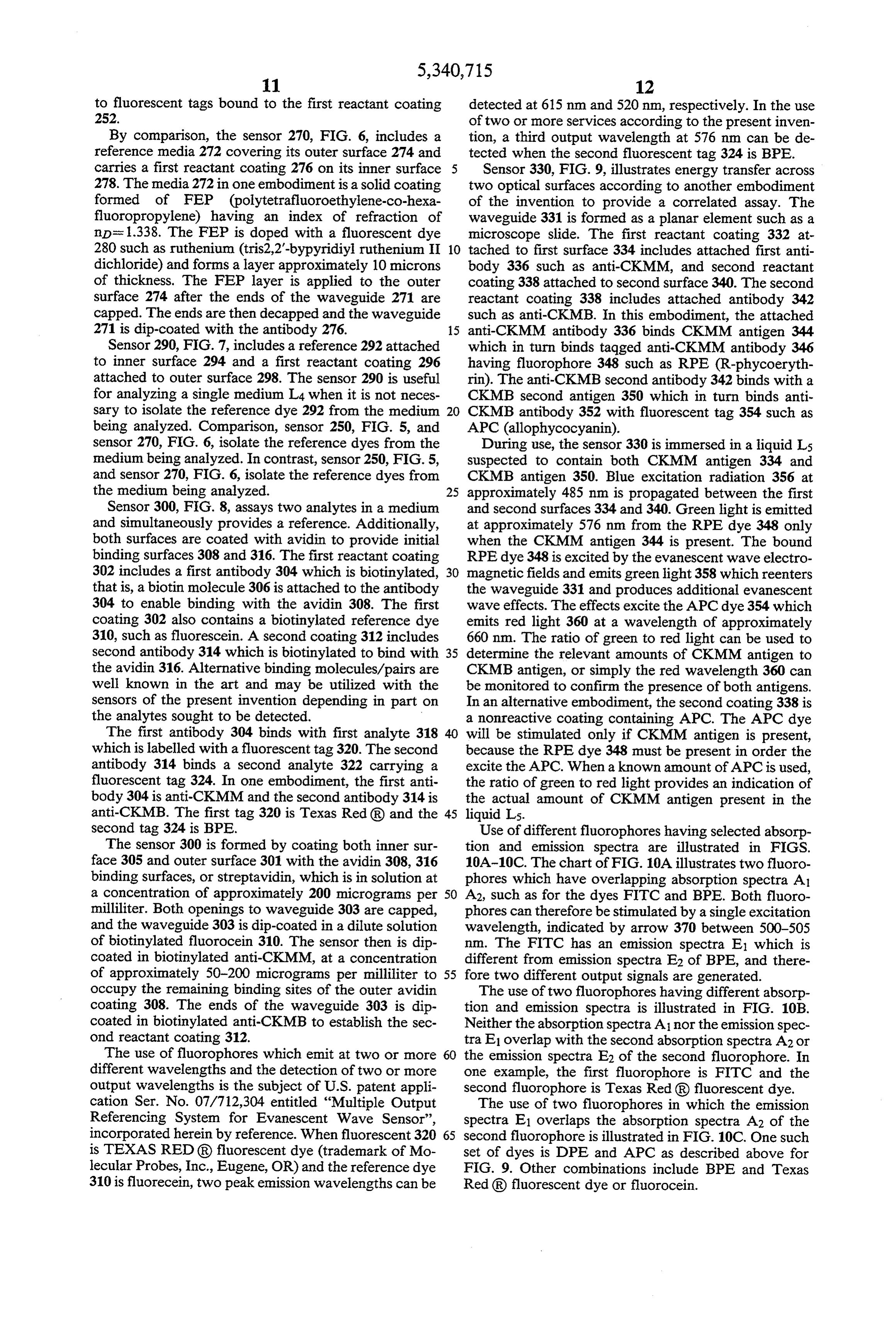
second tag 324 is BPE. Use of different fluorophores having selected absorp The sensor 300 is formed by coating both inner sur tion and emission spectra are illustrated in FIGS. face 305 and outer surface 301 with the avidin 308, 316 10A-10C. The chart of FIG. 10A illustrates two fluoro binding surfaces, or streptavidin, which is in solution at phores which have overlapping absorption spectra Al a concentration of approximately 200 micrograms per 50 A2, such as for the dyes FITC and BPE. Both fluoro milliliter. Both openings to waveguide 303 are capped, phores can therefore bestimulated by a single excitation and the waveguide 303 is dip-coated in a dilute solution wavelength, indicated by arrow 370 between 500-505 of biotinylated fluorocein 310. The sensor then is dip nm. The FITC has an emission spectra El which is coated in biotinylated anti-CKMM, at a concentration different from emission spectra E2 of BPE, and there of approximately 50-200 micrograms per milliliter to 55 fore two different output signals are generated. occupy the remaining binding sites of the outer avidin The use of two fluorophores having different absorp coating 308. The ends of the waveguide 303 is dip tion and emission spectra is illustrated in FIG. 10B. coated in biotinylated anti-CKMB to establish the sec Neither the absorption spectra A1 nor the emission spec ond reactant coating 312. tra E1 overlap with the second absorption spectra A2 or The use of fluorophores which emit at two or more 60 the emission spectra E2 of the second fluorophore. In different wavelengths and the detection of two or more one example, the first fluorophore is FITC and the output wavelengths is the subject of U.S. patent appli second fluorophore is Texas Red (R) fluorescent dye. cation Ser. No. 07/712,304 entitled “Multiple Output The use of two fluorophores in which the emission Referencing System for Evanescent Wave Sensor', spectra E1 overlaps the absorption spectra A2 of the incorporated herein by reference. When fluorescent 320 65 second fluorophore is illustrated in FIG. 10C. One such is TEXAS RED (R) fluorescent dye (trademark of Mo set of dyes is DPE and APC as described above for lecular Probes, Inc., Eugene, OR) and the reference dye FIG. 9. Other combinations include BPE and Texas 310 is fluorecein, two peak emission wavelengths can be Red (R) fluorescent dye or fluorocein.
Page 18
Therefore, it can be seen that a number of dye combi a maximum amount of the evanescent wave electromag nations can be used with the present invention in the use netic fields are generated.
of two or more optical surfaces. A partial listing of Calculation of the angles of the launcher 382 and the suitable dyes is illustrated below in TABLE I. radiation introduced into it is shown schematically in
TABLE I
APPROXIMATE EXCITATION EMISSION
(250% WAVELENGTH WAVELENGTH
Abs RANGE max
ABBR DYE
FITC Fluorescein 475-505 493 520 isothiocyanate
Fluorescein 475-505 496 520
RPE R-Phycoerythrin 480-570 495,536 576
BPE B-Phycoerythrin 500-570 546 576 rhodamine B 500-585 578 604
TR Texas Red (R) 580-610 596 615
CPC C-phycocyanin 570-640 620 650
APC Allophycocyanin 600-660 650 660
RPC R-phycocyanin 545-635 555, 618 642
RUTHENIUM Tris (2,2'-bipyridiyl) 40.490 450 610 ruthenium II dichloride
It will also be apparent from the foregoing that a sensor according to the invention can be implemented using a cone, hollow rod, a planar element, or other FIG. 11B. First, the indeces of refraction nD for the waveguide which presents two or more different opti 25 launcher 382, the sensor 380, the air or other medium cal surfaces. Further, although the monitoring of one or between the light source and the radiation port 390, and more different wavelengths of fluorescent emission the medium to be analyzed The index of refraction na of radiation is described, other effects such as absorption air is 1.0002, the index n Wfor water is 1.3333, the index can be used instead or in combination with the above. nG of the silica glass sensor 380 is 1.4584, and the index Two different devices for delivering light into a hol 30 n of the PMMA launcher 382 is 1.4917. The object of low rod are shown in FIGS. 11A-11B and FIG. 12, the design is to produce an angle q which is equal to or respectively. The hollow rod 380, FIG. 11A, is com greater than the critical angle established between the bined with a conical launcher 382 which is similar to the sensor 380 and the medium to be analyzed. The critical conical sensor described in the cross-referenced patent angle q is calculated according to the formula. application, "Evanescent Wave Sensorship and Appa 35 ratus'. The launcher 382 includes an annular flange 384 q=sin(nW/ng) 1. which press-fits around the outside of the rod 380 to butt-couple the edge 386 of the rod 380 with the edge In this example, the critical angle q is calculated to be 388 of the launcher 382. If more secure attachment is 66.095. The entrance angle m is determined by sub desired, a nonfluorescent epoxy may be used to join tracting the angle q from 90 and in this example is surfaces 386, 388 such as Epo-Tek (R) 301 epoxy avail 23.904. Similarly, the critical angle j for the launcher able from Epoxy Technology, Inc., Billerica, Massa 382 is calculated according to equation number 1 to be chusetts. The Epo-Tek (R)301 epoxy is acceptable when 42.106. The actual angle of incidence i of the light ray the launcher 382 is formed of PMMA and the rod 380 is 400 must therefore be greater than or equal to 42.106. formed of silica glass. 45 The incident angle h is calculated according to Snell's Acceptable dimensions of the launcher 382 are as Law:
follows when the rod 380 has an inner diameter I of 1.5 mm, an outer diameter F of 2.0 mm, and a wall thickness nsin h=ngsin m 2 Hof 0.25 mm. The launcher 282 has an overall length. A of 4.45 mm and an effective length B of 4.25 mm. The 50 InThe this example, the incident angle h equals 23.338.
cone angle f is determined by identities:
overall length. A includes length C of 0.2 mm for the flange 384. The thickness D of the flange 384 is 0.1 mm. hi-f-i-90 3 Therefore, the launcher 382 has an overall diameter G of 2.2 mm and an effective diameter F of 2.0 mm. The and radiation port 390 has a diameter E of 0.5 mm. Al 55 though the radiation port 390 is shown as planar, a i-k-f=90 4. convex or concave surface may instead be used to focus or defocus incoming radiation, respectively. The therefore launcher 382 has a cone angle fof 10. The launcher 382 has a thickness H of 0.25 mm, the same as that of the 60 hollow rod 380.
The path of light rays introduced at different posi In this example, angles f and k are measured relative tions on the radiation port 390 is illustrated by rays 392, to reference line 402 which is perpendicular to the radi 394. The ray 392 is first reflected from the outer surface ation port 390. The incoming light angle 1 is measured of the hollow rod 380 at location 396 and the ray 394 is 65 relative to the reference line 404 which is also perpen first reflected at location 398, thereby generating eva dicular to the radiation port 390. nescent wave electromagnetic fields. It is desirable to For light approaching the radiation port 390 at an generate as many internal reflections as possible so that angle 1 equals 0, angle k equals 0, and angle fis less than
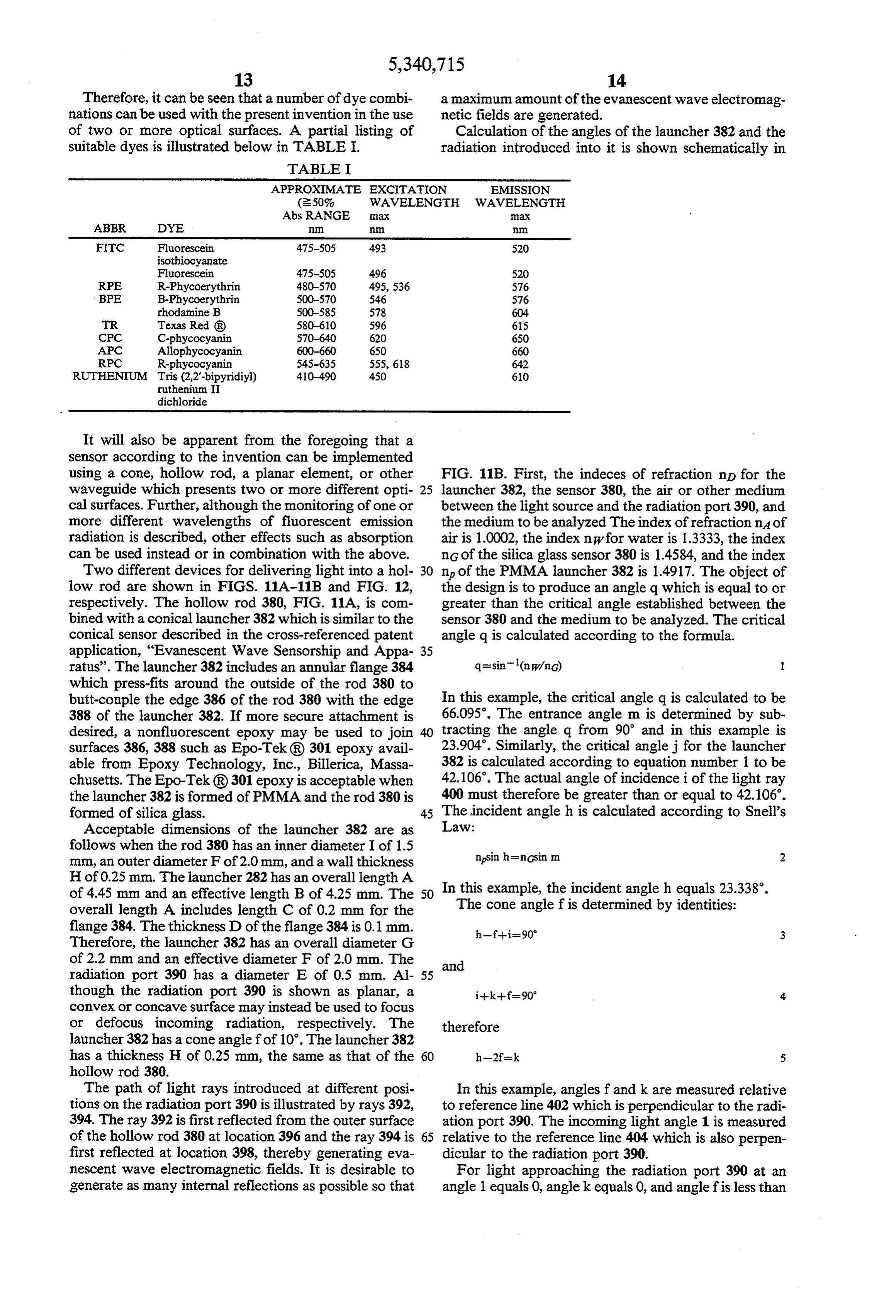
Page 19
or equal to angleh. Angle fin this example is therefore first output wavelength 442 passes through interference less than or equal to 11.669. filter 448 which blocks wavelengths other than those of If the launcher angle fis selected to be 10, then angle interest. The radiation is focused by lens 450 upon first k is 3.338. Angle 1 is calculated according to the for detector 452 which converts the first radiation output mula:
signal 442 to an electronic signal. Similarly, the second nAsin 1=nsink 6 output radiation 444 passes through an interference filter 454 and focusing lens 456, whereupon it impinges
For the above values, the incident angle 1 is 4.981 and upon second detector 458 which produces a second angle i is determined according to equation number 3 to 10 electronic output signal. The actual excitation and emis be 76.662. sion wavelengths are selected as described above for The cone angle f directly effects the incident angle 1. FIGS. 3-10C.
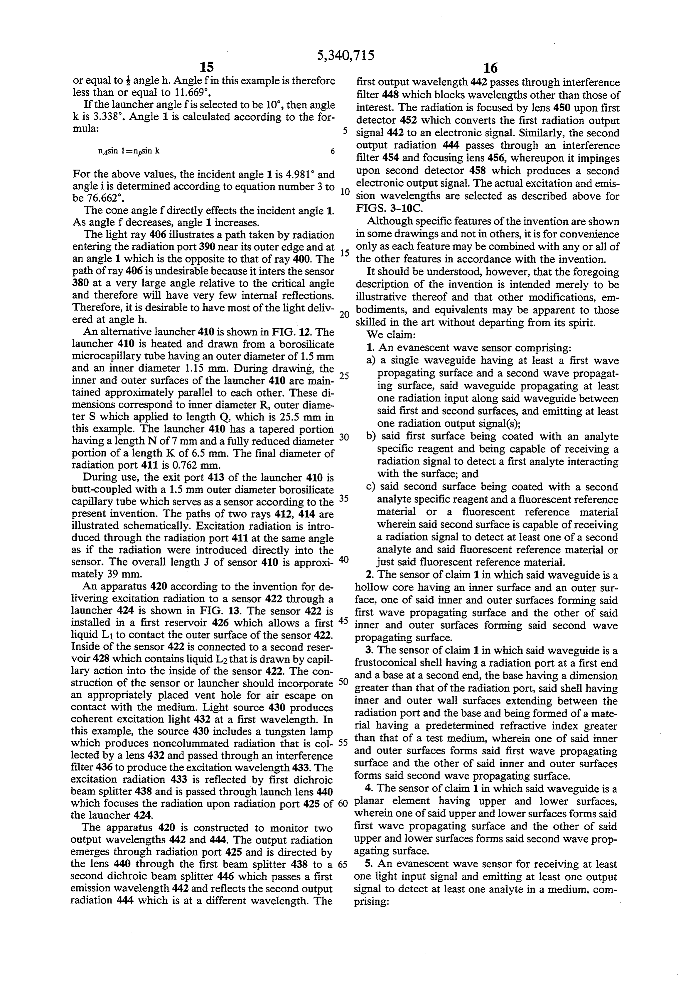
As angle f decreases, angle 1 increases. Although specific features of the invention are shown The light ray 406 illustrates a path taken by radiation in some drawings and not in others, it is for convenience entering the radiation port 390 near its outer edge and at only as each feature may be combined with any or all of an angle 1 which is the opposite to that of ray 400. The 15 the other features in accordance with the invention. path of ray 406 is undesirable because it inters the sensor It should be understood, however, that the foregoing 380 at a very large angle relative to the critical angle description of the invention is intended merely to be and therefore will have very few internal reflections. illustrative thereof and that other modifications, en Therefore, it is desirable to have most of the light deliv bodiments, and equivalents may be apparent to those ered at angle h. skilled in the art without departing from its spirit. An alternative launcher 410 is shown in FIG. 12. The We cairn:
launcher 410 is heated and drawn from a borosilicate 1. An evanescent wave sensor comprising: microcapillary tube having an outer diameter of 1.5 mm a) a single waveguide having at least a first wave and an inner diameter 1.15 mm. During drawing, the propagating surface and a second wave propagat inner and outer surfaces of the launcher 410 are main 25 ing surface, said waveguide propagating at least tained approximately parallel to each other. These di one radiation input along said waveguide between mensions correspond to inner diameter R, outer diame said first and second surfaces, and emitting at least ter S which applied to length Q, which is 25.5 mm in this example. The launcher 410 has a tapered portion 30 b) one radiation output signal(s); said first surface being coated with an analyte having a length N of 7 mm and a fully reduced diameter specific reagent and being capable of receiving a portion of a length K of 6.5 mm. The final diameter of radiation signal to detect a first analyte interacting radiation port 411 is 0.762 mm.
During use, the exit port 413 of the launcher 410 is with the surface; and butt-coupled with a 1.5 mm outer diameter borosilicate 35 c) said second surface being coated with a second capillary tube which serves as a sensor according to the analyte specific reagent and a fluorescent reference present invention. The paths of two rays 412, 414 are material or a fluorescent reference material illustrated schematically. Excitation radiation is intro wherein said second surface is capable of receiving duced through the radiation port 411 at the same angle a radiation signal to detect at least one of a second as if the radiation were introduced directly into the analyte and said fluorescent reference material or sensor. The overall length J of sensor 410 is approxi just said fluorescent reference material. mately 39 mm. 2. The sensor of claim 1 in which said waveguide is a An apparatus 420 according to the invention for de hollow core having an inner surface and an outer sur livering excitation radiation to a sensor 422 through a face, one of said inner and outer surfaces forming said launcher 424 is shown in FIG. 13. The sensor 422 is first wave propagating surface and the other of said installed in a first reservoir 426 which allows a first 45 inner and outer surfaces forming said second wave liquid L1 to contact the outer surface of the sensor 422. propagating surface.
Inside of the sensor 422 is connected to a second reser 3. The sensor of claim 1 in which said waveguide is a voir 428 which contains liquid L2 that is drawn by capil frustoconical shell having a radiation port at a first end lary action into the inside of the sensor 422. The con and a base at a second end, the base having a dimension struction of the sensor or launcher should incorporate 50 greater than that of the radiation port, said shell having an appropriately placed vent hole for air escape on inner and outer wall surfaces extending between the contact with the medium. Light source 430 produces radiation port and the base and being formed of a mate coherent excitation light 432 at a first wavelength. In this example, the source 430 includes a tungsten lamp rial having a predetermined refractive index greater than that of a test medium, wherein one of said inner which produces noncolummated radiation that is col 55 and outer surfaces forms said first wave propagating lected by a lens 432 and passed through an interference surface and the other of said inner and outer surfaces filter 436 to produce the excitation wavelength 433. The excitation radiation 433 is reflected by first dichroic forms said second wave propagating surface. beam splitter 438 and is passed through launch lens 440 4. The sensor of claim 1 in which said waveguide is a which focuses the radiation upon radiation port 425 of 60 planar element having upper and lower surfaces, the launcher 424. wherein one of said upper and lower surfaces forms said The apparatus 420 is constructed to monitor two first wave propagating surface and the other of said output wavelengths 442 and 444. The output radiation upper and lower surfaces forms said second wave prop emerges through radiation port 425 and is directed by agating surface.
the lens 440 through the first beam splitter 438 to a 65 5. An evanescent wave sensor for receiving at least second dichroic beam splitter 446 which passes a first one light input signal and emitting at least one output emission wavelength 442 and reflects the second output signal to detect at least one analyte in a medium, com radiation 444 which is at a different wavelength. The prising:
Page 20
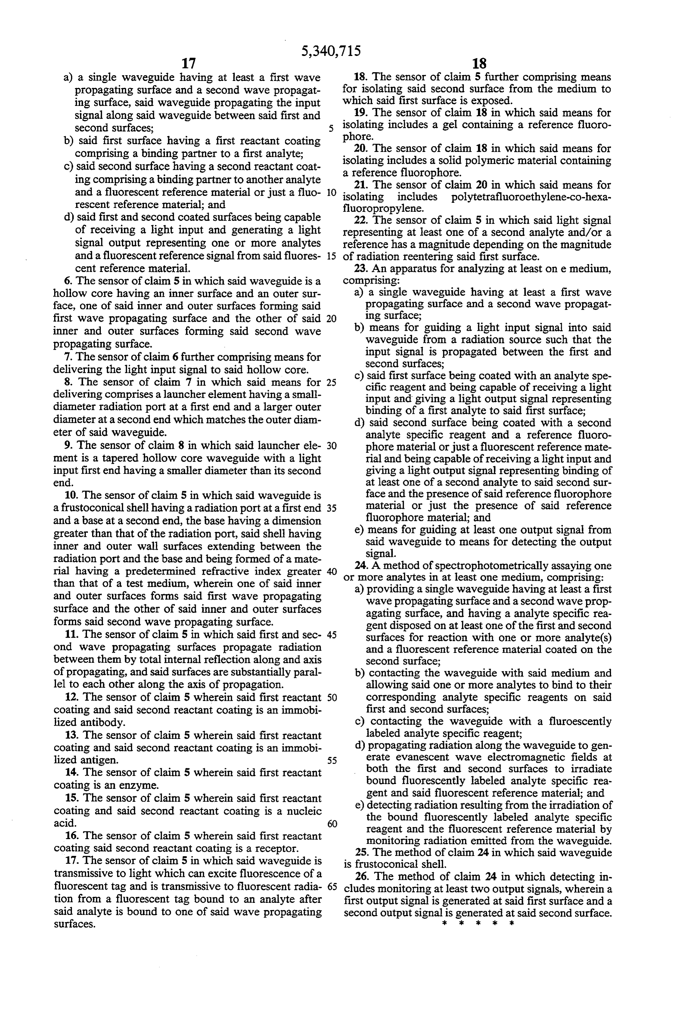
a) a single waveguide having at least a first wave 18. The sensor of claim 5 further comprising means propagating surface and a second wave propagat for isolating said second surface from the medium to ing surface, said waveguide propagating the input which said first surface is exposed. signal along said waveguide between said first and 19. The sensor of claim 18 in which said means for second surfaces; isolating includes a gel containing a reference fluoro b) said first surface having a first reactant coating phore.
comprising a binding partner to a first analyte; 20. The sensor of claim 18 in which said means for isolating c) said second surface having a second reactant coat a reference includes a solid polymeric material containing ing comprising a binding partner to another analyte fluorophore.
21. The sensor of claim 20 in which said means for and a fluorescent reference material or just a fluo O isolating includes polytetrafluoroethylene-co-hexa rescent reference material; and fluoropropylene.
d) said first and second coated surfaces being capable 22. The sensor of claim 5 in which said light signal of receiving a light input and generating a light representing at least one of a second analyte and/or a signal output representing one or more analytes reference has a magnitude depending on the magnitude and a fluorescentreference signal from said fluores 15 of radiation reentering said first surface. cent reference material. 23. An apparatus for analyzing at least one medium, 6. The sensor of claim 5 in which said waveguide is a comprising:
hollow core having an inner surface and an outer sur a) a single waveguide having at least a first wave face, one of said inner and outer surfaces forming said propagating surface and a second wave propagat first wave propagating surface and the other of said 20 ing surface;
inner and outer surfaces forming said second wave b) means for guiding a light input signal into said propagating surface. waveguide from a radiation source such that the 7. The sensor of claim 6 further comprising means for input signal is propagated between the first and delivering the light input signal to said hollow core. second surfaces;
8. The sensor of claim 7 in which said means for 25 c) cific said first surface being coated with an analyte spe reagent and being capable of receiving a light delivering comprises a launcher element having a small input and giving a light output signal representing diameter radiation port at a first end and a larger outer binding of a first analyte to said first surface; diameter at a second end which matches the outer diam d) said second surface being coated with a second eter of said waveguide. analyte specific reagent and a reference fluoro 9. The sensor of claim 8 in which said launcher ele 30 phore material or just a fluorescent reference mate ment is a tapered hollow core waveguide with a light rial and being capable of receiving a light input and input first end having a smaller diameter than its second giving a light output signal representing binding of end. at least one of a second analyte to said second sur 10. The sensor of claim 5 in which said waveguide is face and the presence of said reference fluorophore a frustoconical shell having a radiation port at a first end 35 material or just the presence of said reference and a base at a second end, the base having a dimension fluorophore material; and greater than that of the radiation port, said shell having e) means for guiding at least one output signal from inner and outer wall surfaces extending between the said waveguide to means for detecting the output radiation port and the base and being formed of a mate signal.
rial having a predetermined refractive index greater or24. A method of spectrophotometrically assaying one more analytes in at least one medium, comprising:
than that of a test medium, wherein one of said inner a) providing a single waveguide having at least a first and outer surfaces forms said first wave propagating wave propagating surface and a second wave prop surface and the other of said inner and outer surfaces agating surface, and having a analyte specific rea forms said second wave propagating surface. gent disposed on at least one of the first and second 11. The sensor of claim 5 in which said first and sec 45 surfaces for reaction with one or more analyte(s) ond wave propagating surfaces propagate radiation and a fluorescent reference material coated on the between them by total internal reflection along and axis second surface;
of propagating, and said surfaces are substantially paral b) contacting the waveguide with said medium and lel to each other along the axis of propagation. allowing said one or more analytes to bind to their 12. The sensor of claim 5 wherein said first reactant 50 corresponding analyte specific reagents on said coating and said second reactant coating is an immobi first and second surfaces; lized antibody. c) contacting the waveguide with a fluroescently 13. The sensor of claim 5 wherein said first reactant labeled analyte specific reagent; coating and said second reactant coating is an immobi d) propagating radiation along the waveguide to gen lized antigen. 55 erate evanescent wave electromagnetic fields at 14. The sensor of claim 5 wherein said first reactant both the first and second surfaces to irradiate coating is an enzyme. bound fluorescently labeled analyte specific rea 15. The sensor of claim 5 wherein said first reactant gent and said fluorescent reference material; and coating and said second reactant coating is a nucleic e) detecting radiation resulting from the irradiation of acid. 60 the bound fluorescently labeled analyte specific 16. The sensor of claim 5 wherein said first reactant reagent and the fluorescent reference material by coating said second reactant coating is a receptor. monitoring radiation emitted from the waveguide. 25. The method 17. The sensor of claim 5 in which said waveguide is is frustoconical shell. of claim 24 in which said waveguide transmissive to light which can excite fluorescence of a 26. The method of claim 24 in which detecting in fluorescent tag and is transmissive to fluorescent radia 65 cludes monitoring at least two output signals, wherein a tion from a fluorescent tag bound to an analyte after first output signal is generated at said first surface and a said analyte is bound to one of said wave propagating second output signal is: generated at: said second surface. surfaces. 3 e
Provenance
- Collection
- Cited prior art
- Original PDF
- patentimages.storage.googleapis.com →
- Filed
- 1991-06-07
- Pages
- 20
- Method
- pdftotext (the PDF's own text layer) + pdftoppm 300dpi page scans
- Source
- Google Patents bibliographic record
- Granted
- 1994-08-23
- Inventors
- Rudolf E. Slovacek; Walter F. Love; Thomas A. Cook; Richard L. Schulkind; Irene M. Walczak; Ciba Corning Diagnosys Corp
- Transcribed from
- patentimages.storage.googleapis.com →