patent · US5270636
Regulating control circuit for photovoltaic source employing switches, energy storage, and pulse width modulation controller
14 December 1993
Page 1 — bibliographic record
United States Patent (19) 11 Patent Number: 5,270,636 Lafferty (45) Date of Patent: Dec. 14, 1993
54 REGULATING CONTROL CIRCUIT FOR
PHOTOVOLTAC SOURCE EMPLOYNG FOREIGN PATENT DOCUMENTS
SWITCHES, ENERGY STORAGE, AND 2497421 7/1982 France ................................ 323/222 PULSE WOTH MODULATION 0.444172 5/1985 U.S.S.R. .............................. 323/222 CONTROLLER oTHER PUBLICATIONS 76) Inventor: Donald L. Lafferty, 724 Tampico, "Reducing Switching Stress in High Power, High Volt Walnut Creek, Calif. 94598 age DC-DC Converters' by K. Stuart, Proceedings of
21 Appl. No.: 837,328 Dunlop, J. et al., "Performance of Battery Charge Con trollers: First Year Test Report", Proc. 22nd IEEE PV 22 Filed: Feb. 18, 1992 Conf, Las Vegas, Nev., 640 (1991). 51) Int. Cl.......................... H027/00 G05F 1/613 Primary Examiner-Steven L. Stephan 52 U.S. C. ...................................... 3/33/2. Assistant Examiner-Thomas M. Dougherty 323/299; 323/906 (57) ABSTRACT (58) Field of Search ............... 323/222, 223, 299, 351, A regulating circuit controls current flow from a photo 323/906; 320/62; 136/292, 293 voltaic power source (20) to a storage battery (38) to 56 improve the conversion of solar energy to electric en (56) References Cited ergy. Two transistors (22,30) are switched on and off at
3,384,806 5/1968 Hartman ................................. 322/2 the battery. A pulse-width-modulator control chip (42) 3,696,286 10/1972 Ule ........................................ 323/15 varies the on-time of each transistor independently to 4,323,845 4/1982 Leach .................................. 323A224 provide separate control of source voltage and circuit 4,347,474 8/1982 Brooks et al. ....................... 323/224 output voltage. The source is regulated to produce 4,604,567 8/1986 Chetty .............. ... 323/299 maximum power and the output voltage is regulated to 4,725,768 2/1988 Watanabe ............................ 223 provide an optimum battery charging voltage. The E. 33 Ber a - a : maximum available energy is transferred from the 28,340 16/1989 affery. ... source to the battery, thereby improving the conversion 4,958,121 9/1990 Cuomo et al. ...................... 33/2, efficiency of the system.
5,027,051 6/1991 Lafferty .............................. 323/222 17 Claims, 1 Drawing Sheet
N 26 34
2O 38
LOAD
(BATTERY)
BASE DRIVE
CIRCUITS
DUAL PULSE.-WOTH
MODULATOR
Page 2
Drawing sheet — no readable text.
Page 3
ments of the battery while delivering maximum energy
REGULATING CONTROL CRCUT FOR to the battery.
PHOTOVOLTAC SOURCE EMPLOYNG Therefore, the present invention offers several advan SWITCHES, ENERGY STORAGE, AND PULSE tages over previous charge-control circuits. WDTH MODULATION CONTROLLER 5 Also, my circuit is simple, economical, and uses com ponents and techniques developed for highly-efficient
BACKGROUND -FIELD OF INVENTION switching power supplies.
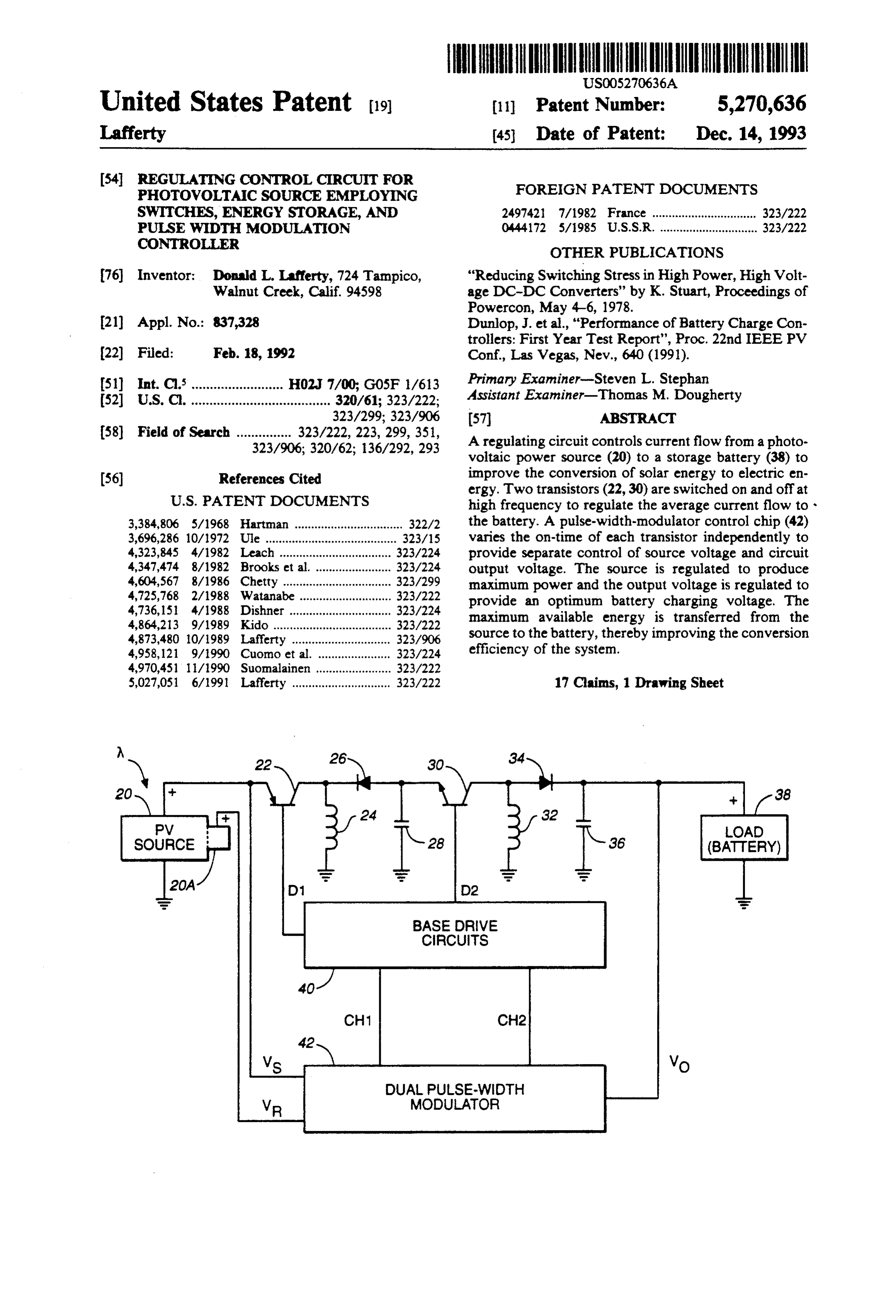
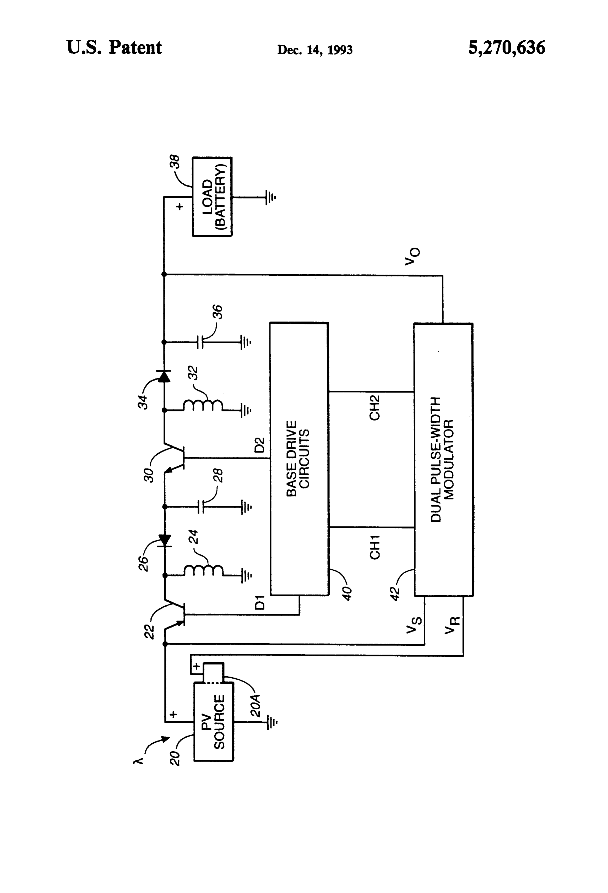
This invention relates to a system for converting solar Further objects and advantages will become apparent energy to electrical energy by an array of photovoltaic 10 as the description proceeds. cells, specifically to a circuit for improving the conver DRAWING FIGURE sion efficiency of such a system. The single drawing FIGURE shows a functional BACKGROUND - DISCUSSION OF PRIOR ART block diagram of a solar energy charge-control system which incorporates a converter with a regulated output
Photovoltaic (PV) power sources are known and 15 voltage in accordance with my invention. used for converting incident solar energy to electrical energy; such sources comprise an array of semiconduc DRAWING REFERENCE NUMERALS tor PV cells. A charge-control circuit is usually pro 20: PV power source vided to regulate current flow from the PV power 20A: PV reference cell sources to storage batteries, which store the energy. 20 22: pnp transistor, #D45 (General Electric) Ideally, such a charge-control circuit should provide a 24: 280 uh inductor voltage-current profile which conforms to the charging 26: Schottky diode characteristics of the batteries. I.e., the circuit should 8: 100 ur capacitor transfer the maximum available energy from the PV 30: npn transistor, #D44 (General Electric) source to charge the batteries. In practice, known 25 32: 280 uh inductor charge-control circuits perform these functions with 34: Schottky diode limited success, resulting in inefficient use of the energy 36: 100 uf capacitor converted by the source. 38: storage battery; 12 V, 100 amp-hours A number of circuits in current use by manufacturers 40: IC power driver chip, # TPIC2406 (Texas Instru were evaluated recently under a government-sponsored 30 ments) program established to improve reliability and perfor 42: IC control chip, # TL1451 (Texas Instruments) mance of PV power systems. Preliminary results are DESCRIPTION OF CHARGE-CONTROL presented in a recent report; Dunlop, J., et al., "Perfor CIRCUIT mance of Battery Charge Controllers: First Year Test 35
Report", Proc. of the 22nd IEEE PV Specialists Conf, The drawing FIGURE shows a schematic and block Las Vegas, Nev., 640, (1991). diagram of an electrical system, circuit, or network These reports summarize characteristics of the vari which couples a PV (photovoltaic) module (array of ous circuits and describe methods used to regulate cur PV cells) 20 to a storage battery 38. PV module 20 rent flow to the batteries. The only control exercised contains a well-known array of solar cells which con verts received solar energy to electrical energy through during the charging cycle resulted from switching off 40 the photovoltaic effect. This energy is transferred by the charging current to prevent damage to the battery. the circuit
None of the circuits could supply the full available in chemicalshown form.
to battery 38, which stores the energy
Module 20 can be of any size, type, energy to the battery.
Switching voltage regulators have been used in a 45 and number of cells, but in one preferred embodiment it number of different circuits to control power flow from contained which can 36 segments of single-crystal silicon cells maintain a 12-volt battery in a state of a photovoltaic (PV) source to a load. Some pertinent charge, provides a nominal power of 55 W at 16.8 V and examples are illustrated in the following U.S. patents: 3.26A at Standard Test Conditions (25 C., 1 kW/m2 Hartman (U.S. Pat. No. 3,384,806, 1968), Ule (U.S. Pat. irradiation at AM 1.5 spectral distribution). A single No. 3,696,286, 1972), Chetty (U.S. Pat. No. 4,604,567, cell, 20A, within the module, 1986), Lafferty (U.S. Pat. No. 4,873,480, 1989), and is electrically isolated to serveidentical as a to all other cells, reference cell. Cell
Lafferty (U.S. Pat. No. 5,027,051, 1991). 20A is unloaded, i.e., its voltage is sensed by the charge Each of these circuits is concerned with the efficient control circuit and no significant current is drawn from transfer of energy from a PV source to a load. How this cell.
ever, none of these circuits is able to provide the degree 55 The coupling circuit comprises all other components of voltage control needed for the most efficient charg in the figure (component values and identifications indi ing of a battery. cated in reference numerals list above). OBJECTS ANO ADVANTAGES Specifically, the main components of the circuit are a pulse-width modulator (PWM) 42, a power driver 40,
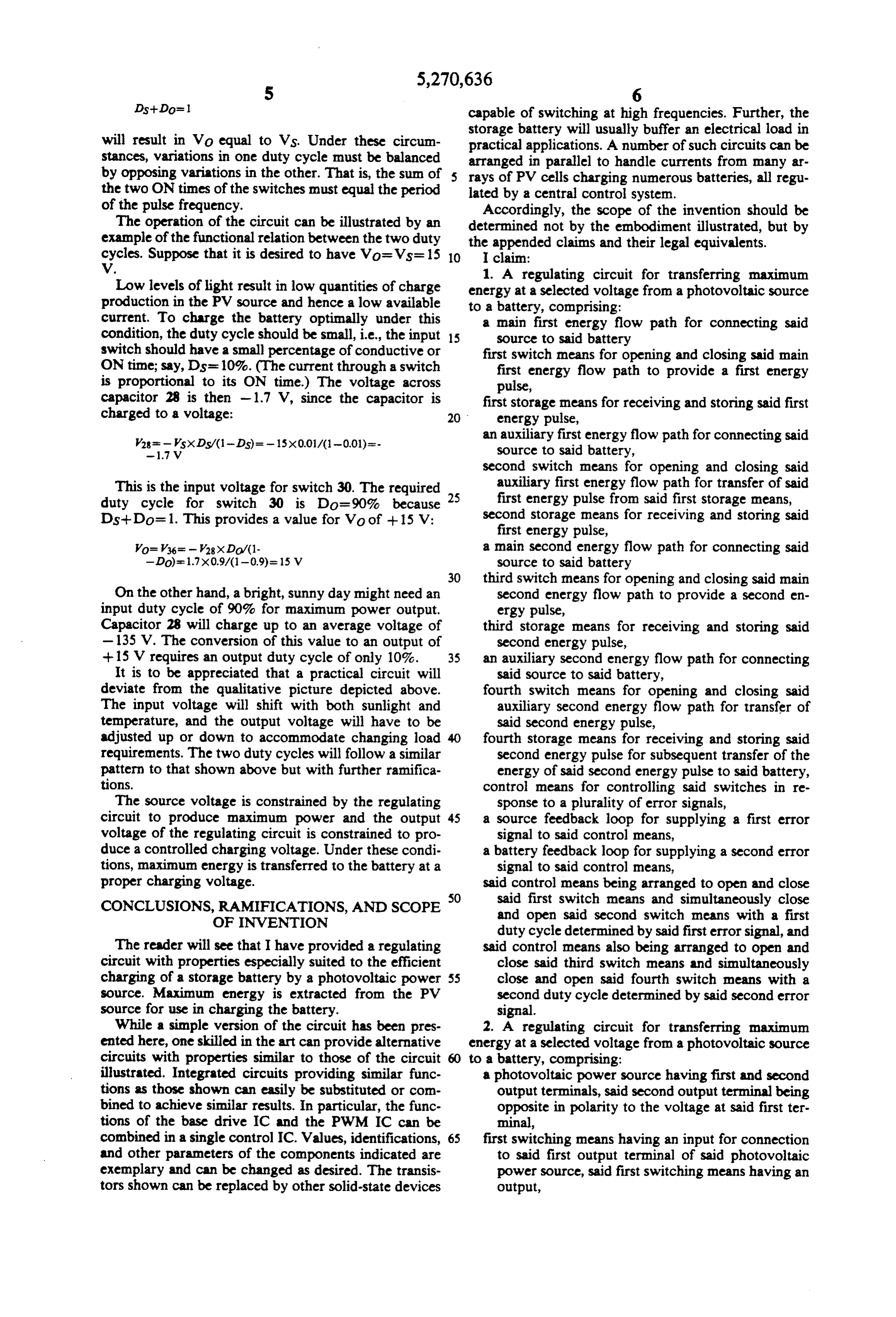
It is, therefore, a primary object of the present inven two transistors 22 and 30 operating as synchronized tion to provide an improved photovoltaic charge-con switches, two inductors 24 and 32, two diodes 26 and trol system, specifically one which increases the effi 34, and two capacitors 28 and 36.
ciency of energy transfer from a PV source to a battery. The emitter of transistor 22 is connected to the top or Other objects are to provide such a system with an positive (--) output terminal of module 20; the other improved coupling network connecting the PV source 65 (botton) terminal of module 20 is grounded. The collec to the battery, and to provide such a network where the tor of transistor 22 is connected to the cathode of diode conversion efficiency is improved by using a regulator 26, and to one side of inductor 24. The bases of transis whose output voltage matches the charging require tors 22 and 30 are connected to output lines D1 and D2
Page 4
of a base drive amplifier circuit 40, described infra. The tion to be made in Vs. The average current through other terminal of inductor 24 is grounded. The anode of transistor 22 is varied by changing its conduction time diode 26 is connected to the emitter of transistor 30 and to increase or decrease the flow as needed to give the to one side of capacitor 28, the other side of which is required Vs. Transistor 22 is pulsed on and off at a high grounded. The collector of transistor 30 is connected to frequency (e.g., 25 kHz) by PWM 42. Thus, Vs tracks the anode of diode 34 and to one side of inductor 32. the value of source voltage required for maximum The other side of inductor 32 is grounded. The cathode power output. The source is thereby regulated for opti of diode 34.joins one side of capacitor 36 to load 38. The mal performance with changing insolation and tempera other side of capacitor 36 is grounded, as is the second tle.
side of the load. The positive terminal of reference cell 10 Independent control of the voltage supplied to the 20A is connected to PWM 42 and the negative side of battery is needed for effective energy storage. Charge 20A is grounded. should be delivered to the battery at a voltage exceed PWM 42 is an integrated circuit (IC) which regulates ing the battery voltage by a volt or two, depending on the flow of charge from source to load by controlling the state of charge of the battery. This constraint estab the conduction times of transistors 22 and 30. To do so, 15 lishes a window or range for the charging voltage. PWM 42 must monitor the input and output voltages as Controlling the conduction time of transistor 30 will well as the voltage of the reference cell. The voltage ensure that the charging voltage lies within this range. across source 20, V is sampled by a connection from Here, output voltage Vo is compared to an internal the positive terminal of PV source 20 to one of the voltage reference provided by PWM 42. PWM 42 gen lefthand inputs of PWM 42. The output voltage of the erates a resulting error signal which controls the con coupling circuit, Vo, is a feedback voltage which is duction time of transistor 30 in a manner similar to that sensed through a connection from the positive terminal used for transistor 22. Thus, the circuit regulates the of the load to the righthand input terminal of PWM 42. average current through transistor 30 to control the The reference voltage, VR, is obtained through a con battery charging voltage.
nection from the positive terminal of reference cell 20A 25 The switching network depicted in the drawing fig to the other lefthand input terminal of PWM 42. ure is composed of two similar sections. The input sec PWM 42 is a dual pulse-width modulation control tion comprising transistor 22, inductor 24, diode 26, and circuit, type TL1451ACN, manufactured by Texas In capacitor 28 is one part and the output section compris struments. It contains all the functions necessary to ing transistor 30, inductor 32, diode 34, and capacitor 36 control two independent switches. PWM 42 compares 30
Vs and VR to generate a train of output pulses on line is aThe second part.
operation of the input section is briefly summa
CH1 which controls the percentage of ON time of tran rized. While switch 22 is conductive, energy is deliv sistor 22. This circuit is a source feedback loop. At the ered from source 20 and stored in inductor 24. When same time, it compares Vo with a fixed internal refer switch 22 opens, inductor 24 tries to sustain the decay ence voltage to generate a second train of output pulses ing magnetic field by generating a back emf. Diode 26
on line CH2 which controls the percentage of ON time becomes forward biased and switches into conduction. of transistor 30. The latter circuit is a battery feedback The resultant pulse of current transfers the energy loop. The pulse repetition rate in each case is a fixed stored in inductor 24 to capacitor 28. The switching frequency of 25 kHz.
Two signals of the proper widths are supplied to a 40 asequence continues as capacitor voltage V2s builds up to steady-state value in which the input current equals base drive circuit IC 40 for transmission as high-current the output current.
pulses to the bases of transistor switches 22 and 30. IC 40 contains four power MOSFET switches controlled DsThe of capacitor voltage is a function of the duty cycle switch 22 and input voltage Vs:
by input storage latches. It translates control logic sig nals (a few mA) from IC 42 of the higher current (sev 45 28= - VSX DS/(1 - DS) eral hundred mA) requirements of switches 22 and 30.
The signal input lines to power IC 40 are labeled chan Note that the capacitor voltage is always negative, since nel 1 (CH1) and channel 2 (CH2), and the output base the duty cycle drive lines, D1 and D2. The outputs onlines D1 and D2 are sufficient to drive transistors 22 and 30. 50 Ds=TON/(Ton--TorF)
OPERATION OF REGULATING CIRCUIT
has only positive values.
The regulating circuit is a further development, im Also of consequence is that the capacitor voltage is provement, and enhancement of the circuits in my pre zero for a duty cycle of zero, is infinitely large for a vious patents supra; it permits a more refined control of 55 duty cycle of unity, and is equal in magnitude to the the charging voltage applied to the battery. Specifi input voltage for a duty cycle of . cally, it allows the PV source to supply current at any The output section behaves the same way as the input voltage within the required charging range. Its opera section, with the exception that the input is the negative tion will now be reviewed briefly from this perspective. voltage V2s across capacitor 28 which is converted to a The output voltage and current of PV module 20 positive output voltage across capacitor 36. The output changes continually with insolation (the amount of solar voltage Vois given by radiation) and temperature. Maximum power transfer to the battery can be maintained by adjusting the current Vo= VSDSDov(1-DS)(1-DO) from the source to the battery. The proper value of current is specified by the open-circuit voltage of refer 65 Where Do is the duty cycle of switch 30 in the output ence cell 20A embedded in PV module 20, Source volt section.
age Vs and reference voltage VR are compared continu The condition, ally to produce a difference signal indicating the correc
Page 5
DS.--Do= 1 capable of switching at high frequencies. Further, the storage battery will usually buffer an electrical load in will result in Vo equal to Vs. Under these circum practical applications. A number of such circuits can be stances, variations in one duty cycle must be balanced arranged in parallel to handle currents from many ar by opposing variations in the other. That is, the sum of 5 rays of PV cells charging numerous batteries, all regu the two ON times of the switches must equal the period lated by a central control system.
of the pulse frequency. Accordingly, the scope of the invention should be The operation of the circuit can be illustrated by an determined not by the embodiment illustrated, but by example of the functional relation between the two duty the appended claims and their legal equivalents. cycles. Suppose that it is desired to have Vo=Vs=15 10 I claim:
V. 1. A regulating circuit for transferring maximum Low levels of light result in low quantities of charge energy at a selected voltage from a photovoltaic source production in the PV source and hence a low available to a battery, comprising:
current. To charge the battery optimally under this a main first energy flow path for connecting said condition, the duty cycle should be small, i.e., the input 15 source to said battery switch should have a small percentage of conductive or first switch means for opening and closing said main ON time; say, Ds=10%. (The current through a switch first energy flow path to provide a first energy is proportional to its ON time.) The voltage across pulse, capacitor 28 is then -1.7 V, since the capacitor is first storage means for receiving and storing said first charged to a voltage: 20 energy pulse, an auxiliary first energy flow path for connecting said source to said battery, second switch means for opening and closing said
This is the input voltage for switch 30. The required auxiliary first energy flow path for transfer of said duty cycle for switch 30 is Do=90% because 25 first energy pulse from said first storage means, Ds--Do= 1. This provides a value for Vo of +15 V: second storage means for receiving and storing said first energy pulse, a main second energy flow path for connecting said source to said battery 30 third switch means for opening and closing said main
On the other hand, a bright, sunny day might need an second energy flow path to provide a second en input duty cycle of 90% for maximum power output. ergy pulse,
Capacitor 28 will charge up to an average voltage of third storage means for receiving and storing said - 135 V. The conversion of this value to an output of second energy pulse, --15 V requires an output duty cycle of only 10%. 35 an auxiliary second energy flow path for connecting It is to be appreciated that a practical circuit will said source to said battery, deviate from the qualitative picture depicted above. fourth switch means for opening and closing said The input voltage will shift with both sunlight and auxiliary second energy flow path for transfer of temperature, and the output voltage will have to be said second energy pulse, adjusted up or down to accommodate changing load fourth storage means for receiving and storing said requirements. The two duty cycles will follow a similar second energy pulse for subsequent transfer of the pattern to that shown above but with further ramifica energy of said second energy pulse to said battery, tions. control means for controlling said switches in re The source voltage is constrained by the regulating sponse to a plurality of error signals, circuit to produce maximum power and the output 45 a source feedback loop for supplying a first error voltage of the regulating circuit is constrained to pro signal to said control means, duce a controlled charging voltage. Under these condi a battery feedback loop for supplying a second error tions, maximum energy is transferred to the battery at a signal to said control means, proper charging voltage. said control means being arranged to open and close
CONCLUSIONS, RAMIFICATIONS, AND SCOPE
50 said first switch means and simultaneously close
OF INVENTION and open said second switch means with a first duty cycle determined by said first error signal, and
The reader will see that I have provided a regulating said control means also being arranged to open and circuit with properties especially suited to the efficient close said third switch means and simultaneously charging of a storage battery by a photovoltaic power 55 close and open said fourth switch means with a source. Maximum energy is extracted from the PV second duty cycle determined by said second error source for use in charging the battery. signal.
While a simple version of the circuit has been pres 2. A regulating circuit for transferring maximum ented here, one skilled in the art can provide alternative energy at a selected voltage from a photovoltaic source circuits with properties similar to those of the circuit 60 to a battery, comprising:
illustrated. Integrated circuits providing similar func a photovoltaic power source having first and second tions as those shown can easily be substituted or con output terminals, said second output terminal being bined to achieve similar results. In particular, the func opposite in polarity to the voltage at said first ter tions of the base drive IC and the PWM IC can be minal, combined in a single control IC. Values, identifications, first switching means having an input for connection and other parameters of the components indicated are to said first output terminal of said photovoltaic exemplary and can be changed as desired. The transis power source, said first switching means having an tors shown can be replaced by other solid-state devices output,
Page 6
first magnetic energy storage means having an input 8. The switching circuit of claim 2 wherein said sec connected to said output of said first switching ond magnetic energy storage means is a second induc means and an output for connection to said second to.
output terminal of said photovoltaic power source, 9. The switching circuit of claim 2 wherein said second switching means having an output also con fourth switching means is a second diode. nected to said output of said first switching means 10. The switching circuit of claim 2 wherein said second electric energy storage means is a second capac and to said input of said first magnetic energy stor itor.
age means, said second switching means having an 11. The switching circuit of claim 2 wherein said input, first electric energy storage means having an output O control
means is a pulse-width modulator.
switching circuit of claim 2 wherein said connected to said input of said second switching second switching means is a third transistor. means and an input connected to said second termi 13. The switching circuit of claim 2 wherein said nal of said photovoltaic source, third switching means having an output connected to fourth switching means is a fourth transistor. 14. A circuit for transferring maximum available en said output of said first electric energy storage 15 ergy at selected voltage from a photovoltaic source to a means, said third switching means having an input, battery to be charged, comprising:
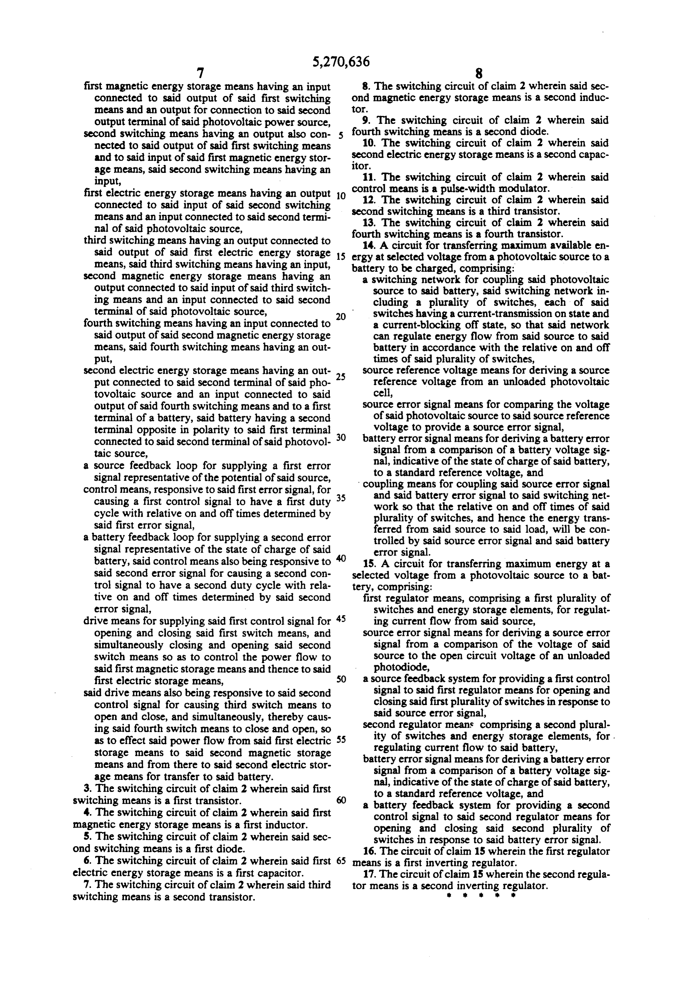
second magnetic energy storage means having an a switching network for coupling said photovoltaic output connected to said input of said third switch source to said battery, said switching network in ing means and an input connected to said second cluding a plurality of switches, each of said terminal of said photovoltaic source, switches having a current-transmission on state and fourth switching means having an input connected to 20 a current-blocking off state, so that said network said output of said second magnetic energy storage can regulate energy flow from said source to said means, said fourth switching means having an out battery in accordance with the relative on and off put, times of said plurality of switches, second electric energy storage means having an out 25 source reference voltage means for deriving a source put connected to said second terminal of said pho reference voltage from an unloaded photovoltaic tovoltaic source and an input connected to said cell, output of said fourth switching means and to a first source error signal means for comparing the voltage terminal of a battery, said battery having a second of said photovoltaic source to said source reference terminal opposite in polarity to said first terminal voltage to provide a source error signal, connected to said second terminal of said photovol 30 battery error signal means for deriving a battery error taic source, signal from a comparison of a battery voltage sig a source feedback loop for supplying a first error nal, indicative of the state of charge of said battery, signal representative of the potential of said source, to a standard reference voltage, and control means, responsive to said first error signal, for 35 coupling means for coupling said source error signal causing a first control signal to have a first duty and said battery error signal to said switching net work so that the relative on and off times of said cycle with relative on and off times determined by plurality of switches, and hence the energy trans said first error signal, ferred from said source to said load, will be con a battery feedback loop for supplying a second error trolled by said source error signal and said battery signal representative of the state of charge of said error signal.
battery, said control means also being responsive to 15. A circuit for transferring maximum energy at a said second error signal for causing a second con selected voltage from a photovoltaic source to a bat trol signal to have a second duty cycle with rela tery, comprising:
tive on and off times determined by said second first regulator means, comprising a first plurality of error signal, switches and energy storage elements, for regulat drive means for supplying said first control signal for 45 ing current flow from said source, opening and closing said first switch means, and source error signal means for deriving a source error simultaneously closing and opening said second signal from a comparison of the voltage of said switch means so as to control the power flow to source to the open circuit voltage of an unloaded said first magnetic storage means and thence to said photodiode, first electric storage means, 50 a source feedback system for providing a first control said drive means also being responsive to said second signal to said first regulator means for opening and control signal for causing third switch means to closing said first plurality of switches in response to open and close, and simultaneously, thereby caus said source error signal, ing said fourth switch means to close and open, so second regulator means comprising a second plural as to effect said power flow from said first electric 55 ity of switches and energy storage elements, for. storage means to said second magnetic storage regulating current flow to said battery, means and from there to said second electric stor battery error signal means for deriving a battery error age means for transfer to said battery. signal from a comparison of a battery voltage sig 3. The switching circuit of claim 2 wherein said first nal, indicative of the state of charge of said battery, switching means is a first transistor. to a standard reference voltage, and a battery feedback system for providing a second 4. The switching circuit of claim 2 wherein said first control signal to said second regulator means for magnetic energy storage means is a first inductor. opening and closing said second plurality of 5. The switching circuit of claim 2 wherein said sec switches in response to said battery error signal. ond switching means is a first diode. 16. The circuit of claim 15 wherein the first regulator 6. The switching circuit of claim 2 wherein said first 65 means is a first inverting regulator. electric energy storage means is a first capacitor. 17. The circuit of claim 15 wherein the second regula 7. The switching circuit of claim 2 wherein said third tor means is a second inverting regulator. switching means is a second transistor.
Provenance
- Collection
- Cited prior art
- Original PDF
- patentimages.storage.googleapis.com →
- Filed
- 1992-02-18
- Pages
- 6
- Method
- pdftotext (the PDF's own text layer) + pdftoppm 300dpi page scans
- Source
- Google Patents bibliographic record
- Granted
- 1993-12-14
- Inventors
- Donald L. Lafferty
- Transcribed from
- patentimages.storage.googleapis.com →