patent · US5007993
Electrolytic processing apparatus and method with time multiplexed power supply
16 April 1991
Page 1 — bibliographic record
United States Patent (19) (11) Patent Number: 5,007,993 Hu et al. 45) Date of Patent: Apr. 16, 1991 54 ELECTROLYTIC PROCESSINGAPPARATUS FOREIGN PATENT DOCUMENTS
AND METHOD WITH TIME MULTIPLEXED
POWER SUPPLY 0647363 2/1979 U.S.S.R. ....................... ... 204/231 0771198 10/1980 U.S.S.R. ... ... 204/231 (76) Inventors: Harry F. Hull, Rau Sao Benedito, 0775197 10/1980 U.S.S.R. .............................. 204/231 761, 04735 Sao Paulo; Ivan P. Da Primary Examiner-Donald R. Valentine
Silva, R. Dos Mainas, 30, 09790 Sao Attorney, Agent, or Firm-Renner, Otto, Boisselle &
Brazil
(21) Appl. No.: 375,605 Computerized apparatus for electrolytic processing of materials, includes an electrolytic processing bath, plu 22 Filed: Jul. 5, 1989 ral first electrodes, at least one second electrode, and a computerized power supply for supplying time multi plexed power to the electrodes. The power supply may
Related U.S. Application Data include a pulse width modulator or a pulse position (63) Continuation-in-part of Ser. No. 368,666, Jun. 20, 1989. modulator and is operative to control the relative amounts of time that the respective electrodes are ener 51 Int. Cl. ...................... C25D 17/00; C25D 21/12 gized for electroplating, electropolishing, and the like. 52 U.S. C. .................................... 204/228; 204/231; Current control and bath composition control are pro 204/406 vided. Plural baths may be monitored and/or controlled (58) Field of Search ........................ 204/228, 231, 406 by a single computer control. A method for electrolytic processing of materials includes placing plural first elec (56) References Cited trodes in an electrolytic processing bath, placing at least one second electrode in such bath, and using a computer
3,875,030 4/1975 Richards et al. ............... 204/228 X is supplied between at least one of such first electrodes 4,100,036 7/1978 Rode et al. ..................... 204/228 X and such at least one second electrode.
4,749,460 6/1988 Komoto et al. ................ 204/228 X 32 Claims, 7 Drawing Sheets
POWER SUPPLY
Page 2
Drawing sheet — no readable text.
Page 3
Drawing sheet — no readable text.
Page 4
Drawing sheet — no readable text.
Page 5
Drawing sheet — no readable text.
Page 6
Drawing sheet — no readable text.
Page 7
START
ENTER PARAMETERS FROM KEYBOARD 4O2
LOAD
VALUES FROM
DISK ?
CHECK VALUES FOR SLAVE
COMPUTE VALUES FOR SLAVE 4O6
SEND VALUES TO SLAVE 4O7
REPEAT FOR OTHER SLAVE CIRCUITS
NEW
VALUES
RECEIVED PERFORMANCLARY FUNCTIONS
DISPLAY, GENERATE REPORTS,
KBD, ?
Page 8
Drawing sheet — no readable text.
Page 9
the electrolytic plating bath to obtain the desired con
ELECTROLYTIC PROCESSINGAPPARATUS AND stituency or relative concentrations of plating materials METHOD WITH TME MULTIPLEXED POWER on the article intended to be plated. For example, to SUPPLY obtain a plated coating of an alloy of zinc and nickel on a metal article, say of a constituency of 88% zinc 12% 3. REFERENCE TO RELATED APPLICATION nickel, it is necessary that the relative amounts of such The instant application is a continuation-in-part of zinc and nickel ingredients in the electrolytic bath beat co-pending U.S. Pat. application Ser. No. 07/368,666, approximately a 62/38 ratio or some other known ratio filed June 20, 1989. that is altered according to some function, such as a 10 function of the ionic nature of the respective ingredients
TECHNICAL FIELD that is representative of the tendency of such material to The present invention relates generally to electrolytic plate onto the cathode/article, the operative efficiency processing of materials, for example, electroplating and, of the anode(s) and/or cathode, etc., as is known. For more particularly, to alloy plating. example, it is known that one material may plate more
BACKGROUND readily than another due to the fact that there are more free electrons available in one than in the other or there
In the field of electroplating an article intended to be is some difference between the ions as they travel plated is placed in an electrolytic bath. The plating through the electrolytic plating bath from the anode to material, such as gold, zinc, nickel, silver or other mate the cathode.
rial or a combination of materials intended to be plated However, as the concentration of one ingredient onto the article, is dissolved in or is otherwise conveyed relative to the other (others) in the electrolytic plating into an electrolyte which forms the electroplating bath. bath changes, regardless of whether such concentration Often the plating material is derived from one or more change is due to anode dissolving or some other reason, anodes positioned in the bath. The anode is coupled to the ratio of those ingredients in the finished plating a power supply and the article intended to be plated also 25 coating will change, which may cause a variation from is coupled to the power supply and serves as the cath ode in the electrolytic plating system. By applying an specifications for the finished plated article. This, of course, is undesirable.
electrical potential difference/voltage between the To alter the concentration relationship of the electro anode and cathode a current flows therebetween through the electrolyte and the plating material mi 30 lytic plating bath to bring it back to the desired specifi cation, it is necessary to increase the amount of one grates to the article intended to be plated. The amount ingredient relative to the other. Such increase some of plating material actually plated onto the cathode/ar times is brought about by changing, say increasing, the ticle intended to be plated is a function of the applied current/potential difference between the anode that is voltage, current flow through the electrolyte and cur
Supplying such ingredient and the cathode. Such a rent density at the article intended to be plated. When 35 change in current, though may cause a change in cur the current density varies at different parts of a particu rent density lar cathode/article, the degree of plating there also will ment at the cathode if a corresponding adjust tend to vary correspondingly. Also, if current is in the current/potential difference between the switched on and off, laminar plating may occur, which other anode and the cathode is not made, which often is undesirable. Laminar plating is a formation of 40 changes the uniform plating thereat and also can cause layers rather than a homogeneous plating. a difference in the amount of one ingredient that is Current typically is a function of applied voltage and plated onto the cathode/article relative to the amount the impedance, as is well known. The impedance typi of the other ingredient that is plated onto the cath cally is a function of the efficiency of the electrodes ode/article. Such a change in current also causes a themselves (including electrochemical equivalents 45 potential difference between the anode whose voltage thereof), of the impedance characteristics of the plating has been changed by increasing current there and the bath, and of the spacing of the electrodes in the bath. other anode which is supplying the other ingredient to It would be desirable to maintain a controlled and the plating bath, thus possibly causing undesirable plat uniform current density at the cathode/article intended ing of the first ingredient onto the other anode, which in to be plated in order to achieve a desired controlled, 50 turn can cause an undesirable shift in operation, anode uniform plating thereof. efficiency, and/or concentration in the electrolytic plat One type of alloy plating uses the anodes themselves ing bath.
to contribute to the composition of the bath. In such In other types of electroplating ingredients are di case plural plating materials are applied to the article rectly added to the bath to obtain plating material intended to be plated as an alloy or mixture of such 55 therein. The invention is useful in such plating tech plating materials. The problems encountered with non niques.
uniform current density are further complicated by the Another type of electrolytic processing is known as additional factor that the concentration of plating mate electrolytic polishing or simply electropolishing. In rial ingredients may vary with time, voltage, plating electropolishing high points or roughness causing flaws that forms on a particular anode or cathode, polariza in the surface of a material intended to be polished are tion of an anode, efficiency of the anode and/or cath removed to improve smoothness of the surface. In elec ode, current density, etc. For example, in one alloy tropolishing the part intended to be polished is placed in plating system with respect to which the invention will an electrolytic bath and serves as one electrode of the be described in detail below, there may be multiple electropolishing system. A second electrode also is anodes, each of which contributes a separate ingredient 65 placed in the bath. A potential difference of prescribed into the electrolytic plating bath to form the plating polarity is applied between such electrodes so that cur material alloy. The concentration of one plating mate rent flows from the part toward the other electrode. rial relative to the other or others must be maintained in Due to the direction of current flow, the part is referred
Page 10
to as the anode, and the other electrode is referred to as To the accomplishment of the foregoing and related the cathode. Since the high points on the part tend to ends, the invention, then, comprises the features herein concentrate current or at least tend to experience higher after fully described in the specification and particularly current density than the already smoother surface por pointed out in the claims, the following description and tions, material at the high points tends to be removed the annexed drawings setting forth in detail certain with the current flow, thus effecting polishing. The illustrative embodiments of the invention, these being various problems encountered in electroplating also can indicative, however, of but several of the various ways detrimentally affect electropolishing. in which the principles of the invention may be suitably The present invention helps solve the above problems employed.
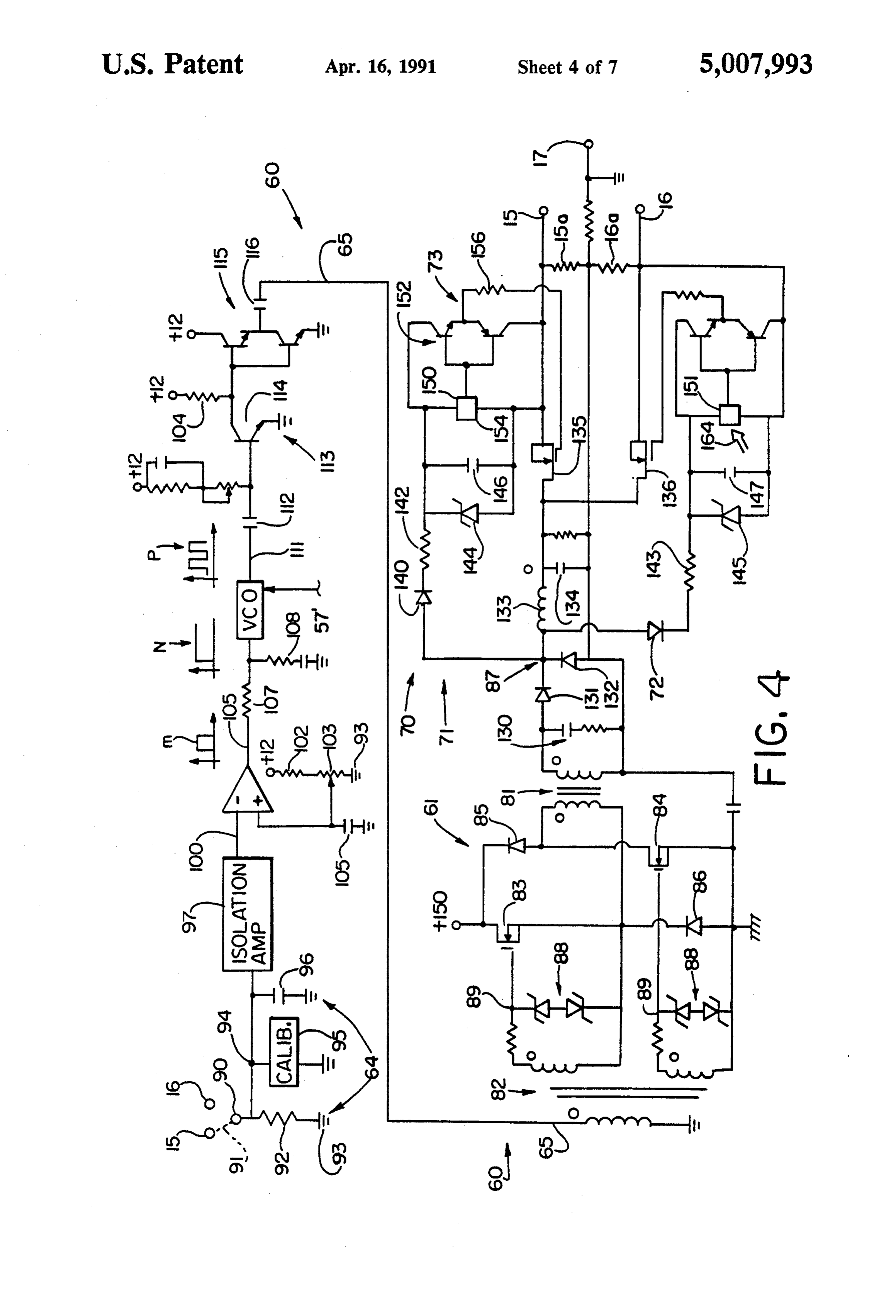
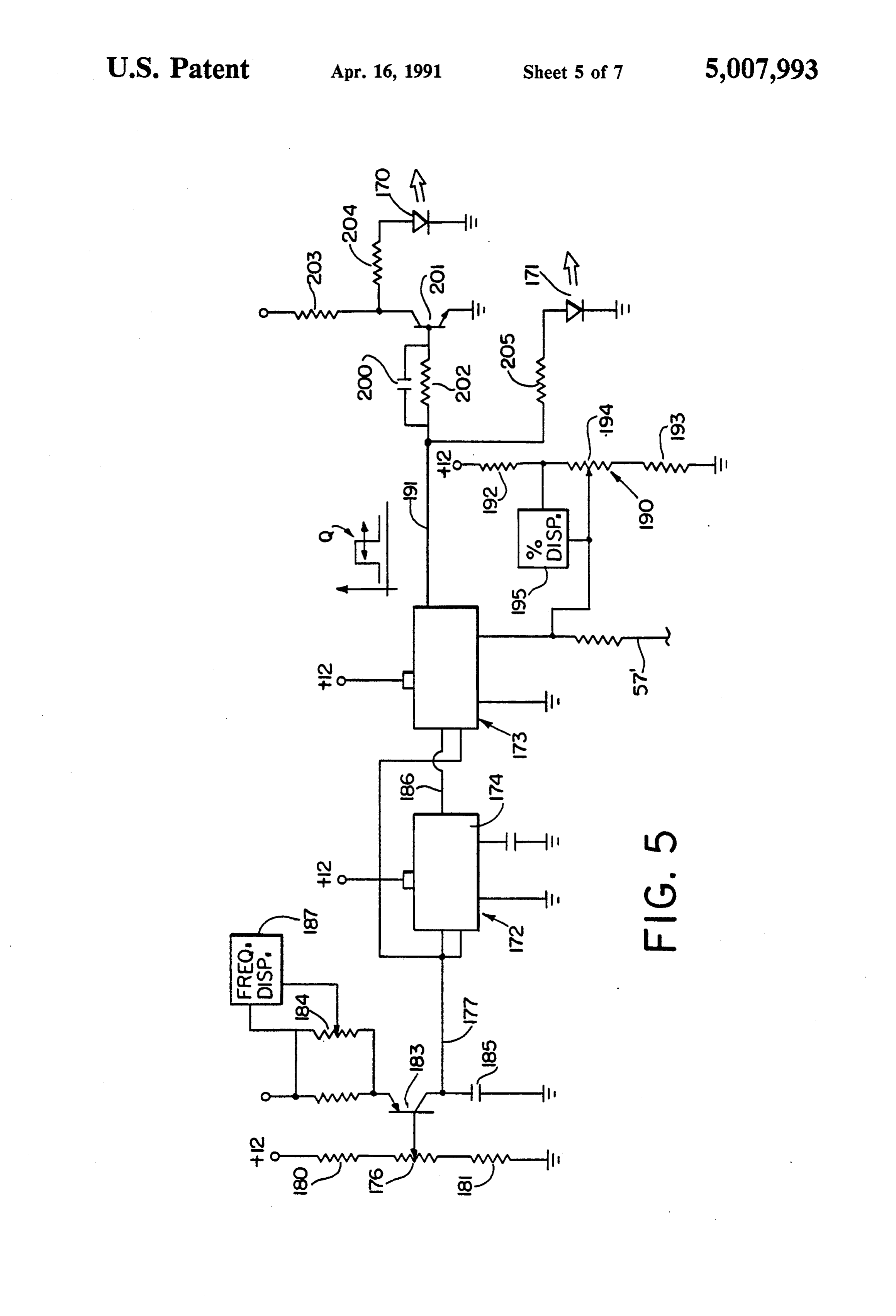
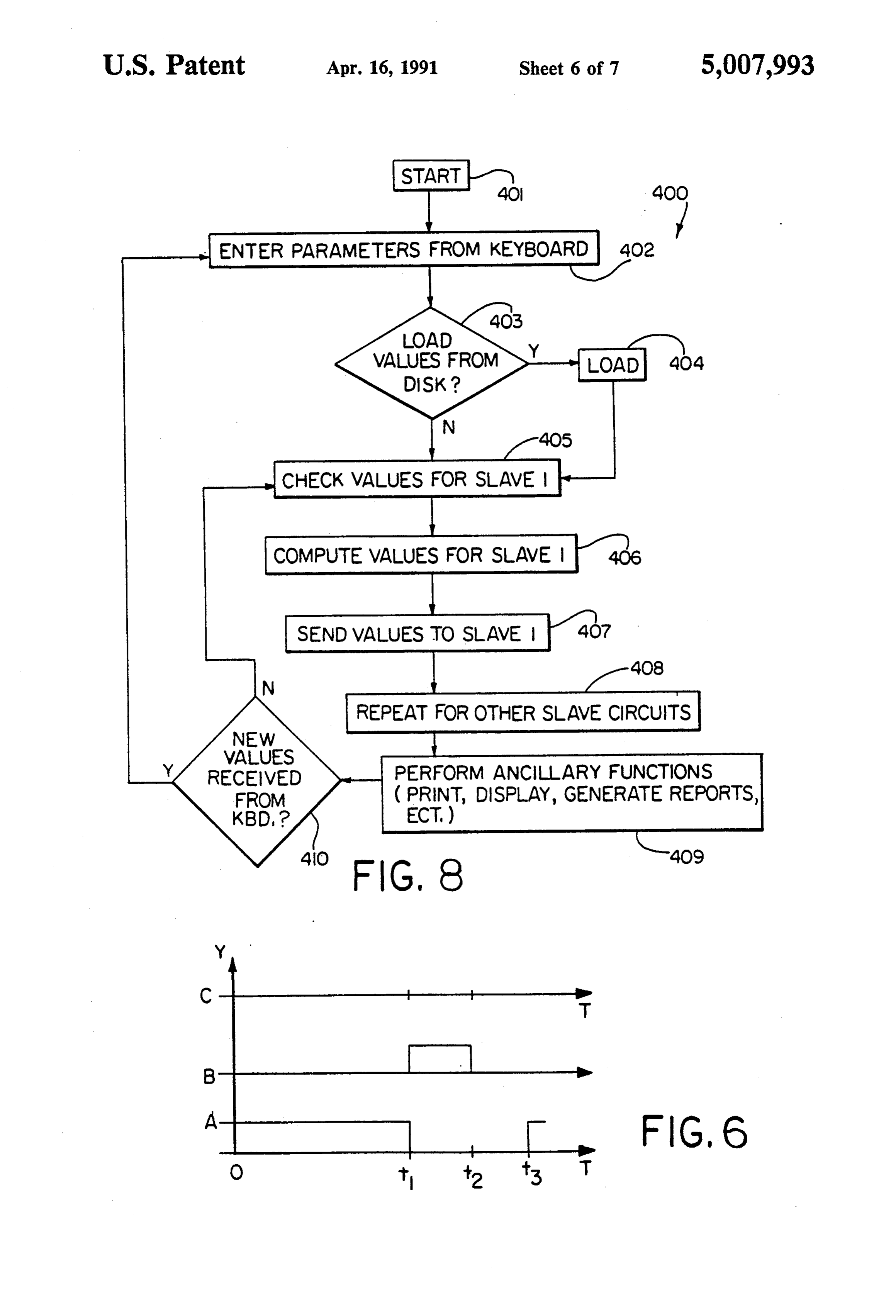
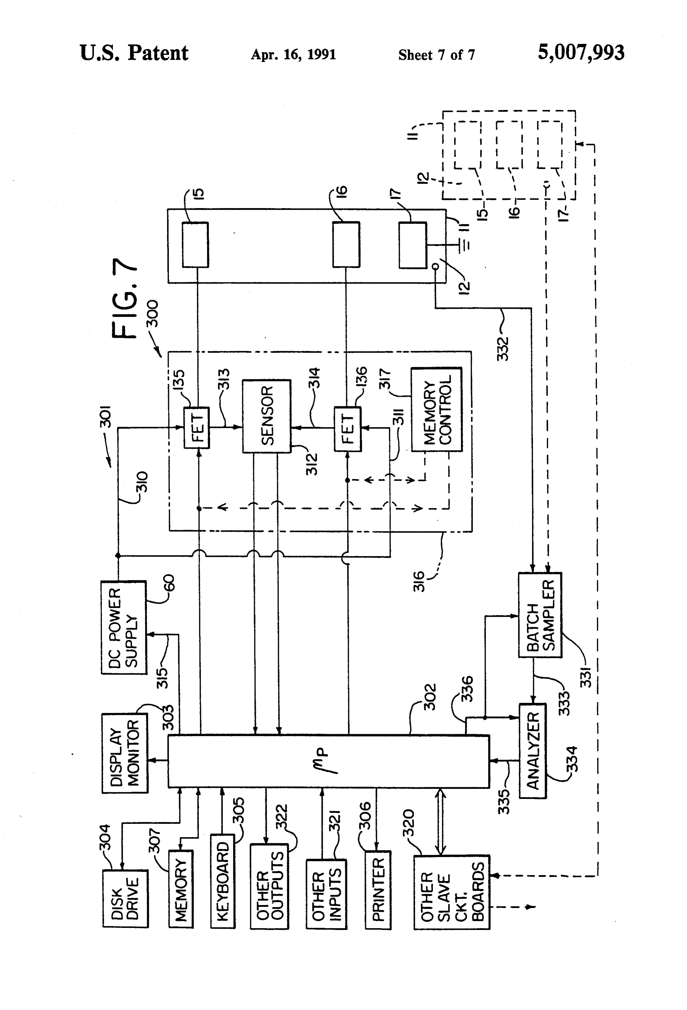
and disadvantages encountered in prior electroprocess O ing systems and methods. BRIEF DESCRIPTION OF THE DRAWINGS Another problem encountered in the past has been In the annexed drawings, the tendency of some electroplating baths to grow or to FIG. 1 is a schematic illustration of an electroplating increase in the amount of a particular ingredient therein apparatus in accordance with the invention; or ratio of that ingredient compared to another. Some 15 FIG. 2 is a schematic electric circuit block diagram of times additives have been added to the bath to control a power supply in accordance with the invention; such growth, and sometimes inert (non-dissolving) elec FIG.3 is a schematic electric circuit block diagram of trodes (anodes) have been used to control such growth. another power supply useful in accordance with the The present invention described below may be used to invention;
control power to such control electrodes, i.e., the inert 20 electrodes, therefore controlling the composition of the of FIGS.
the 4 and 5 are schematic electric circuit diagrams power supply of FIG. 3;
bath.
Further, in the past electrodes formed of an alloy forms used in accordancewaveform diagram showing three wave material have been used to provide the desired concen energization of respective with the invention to provide anodes while providing con tration of alloy ingredients to an electroplating bath. 25 trol of average current;
One example is an alloy of tin and lead. Using the pres FIG. 7 is a schematic block circuit diagram of a com ent invention, though, separate electrodes, one of tin puter controlled electroplating system in accordance and the other of lead, can be controlled to provide the with an embodiment of the invention; and desired concentration of ingredients to the plating bath.
As used herein anode, cathode or electrode may refer 30 tiveFIG. 8 is a computer program flow chart representa of the operation of the computer controlled electro to one anode, cathode or electrode or to a group of plating system of FIG. 7.
anodes, group of cathodes or group of electrodes, as will be evident to those having ordinary skill in the art. DESCRIPTION OF THE PREFERRED BRIEF SUMMARY OF THE INVENTION EMBODIMENT
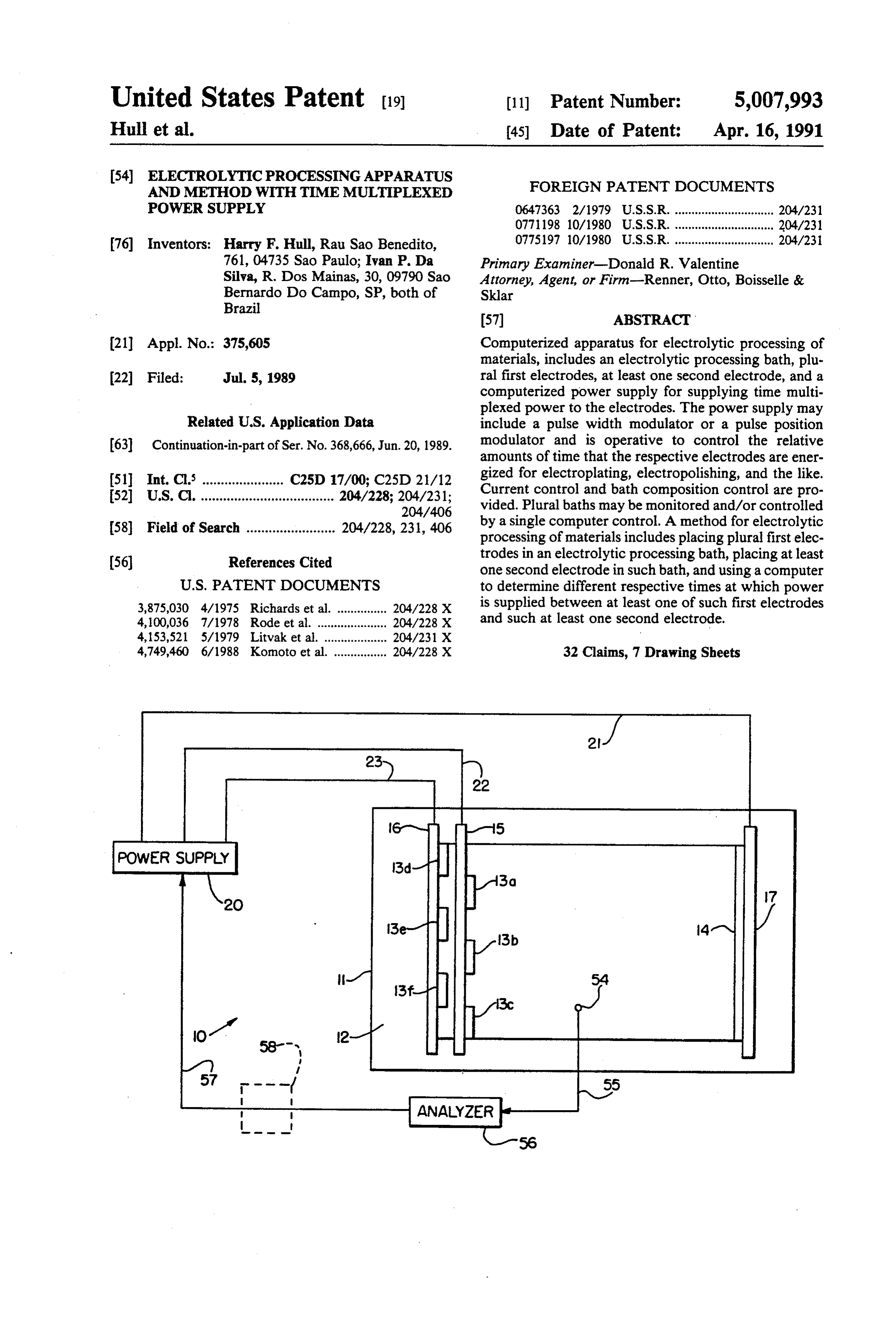
Briefly, according to the present invention an electro Referring, now, in detail to the drawings, wherein lytic processing system and method provide and control like reference numerals designate like parts in the sev power in a time multiplexed fashion. eral figures, and initially to FIG. 1, an electroplating Two examples of time multiplexing according to the apparatus in accordance with the present invention is invention include pulse width modulation of applied 40 generally designated 10. The apparatus 10 includes a signals and frequency modulation (also known as pulse tank 11 containing an electroplating bath 12 in which position modulation) of applied signals. are located plural anodes 13a through 13f. More or According to the invention the time multiplexing fewer anodes may be used. For alloy plating at least two may be used to provide and with providing of current or more of the anodes may be of different materials so control, voltage control, or both. A preferred embodi 45 that such respective anodes deposit such respective ment described in detail below provides current control materials into the electroplating bath 12. The quantity while maintaining substantially constant current density of material (usually metal) deposited by an electrode at the cathode. (typically the anode) in an electroplating bath is a func According to another aspect of the invention the tion of the anode efficiency, the number of coulombs or concentration of ingredients, such as those derived from 50 coulomb-seconds, the bath composition, and/or the electrodes, can be controlled using the time multiplex electro-chemical nature of the material of which the ing control features. electrode is constituted. The material of which such Most desirably, the invention provides a variety of bath is formed may be a conventional electrolyte. The control functions and/or capabilities while maintaining material of which such anodes are formed may be con constant or substantially constant current density at the 55 ventional materials used for electroplating; exemplary cathode to help assure uniformity of plating. materials are zinc and nickel. Other ingredients, addi Various other features of the invention, as are de tives and the like also may be included in the bath as is scribed herein, may be employed in electrolytic pro conventional.
cessing systems and processes, such as in electroplating, Placement of the anodes in the bath 12 may be ac and especially in alloy plating, in electropolishing and in 60 cording to usual convention as a function of deposition other systems. of a plated coating on a cathode 14. The cathode 14 in The foregoing and other objects, features, aspects fact preferably is the article intended to be coated. The and advantages of the present invention will become cathode 14 may be a single cathode or may represent more apparent as the following description proceeds. It several cathodes.
will be appreciated that while a preferred embodiment 65 If the apparatus 10 were used for electropolishing, for of the invention is described herein, the scope of the example, then the part to be polished would be the invention is to be determined by the claims and equiva anode and the other electrode(s) would be the cath lents thereof. ode(s), as is well known.
Page 11
In the preferred embodiment several of the anodes ing voltage between the cathode 14 and the first group 13a-13a are supported from a common electrically con of anodes 13a-13a and causing current flow therebe ductive support anodes 13d-13fare supported from a tween; and for the same or a different length of time, but second common electrically conductive support bar 16. in any event at a different moment in time, a voltage is The support bars 15, 16 may be of copper or other 5 applied between the conductors 21 and 23 thereby pro conventional material. The anodes 13a-13a may be of viding a voltage between the cathode 14 and the second nickel and the anodes 13d-12fmay be of zinc More or group of anodes 13d-13f and causing current flow fewer anodes may be used and they may be of more therebetween. Also, according to the preferred embodi than two materials when alloy plating, depending on ment of the invention, current control is provided so the nature of the plating material. Also, if desired, the 10 that the current flow preferably remains constant, re anodes may be of the same material when the plating is gardless of whether it is flowing between the cathode to be of only one material, i.e. an embodiment of the and the first group of anodes or between the cathode invention in which the plating may not necessarily be and the second group of anodes. Therefore, the current alloy plating. Further, one or more of the electrodes density at the cathode remains constant when current is may be inert or non-dissolving, especially when used to 15 applied.
control growth of an ingredient in a bath and/or to Since the current density at the cathode remains sub effect plating when the plating material is added to the stantially constant, uniform plating in a controlled fash bath from a source other than an anode. ion can be achieved. Indeed, depending on the set up, The cathode 14 may be a single article or several e.g., the positional arrangement, efficiency and size of articles intended to be plated. Such cathode 14 may be the respective anode(s) relative to the cathode(s), differ supported from a single electrically conductive support ent current densities and, thus, plating characteristics, bar 17, for example of copper or other material, or from can be obtained in substantially repeatable fashion. several such bars. As is well known, the anodes and The actual process or electrochemical mechanism of cathode preferably are strategically located in the plat electrolytic plating at the cathode occurs as it does in ing bath 12 relative to each other in order to obtain a 25 conventional electroplating processes. Plating material particular current density at various portions of the in the bath plates on the cathode 14 when current flows cathode and, thus, particular plating characteristics at between anode(s) and the cathode. The actual current those portions. The support bars 15, 16, 17 may be sus and voltage, as well as current density, employed dur pended from rails 18 or by come other conventional ing electroplating using the invention may be selected mechanism used in an electroplating system to position 30 according to conventional electroplating processes. For the electrodes 13, 14 in the plating bath 12. example, the actual current may be from less than one It will be appreciated that although the invention is amp to thousands of amps or even in the million-amp described and illustrated in detail for electroplating an range. The voltages would, of course, be a function of article 14 that remains placed in a single location in the current and impedance between respective electrodes in bath 12, the features of the invention also may be em 35 the plating bath, as is well known. ployed for strip plating. Moreover, by changing the length of time that each An electrical power supply 20 according to the in anode or group of anodes is energized, i.e. has a voltage vention is coupled to supply electrical power to the applied between such anode(s) and the cathode 14 and is anodes and cathode. More specifically, such power the source of current in the bath 12, the concentration supply is coupled by a conductor 21 to the cathode 14 of the ingredient supplied to the plating bath 12 by such and by respective conductors 22, 23 to the respective anode(s) relative to the ingredient supplied by the other groups of anodes that are respectively supported from anode(s) of a different material can be controlled. Espe the electrically conductive support bars 15, 16, as is cially, the ratio of such ingredients in the bath can be illustrated in FIG. 1. The power supply provides a maintained substantially constant. Also, as the effi potential difference or voltage between the cathode 14 45 ciency of one electrode changes, e.g., due to some plat and one group of anodes 13a-13a at one period of time ing material or the like depositing thereon, corrections and between the cathode 14 and the other group of can be made by the power supply 20 altering such re anodes 13d-13fat a different period of time. Preferably spective lengths of time to continue maintaining unifor the power supply 20 supplies current to flow between mity of the plating bath composition. Therefore, the the cathode and the respective anodes to cause plating 50 nature of the alloy plated coating on the cathode can be on the cathode. Since the power supply preferably is closely controlled.
directly coupled to supply power to the electrically As a corollary, if desired, over a period of time, the conductive support bars 15, 16, 17, such support bars concentration of one ingredient in the bath 12 can be also will be referred to below for convenience as the changed relative to the other or other ingredients, power outputs or power output terminals of the power 55 thereby to provide an alloy plated coating on the cath supply. ode that varies in a specified manner through the thick According to the invention, the power supply 20 ness of the coating, for example.
provides electrical power in a time multiplexing type of According to the preferred embodiment, the actual procedure. Such time multiplexing is carried out using length of time that each anode or group of anodes is on, pulse width modulation techniques according to one 60 i.e., energized or receiving power, may be set by the embodiment. Such time multiplexing can be carried out user in order to obtain the desired plating operation using frequency modulation (and/or pulse position and/or plating characteristics on the article being modulation) techniques according to another embodi plated. However, the relative amount of time that each ment. Other time multiplexing techniques that provide anode or group of anodes is on relative to the other(s) functions similar to those disclosed also may be used. 65 can be set or controlled manually or automatically to What preferably is meant by time multiplexing is that maintain a desired composition of the plating bath pref for a particular time period a voltage is applied between erably while maintaining constant current density dur the conductors 21 and 22, for example, thereby provid ing plating, i.e., when power is on.
Page 12
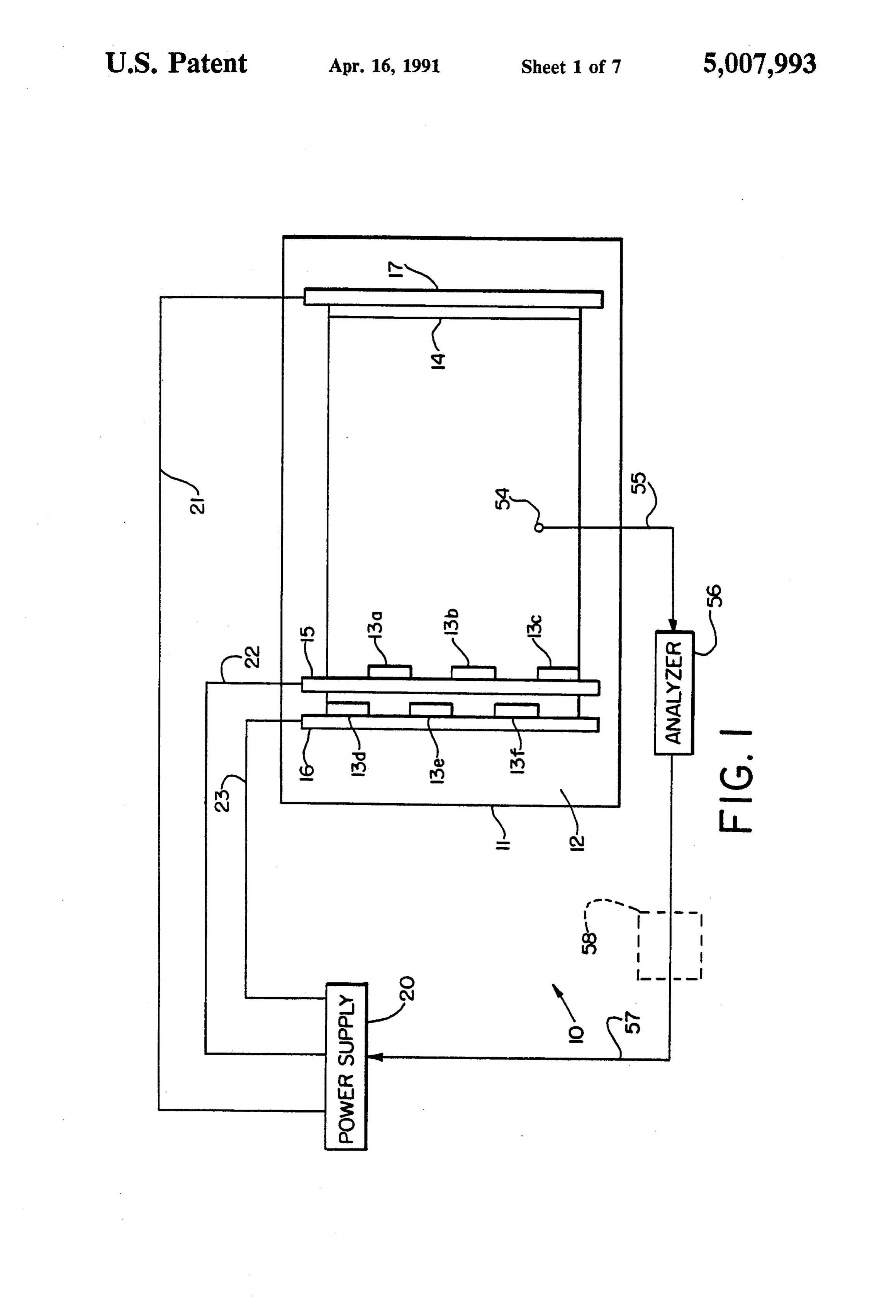
It will be appreciated that although the invention is Each switching circuit 33, 34 preferably is the same. described in detail with respect to alloy plating, features Therefore, only the circuit 33 will be described in detail. of the invention may be employed in other electroplat The circuit 33 includes a switching element 40 that is ing systems, electropolishing systems and other electro able to switch power on and off as it is received from lytic processing systems. the node 32. Such switching element 40 may be for Turning to FIG. 2, a block diagram of a power sup example a conventional power field effect transistor, ply circuit 20 useful in the invention is illustrated. The one type of which is sold under the trademark HEX circuit 20 includes an input rectifier 30 which receives FET or a bridge of FET's coupled to energize the input AC electrical power A. The various exemplary power transformer in conventional manner. Whether signals occurring in the circuit 20 are designated by O the switching element 40 is passing electrical power to alphabet letters. Such signals are illustrated as examples, conductor 41 or not is determined by a conventional but other shapes of signals and other signals also may be pulse width modulator control circuit (PWM) 42 when employed. Also, the signal wave shapes are provided PWM 42 is selectively and sequentially enabled by the only to facilitate the explanation of the circuit, and 15 general control 35. The output signal produced by the values are not indicated. The values would depend on general control 35 is delivered on lines 36, 37 to the the particular apparatus 10 and the power required to PWM circuits 42 in the respective switching circuits 33, accomplish the desired plating function. 34. Such output signal has frequency and duty cycle Preferably such rectifier 30 is a full wave rectifier characteristics that can be adjusted or controlled auto which rectifies the input AC power A (e.g., from the matically or manually, e.g., to determine and to control the composition of the bath 12. The signals on lines 36, utility company) to provide full wave rectified power 37
B. A filter 31 filters the full wave rectified power to to are preferably complementary so that when one is on enable a respective PWM 42, the other is off, and provide a substantially continuous DC signal Chaving a particular amplitude. The rectifier 30 and filter 31 may vice versa.
The PWM 42 may be an integrated circuit part No.
be eliminated in the event that another source of power, 25 3524. Such part includes an oscillator. Therefore, when such as a DC source, were provided to node 32 or even elsewhere in the power supply circuit 20. Also, al the PWM 42 is enabled by the general control 35, such though the invention is described in detail below rela PWM produces an AC output signal on line 38 (line 39 tive to a circuit that operates on a DC power input in the switching circuit 34). An exemplary frequency supplied to node 32, the features of the invention may be 30 for the such AC output signal on lines 38 and 39 may be on order of about 100 KHz. The duty cycle or pulse employed in a circuit that operates based on AC power width input supplied to node 32 by altering the below de currentoforsuch AC signal can be controlled to control scribed various components and interrelationships respective switchingatcircuit voltage the anode(s) energized by the thereof of the power supply switching circuits 33, 34, as 42 thereof is coupled as is 33, 34 in which the PWM described further below.
will be evident to those having ordinary skill in the art. 35 When the PWM 42 in a particular switching Switching circuits 33, 34 preferably are identical or 33,34 no longer is enabled by the general controlcircuit substantially identical. The purpose of the switching stops providing the indicated AC signal; at that 35, it time circuits 33, 34 is to provide voltage between the cathode preferably the other PWM 42 in the other switching 14 and the respective anodes 13. Accordingly, the
Switching circuit 33 provides voltage on conductor 22 circuit circuits produces its AC signal. The respective PWM 42 drive the respective switching elements 40 in to the power output terminal (support) 15 for energiz the switching circuits 33, 34. ing anodes 13a-13c; and the switching circuit 34 pro The output signal D from the switching element 40 is vides voltage on conductor 23 to the power output approximately a square wave signal of relatively high terminal (support) 16 for energizing anodes 13d-13f. frequency compared to the frequency of the input AC Such voltage or energization is with respect to the cath 45 power A. The pulse width of such square wave signal is ode 14, which is coupled to ground or to some other determined by the PWM 42; the frequency may be source of reference voltage potential at power output controlled by the general control 35. Such relatively terminal (support) 16 (not shown in FIG. 2). high frequency square wave signal can be transformed The switching circuits 33, 34 are operated by a gen by a power transformer 43 to a desired output voltage eral control 35, which determines when and for how 50 signal Eof, for example, twenty-four volts peak to peak. long each switching circuit will be enabled to energize As is well known a high frequency signal usually can be the anodes connected thereto. Preferably the general transformed more efficiently than can be a relatively control 35 assures that only one group of anodes will be lower frequency signal, and this preferably is taken into energized at a particular time. consideration in determining the frequency with which The general control 35 may be, for example, a con 55 the switching element is switched.
ventional free running oscillator that is controllable to An output rectifier 44 is coupled to receive the signal determine when and for how long each switching cir E from the transformer 43. The output rectifier 44 pref. cuit is on. The general control 35 also may be some erably is a full wave rectifier which provides a substan other device. The general control 35 may change the tially constant magnitude full wave rectified output relative lengths of time that the switching circuits 33, 34 voltage F. The rectified voltage F is filtered by an out are enabled in order to maintain a desired bath composi put filter 45 to provide a substantially constant DC tion, while the switching circuits are operative to main voltage on line 22 whenever the full wave rectified tain constant or otherwise controlled current density. voltage F is received. Since the switching element 40, Exemplary period of operation of the general control 35 transformer 43, and output rectifier 44 are operating on may be from as long as 15 seconds to as short as 100 65 AC generally square wave signals, the nature of the microseconds, and the relative duty cycles of energiz voltage at the output of the filter 45 supplied to conduc ing the switching circuits 33, 34 would, of course, be tor 22 will be a substantially constant, i.e. unvarying, DC less than that period. voltage relative to the source of ground reference po
Page 13
tential 46, for example taken back at the input filter 31. Other analyzers may be used, as will be appreciated. (The signal G” is shown at output 16 from switchingo Information concerning bath composition may be cou circuit 34. Signals G and G' are out of phase so when pled electrically by electrical connection 57 to the one is on the other is off, as is seen by indicated times to power supply 20 as is seen in FIG. 1. Such electrical to t1 for signal G and times t1 to t2 for signal G'.) connection 57 may be provided as an input to the gen The output filter 45 is coupled by a current sensor eral control 35 to cause the general control to change or feedback line 50 to the PWM 42; and the line 22 is to maintain the relative amounts of time that the switch coupled by a voltage feedback line 51 to the PWM 42. ing circuits 33, 34 are respectively enabled, thereby to Such feedback signals on lines 50, 51 provide control control bath composition. If desired, conventional inter functions to the PWM 42 to help assure that the voltage O face and/or control circuitry, possibly including a com at line 22 is maintained constant and that the current puter, may be coupled between the analyzer 56 and the flow from the energized anodes remains uniform and power supply 20, as is represented at 58, to decode constant as the respective switching circuits 33, 34 ener output information from the analyzer for control use at gize respective anodes coupled to respective power the power supply.
outputs 15, 16. Current and voltage adjustments 52, 53 15 Although the power supply 20 uses a single input may be set by the user and/or automatically to establish rectifier 30 and filter 31, it will be appreciated that each the desired current, current density and/or voltage that of the switching circuits 33, 34 may be supplied with the PWM 42 attempts to maintain in the bath 12. Provi electrical sion for such current and voltage adjust inputs are in associated power from a separate input rectifier and cluded in the 3524 integrated circuit, as is well known. separate supplies ofother 20 filter or circuitry from a common or power. Also, although separate
For example, to maintain a particular current, the cur power transformers 43 are used rent sensor line 50 provides an input to the PWM 42 cuit 33, 34, the invention may useina each switching cir which in turn adjusts the duty cycle of the AC signal on former 43 shared by both circuits 33, 34,power single
trans example line 38, i.e., the percentage or ratio of on time and off being in the power supply circuit 60 of FIG. 3. There time in each on/off cycle of the switching element 40 as 25 fore, the embodiment of FIG. 2 depicts switching of driven by the PWM 42. Current in the bath will be a power before the power transformer and the embodi function of such percentage or ratio. ment of FIGS. 3 and 4 depict switching of power after The power supply 20 operates, as follows. Input power is supplied to the input rectifier 30. That power the power transformer. The power supply 60 may be is full wave rectified by the filter 31 and is provided at 30 substituted for the power supply 20 in the apparatus 10 node 32 to the switching circuits 33, 34. The general of FIG. 1. It will be appreciated that other types of control 35 determines when and for how long each of circuitry may be employed in accordance with the pres ent invention to accomplish the time multiplexed type the switching circuits 33, 34 will be operative to ener gize the respective anodes coupled to the outputs 15, 16 of operation of the electrodes in an electrolytic materi thereof. Ordinarily, when one switching circuit is ener 35 als processing system.
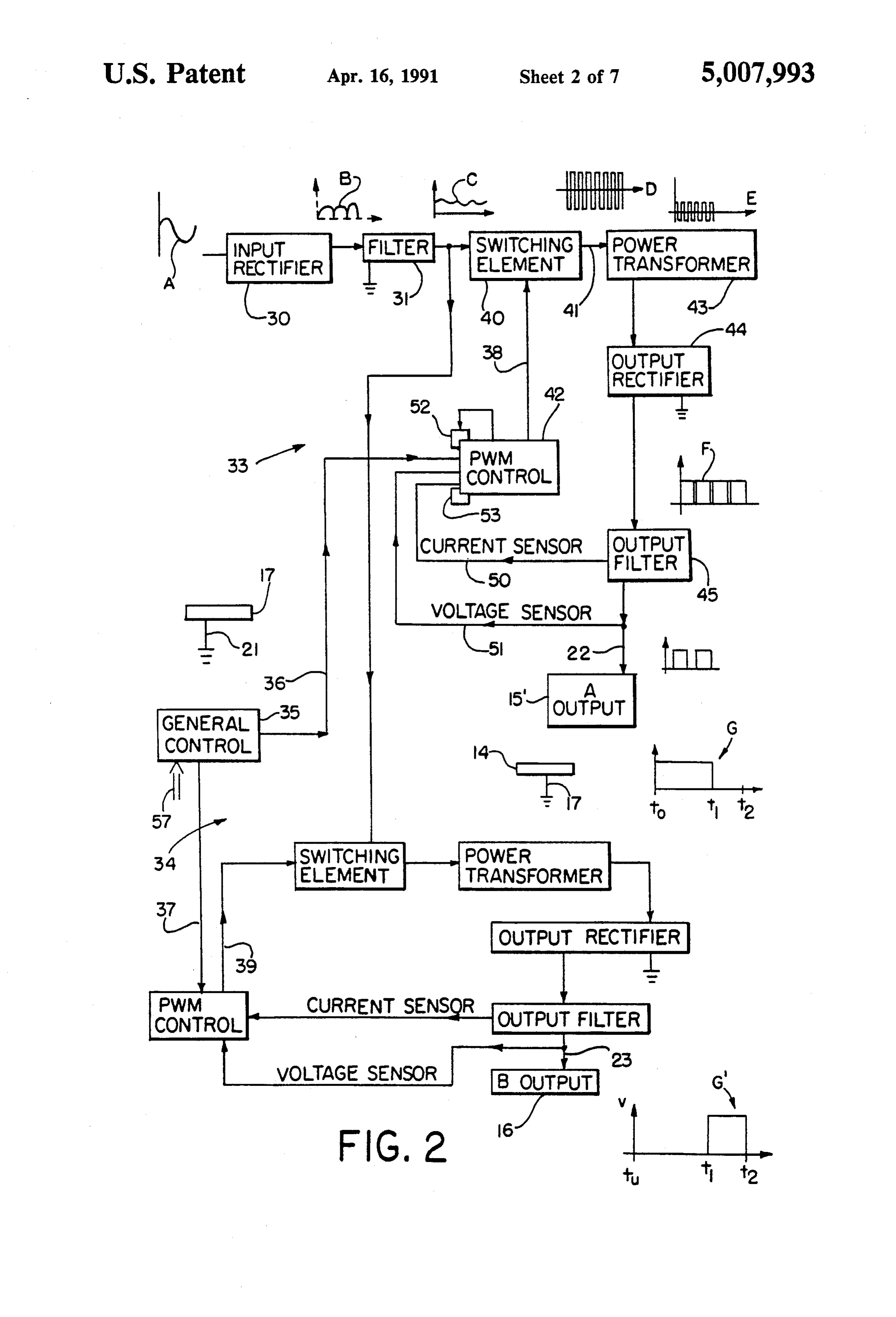
gizing the anodes connected thereto, the other is off, Turning to FIG. 3, another power supply 60, which and vice versa. The pulse width modulator control 42 in may be used in accordance with the present invention, each switching circuit 33, 34 operates the switching to supply power to plural groups of anodes coupled to element 40 thereof when energized to produce the sig power outputs 15, 16, respectively, such as anodes nal D at a pulse width relation determined by the set 13a-c connected to output 15 and anodes 13e-fcoupled tings of the PWM and the current and/or voltage feed to output 16 in FIG. 1. The power supply 60 includes a back on lines 50, 51 and over a period of time deter DC power supply that has both current control and mined by the general control 35. That signal D is trans voltage control capability represented by potentiome formed by the high frequency power transformer 43 ters 62, 63, respectively. A current sensor 64 senses the and is full wave rectified by the output rectifier 44. The 45 current flow at the cathode 14, which is coupled to the full wave rectified signal is delivered via an output filter conductor output 17, and provides an input on line 65 to 45 in each switching circuit to the respective power the DC power supply 61. Such current sensor input output 15 (for switching circuit 33), 16 (for switching may be used by the power supply 60 to maintain con circuit 34). stant current during plating operation. In accordance with the invention the switching cir 50 The power supply 60 includes a dual output circuit cuits 33, 34 are operative so that the current flow from control 70, which is described in greater detail below the respective anodes coupled to the respective outputs with respect to FIGS. 4 and 5. The dual output circuit 15, 16 will be constant and uniform so that the current control 70 is coupled to a pair of output channels 71, 72 density at the cathode remains constant regardless of and determines which is selected at any time to operate the particular output 15 or 16 that is being energized at 55 through respective driver output circuits 73,74 to pro any given time. Further, by altering the amount of time vide power via lines 75, 76 to the respective power that one anode or group of anodes is energized relative outputs 15, 16. Details of the output channels 71, 72 and to the amount of time that another anode or group of of the circuit 60 as a whole are described in detail with anodes is energized, the concentration of ingredients respect to FIGS. 4 and 5. Fundamentally, though, it supplied to the electroplating bath by the respective 60 will be appreciated that the DC power supply 61 pro anodes can be controlled and/or altered. vides a source of DC power to the dual output circuit The present invention is particularly suited to auto control 70. Such circuit control 70 selects which of the mated control, for example, of bath composition. Thus, output channels 71, 72 is to be energized and cooperates a sampling tap 54 may obtain sample material in the bath with the respective driver output circuits 73,74 to sup 12 and deliver such sample continuously or periodically 65 ply power at a desired level to the respective power via a flow line or other means 55 to an analyzer 56. An outputs 15, 16 and, accordingly, to the several anodes, exemplary analyzer may be a conventional X-ray fluo respectively. The power supply 60 may include more rescence analyzer, which detects bath composition. than two output channels.
Page 14
Referring to FIG. 4, a schematic electric circuit dia coupled between the input terminal 90 and the circuit gram of the power supply 60 is illustrated. The power ground 93, and a voltage then is developed on line 94 supply 60 includes a DC power supply portion 61, the representative of the current flowing at the power out dual circuit control 70, driver outputs 73, 74, and a put terminal 15. A conventional display 95 is coupled to current sensor portion 64. Such components cooperate 5 the line 94 to display an indication of the actual current to provide desired power at power outputs 15, 16 cou flow from the selected power output terminal 15 or 16. pled to the respective anodes relative to the power The display 95 preferably includes a calibration circuit output 17 coupled to the cathode. In FIG. 5 is illus to provide full scale calibration. A capacitor 96 con trated a portion of the driver output circuitry, as will be ducts high frequency signals on line 94 to the circuit described further below. 10 ground 93. Moreover, a coupling and isolation amplifier The DC power supply 61 includes a high voltage 97 amplifies the signal on line 94 and provides the same power input 79, for example, of 150 volts or other volt as a voltage on line 100 to a comparator 101, which is age level as may be desired, such as a DC power input formed by an operational amplifier. The voltage on line from a conventional source of DC voltage (not shown), 100 is coupled to the inverting input of the comparator and a chassis ground connection 80. The DC power 15 101. A reference voltage is supplied to the non-invert supply 61 couples power via a transformer 81 to the ing input. The reference voltage is developed across a output channels 71,72. The current sensor circuitry 64 resistor 102 and a potentiometer 103, which are coupled is coupled via a transformer 82 to the DC power supply between the circuit ground and a source of voltage, 61 in order to control the same. The preferred form of such as the Vcc voltage of 12 volts provided form the control is in such a fashion that the current provided at 20 conventional circuit power supply (not shown) coupled the terminals 15, 16 relative to the terminal 17 will re at terminal 104. A capacitor 105 stabilizes the input main substantially constant and uniform regardless of voltage supplied to the non-inverting input of the com which output channel 71, 72 is energized and, accord parator 101. The potentiometer 103 is referred to as the ingly, regardless of whether current is flowing from the current setting potentiometer, for by adjusting that output terminal 15 relative to the cathode terminal 17 or 25 potentiometer, the magnitude of current supplied at the from the output terminal 16 relative to the cathode output terminals 15, 16 can be adjusted (set), as will be terminal 17. evident from the following description. In the DC power supply 61 are included a pair of The output voltage M on line 106 at the output from power field-effect transistors (FET), such as those sold the comparator 101 ordinarily will be a logic 1 or a under the trademark HEXFET, 83, 84 and a pair of 30 logic 0 level, i.e., on or off, depending on whether the diodes 85, 86, which are connected relative to each current at the power output terminal 15, 16, which had other and relative to the two secondaries in the trans been selected by the jumper 91, is greater or is less than former 82 and the primary in the transformer 81 in full the current setting adjustment of the potentiometer 103. wave bridge configuration. The FETs 83, 84 are oper As the current at the selected output terminal 15, for ated such that both are on at the same time or both are 35 example, periodically exceeds or does not exceed that off at the same time. As is evident from the illustration current established in the current setting potentiometer in FIG. 4, by periodically turning the FETs 83, 84 to 103, the signal M will take a characteristic of sometimes conductive or on state, current flows through the pri being on and sometimes being off. The signal M is cou mary of the transformer 81 in one direction, and when pled via a resistor 107 and a resistor-capacitor circuit the FETS 83, 84 are turned off, diodes 85 and 86 demag- 40 108 to the input of a voltage controlled oscillator netize the transformer 81. Depending on the nature of (VCO) 110. The resistor 107 and the RC circuit 108 the signal provided the primary of the transformer 82 cooperate to convert the signal M to a DC voltage level from the current sensor circuitry 64, the magnitude of signal represented at N.
current in the secondary of the transformer 81 is con The voltage controlled oscillator 110 produces an trolled. Therefore, when more or less current is desired 45 AC output signal P on line 111. The frequency of the at one of the power outputs 15, 16, the DC power sup signal P is a function of the magnitude of the voltage of ply 61 increases or decreases the power coupled by the the signal N. Therefore, as the comparator 101 detects transformer 81 which in turn is provided at node 87 for that the current at the selected power output 15, for coupling into the respective output channels 71, 72. The example, is closer to or is further from the desired cur actual signal at node 87 is a pulsating voltage signal. The 50 rent as determined by the setting of the potentiometer frequency of the voltage pulses at node 87 may be 103, the voltage N at the input of the VCO will change changed under control of the feedback current sensor and the frequency of the signal P on line 111 will vary 64 depending on whether more or less current or power correspondingly. Preferably, the voltage controlled is needed at the power output terminals 15, 16. oscillator 110 is a linear voltage controlled oscillator Zener diode circuits 88 may be coupled across the 55 that always provides the signal P such that there is a drain and source electrodes of the FETs 83, 84 for usual 50% duty cycle of the output signal P even though the protective purposes, limiting the voltage drop therebe frequency of the signal P may vary. Therefore, in each tween. Also, resistors 89 may be coupled in circuit with full cycle of positive-going and negative-going portions the secondaries of the transformer 81 and the respective of the signal P, the duration of each positive-going zener diode circuits for conventional protective pur portion will be the same as the duration of each nega pose limiting current in the diodes. tive-going portion for the particular frequency of the To develop the current control signal provided by signal P.
the current sensor circuitry 64 to the DC power supply The signal P is coupled via a capacitor 112 to the 61, an input terminal 90 is coupled to a selected one of input of a transistor circuit 113, which functions in a the power output terminals 15, 16. Either one may be 65 sense as a one-shot multivibrator. The purpose of circuit used or both may be used. For illustrative purposes, a 113 is to prevent saturating the transformer 82. In par jumper 91 is shown connected to the power output ticular, if the frequency of the signal P is large enough, terminal 15. An accurate current sensor resistor 92 is it will operate via the transistor 114 and the pair of
Page 15
amplifying transistors 115 to be coupled through a ca load for the circuit in case the anodes and cathode are pacitor 116 to line 65, thus providing an AC signal to not in the bath when the power supply circuit 60 is on. the primary of transformer 82. The frequency of the The voltage at node 87 is coupled via diodes 140,141, signal on line 65 will be increased or decreased as a resistors 142,143, Zener diodes 144, 145, capacitors 146, function of whether current at the power output 15, for 147 to a photosensitive module 150, 151 of a conven example, requires increasing or decreasing. tional opto-isolator and to a transistor output circuit The multivibrator function of the transistor circuit is 152, 153. Referring to the output channel 71, when a achieved by a bias circuit 120 which includes a resistor light input, which is represented by arrow 154, is sup 121 a capacitor 122, and potentiometer 123. The circuit plied to the photosensor 150, the latter produces a signal 120 and the potentiometer 123 cooperate with the ca 10 on line 155 to provide a signal via the transistor circuit pacitor 112 to assure the length of any pulse delivered 152 and resistor 156 to the line 137 turning on the FET by the transistors 113, 115 to the transformer 82 will be 135. The FET 135 then delivers current to the power short enough that the transformer 82 will not saturate. output terminal 15. Similar operation occurs in the out When the output from the VCO is of high enough put channel 72 when light 164 is provided the photosen frequency, such signal passes through capacitor 112 and 15 sor 151, which then provides a signal on line 165 to directly drives the transistor 114. However, when such cause the transistor circuit 153 to produce a signal via frequency is relatively slow compared to the time con resistor 166 onto the control line 138. The FET 136then stant of the capacitor. 112 and the resistance setting of turns on to provide current to the power output termi potentiometer 123, such capacitor and potentiometer nal 16.
cooperate to limit the pulse width of the signal deliv 20 The optical signals 154, 164 are developed in the dual ered on line 65 to the transformer 82 to one that appears output circuit control 70 portion illustrated in FIG. 5 as having a frequency that is large enough to avoid and, more particularly, in fact are emitted by respective saturation of the transformer. For example, transistor light emitting diodes 170, 171 of respective opto-isola 114 is biased to conduction to hold transistors 115 off. tors that include the respective photosensors 150, 151. When a negative going pulse begins on output 111 from 25 The circuit 70 includes a pair of timing circuits 172,173, VCO 110 (such as the VCO portion of an integrated each of which may include a conventional 555 inte circuit No. 4046), transistor 114 turns off and transistors grated circuit timer 174, 175 connected generally in the 115 turn on sending a signal to transformer 82. If the manner illustrated. The timing circuit 172 determines VCO output on line 111 does not return to a high or the cycle frequency of the dual output circuit control relatively positive level (relative to the mentioned nega 30 70. The timing circuit 173 determines the relative duty tive going pulse), the capacitor 112 charges in time cycle of the two portions of the signal which makes up according to the RC time constant with resistance of an entire cycle; specifically, the timing circuit 173 deter potentiometer 123 to a level that again biases transistor mines what proportion of each complete cycle the light 114 on and transistors 115 off. Such time constant is emitting diode 170 emits light and what proportion of adequately fast to assure that transformer 82 will not 35 the complete cycle the light emitting diode 171 emits Saturate. light.
The pulsating voltage at node 87 is derived from the To establish the cycle frequency, an input circuit 176 output of the secondary of transformer 81, RC filter 130 is coupled via line 177 to an input of the timing circuit and diodes 131, 132. Such pulsations voltage is the 172. The input circuit 176 includes several resistors 180, source of current that will be provided drive outputs 15, 181 and a potentiometer 182, all of which are coupled in 16. Voltage at the node 87 is provided via a conven series between the Vcc power supply 104 and the circuit tional inductor 133 and capacitor 134 LC filter, which ground 93. The wiper arm of the potentiometer 182 is provides a DC voltage level at node 87. Due to the connected to the base of a transistor 183, which in turn operation of the LC filter, the magnitude of the DC is connected in a charging circuit that includes a resistor voltage at the node 87 will be a function of the fre 45 184 and a capacitor 185. Depending on the setting of the quency of the voltage pulses at node 87. The voltage at potentiometer 182 and the values of the resistor 184 and node 87 is supplied to the inputs of a pair of power capacitor 185, such capacitor 185 will charge at a pre FETs 135, 136. The control inputs of the respective scribed rate that will determine the frequency of the FETs are coupled to control lines 137, 138. When a signal produced on the output 186 of the 555 timer 174. signal is on a respective line 137, 138, the respective 50 Current flow through the resistor 184 represents the FET provides to the respective power output terminal frequency of such signal on line 186 and can be moni 15, 16, current flow to energize the respective anodes tored and displayed by a conventional display, such as a coupled to such power output terminals. The driver liquid crystal display, represented at 187. output circuits 73, 74 generate such control signals for The input line 177 and the output line 186 for the 555 delivery on lines 127, 138 to the FETs 135, 136, as now 55 timer 174 are coupled to inputs of the 555 timer 175. will be described. Moreover, a control input circuit 190 is coupled to Since the invention provides for operation of the another input of the 555 timer 175 to determine the circuit 60 in current control mode, whereby the current portion of each full cycle of output signal Q produced output at output terminal 15, for example, is maintained on output line 191 from the 555 timer 175, that is, at a constant due to feedback through the current sensing logic 1 or "on" level and what portion is at a logic 0 or resistor 92 and current sensor circuitry 64, the magni "off' level. The input control circuit includes a series tude of the voltage at node 87 will be a function of the connection of a pair of resistors 192, 193 and a potenti actual load, e.g., the load across the terminals 15 and 17 ometer 194. By adjusting the wiper arm of the potenti (and any additional load, such as that provided by the ometer 194, the percentage or proportion mentioned resistors 15a and 16a). The load across terminals 15, 17 65 can be changed. Since the voltage drop between the is a function of the impedance of the electroplating bath potentiometer wiper arm and one other terminal of such 12 and the spacing of the anodes and cathode. Resistors potentiometer represents such percentage or propor 15a and 16a provide protection by supplying a finite tion, that voltage can be monitored and displayed, for
Page 16
example, in a conventional liquid crystal display, which will increase in the bath relative to another ingredient is represented schematically at 195. supplied by the other less efficient anode. The invention Output line 191 is coupled to a complementary output permits a change in the times that each of the anodes is circuit 200, which decodes the signal Q so as to turn on energized thereby to maintain uniform composition of the light emitting diode 170 to emit light when the the bath.
signal Q exhibits a logic 0 or off state and to turn on the As was mentioned above with respect to the power light emitting diode 171 when the signal Q exhibits a supply 20 in FIGS. 1 and 2, the invention lends itself to logic 1 or on state. The complementary output circuit both automated and manual control. Manual control, 200 includes a transistor 201, which is coupled via an e.g., by setting the current density at potentiometer 103, RC circuit 202 to the line 191, a resistor 203, which is O and relative amounts of energization times for the re coupled to the Vcc voltage source 104, and a resistor spective cathodes or groups of cathods, e.g., by setting 204, which is coupled to the light emitting diode 170. the potentiometer 194, has been described above for the When the signal Q on output line 191 from the 555 timer power supply 60 of FIGS. 3 and 4. Automated control 175 is at logic 0 level, the transistor 201 is not conduct would include the use of a sampling tap 54, analyzer 56 ing; therefore, current can flow from the Vcc source 104 15 and possibly additional interface and/or control cir via resistors 203,204 through light emitting diode 170 to cause the latter to emit light. Since the signal Q is at a cuitry of conventional design 58, that would provide an logic 0 level, the light emitting diode 171 will not emit connectionthewould input to power supply circuit 60. An exemplary be one shown at 57" in FIG. 5 to bias light. However, when the signal Q is at a logic 1 level, the 555 timer 175 causing it to change the relative such signal will bias the transistor 201 to an on or con 20 ducting condition so as to shunt current away from the amounts of of time that the respective electrodes or groups electrodes are energized by power supply 60. An light emitting diode 170, which then will not emit light. other automated control connection may be to the VCO Additionally, when the signal Q is in a logic 1 condition, 110, as is described further below. such signal will operate through resistor 205 to cause Another advantage of the present invention is that light emitting diode 171 to emit light. 25 although the invention is particularly suited for use in
In operation of the power supply 60, the potentiome alloy plating using electrodes of different materials, it is ter 182 (FIG. 5) can be adjusted to determine the fre usefull, too, for plating using electrodes of the same quency that signals are developed in the opto-isolators to drive the respective FETs 135, 136. Adjustment of material and even in circumstances in which the plating the potentiometer 194 (FIG. 5) determines the propor 30 material is furnished the electroplating bath as an addi tion of time that FET 135 is on relative to the time that tive to the bath, i.e., not being directly supplied by a FET 136 is on and, therefore, the proportion that time respective anode. Using the time multiplexing features current is supplied to respective power outputs 15, 16. of the invention, especially also with the constant cur Adjustment of the potentiometer 103 (FIG. 4) deter rent feature, one anode or group of anodes may be mines the magnitude of current actually delivered to the 35 energized for one period of time, and subsequently a power output terminals 15, 16. The current sensor cir different anode or group of anodes may be energized. cuitry 64 and DC power supply 61 cooperate to main During the time that an anode or group of anodes is tain a substantially constant current level, as is set by the deenergized such anode or group may depolarize. The potentiometer 103, at the power output terminals during amount of time that the anodes are deemergized can be plating. 40 determined in the power supply circuit 20 by the gen It will be appreciated from a review of the circuit eral control 35; and the amount of time that the anodes portion 70 of FIG. 4 that the outputs to the opto-isola are deenergized can be determined in the power supply tors are complementary. Therefore, when one light circuit 60 by alteration of the frequency of the VCO output is on, the other is off, and vice versa. An advan 110. Further, if the power supply circuits of the inven tage to the complementary outputs is that the current 45 tion were altered for use to energize respectively and density in the bath may be maintained substantially sequentially three or more anodes or groups of anodes, constant without regard to which anode is being ener then the amount of time that a particular anode or group gized at a particular time. is deenergized can be further increased to facilitate However, it will be appreciated that other means may and/or to enhance depolarization.
be provided for developing the driving signals for the 50 A problem experienced in prior art electroplating FETs 135, 136, either optical or otherwise. Moreover, baths, especially alloy plating baths of the type in which the means for developing the driving signals for the two different types of electrodes are used, has been the FETs 135, 136 may either be coupled in the comple formation of a plated layer on or plating of one anode mentary manner illustrated or may be developed inde relative to another. For example, if both nickel elec pendently. An example of independent developing of 55 trodes and zinc electrodes were used in the bath, and such signals may be achieved by using separate mono both were intended to contribute metal to the bath for stable multivibrators independently controlled by the alloy plating of a cathode, then it has been found that current control circuit 64 and/or by the circuit portion material of one anode sometimes would plate onto the 70, as will be evident to those having ordinary skill in other. Such plating of an anode would change the effi the art. ciency thereof and the general balance of the plating An advantage of the present invention is the ability to system. To accommodate such imbalance, it has been adjust the circuit 60 to compensate for a difference in customary to require that anodes be placed in a plating the efficiency and electrochemical equivalent of the bath and the bath operated for a prescribed period of various electrodes. For example, relative to the cathode time until a balanced condition would exist. A typical one anode may be relatively efficient, say 90 percent 65 procedure to correct such imbalance would be to efficient, and a second anode may less (or more) effi change the voltage applied to one anode relative to the cient, say 80 percent efficient. Over time the ingredient other; but this further exacerbates the imbalance be added to the plating bath by the more efficient anode cause due to a potential difference between such anodes
Page 17
additional plating or a change in plating of one relative for how long a particular anode or group of anodes is to the other or onto the other will occur. energized. Considering a plating system in which only The present invention overcomes the foregoing prob one anode (or group) is used, the duty cycle of applied lem by preferably permitting the deenergized anodes to power can be changed, i.e., to determine for how long float electrically when not energized. Therefore, there in each of a prescribed period the anode is energized. will not be a potential difference or at least will only be Therefore, if such period were selected to be one sec a minimal potential difference between energized and ond and a duty cycle of 0.8 second were selected, then deenergized anodes and/or the impedance in an electri in that period for 0.8 second the anode would be ener cal circuit containing such electrodes will be so rela gized and for 0.2 second the anode would not be ener tively high as to prevent or at least to minimize any 10 gized. During the time that the anode is energized, current flow therebetween and, thus, plating of one preferably current flow is provided to achieve constant relative to the other. current density and plating at the cathode even as the The invention is useful to facilitate depolarization of impedance of the bath, anode efficiency cathode ef. anodes. An anode may form an oxide coating on it. ficiency/conductivity, etc. may change. During the Such coating can reduce the solubility of the anode in 15 time that the anode is deemergized, no plating occurs. the bath, thus reducing anode efficiency. Therefore, the Such control provides control to achieve a particular voltage required to drive that anode to apply the de type of plating, polishing, or other processing, as may sired amount of ingredient to the bath therefrom, in the be desired.
past, has had to be increased. Such oxide coating is due Furthermore, the aforementioned control of duty to a concentration of oxygen at the anode during energi 20 cycle can be used to control average current. This is zation or operation thereof. Using the present invention, true regardless of whether one anode or several anodes one anode or group of anodes may be energized for a are used in the plating system. The amount of plating or particular duration while another anode or group of metal deposited is a function of coulombs. Therefore, if anodes is deemergized. During the period that it/they current is turned off for a duration in a particular period is/are deenergized, the oxygen concentration at such 25 of operation of the plating system, average current and deenergized anode(s) will have time to dissipate in the the amount of coulombs are reduced; and this is accom bath. As a result, the amount of oxide coating that will plished even though when the plating current is on it in accumulate on such anode(s) when subsequently ener fact is supplied at a prescribed constant level. This fea gized will be less than has been experienced in the prior ture further helps to assure accurate control and con electroplating systems. 30 stant characteristics of the plating. Moreover, since the invention can be use both for Extending the features described just above to a mul alloy plating and for single material plating, or for plat tiple anode system and a power supply that uses one ing in which the relative amounts of time that each more output than the number of anodes employed, by electrode or electrode group are energized is the same, varying the amount of time that each of the anodes is a savings in equipment cost can be realized because only 35 energized in a given operational period of the power one power supply may be used to perform both types of supply and the amount of time that the power supply is plating functions. not energizing an anode, the average current also can be Another advantage of the present invention is the controlled while plating by the other anodes is accom ability to prevent so-called creep, growth or increase of plished at constant current. Referring, for example, to a particular ingredient in an electroplating bath. This is 40 FIG. 6, three wave forms A, B, and C are shown occur a particular problem in alkaline zinc plating wherein the ring in a time period T. From time 0 to t1 waveform A anode efficiency can be greater than the cathode effi is on; and a first anode or group of anodes is energized ciency. As is known, inert anodes (also known as non by an output from power supply 60, for example; also, dissolving electrodes) sometimes are placed in an elec waveforms B and C are off and the second and third troplating bath alone or together with anodes that con 45 (the third not being shown in the power supply 60) tribute material to the bath. When the concentration of outputs from the power supply and anodes are not ener an ingredient contributed by the latter anodes or by gized. From time t1 to time t2 waveform B is on and the some other means exceeds a prescribed level or is at respective anode is energized, while the others are de least at a desired level, the inert electrodes are energized energized. Finally, from time t2 to time t3, which ends and the others are deenergized. In this way electroplat 50 the period, none of the waveforms A, B or C is on; and, ing can continue while using up the mentioned ingredi therefore, none of the anodes is energized. Accordingly, ent from the bath after which the ingredient contribut average current is reduced from a circumstance that ing anodes will be energized instead of the inert elec each electrode is energized at some time during the trodes. The present invention is suited for use in such an period such that there would not be any time during environment because the respective power supplies 55 which plating would not be occurring. The actual dura may be switched in time multiplexed fashion to energize tions of the respective waveforms A, B and C can be the ingredient contributing anodes and the inert anodes changed according to the invention thereby to change for respective amounts of time such that the particular average current while still assuring that during plating ingredient that tends to grow in the bath will remain current density is constant.
substantially at a stable concentration in the bath, while The ability to control average current is particularly plating still is carried out at constant current. Moreover, advantageous to maintain a uniform plating from part to the relative amounts of time that such electrodes may be part, especially as the size of the cathode (part) and/or energized can be changed, as was described above, the number of cathodes being plated at one time in a further to change the concentration of the mentioned bath may change.
ingredient in the bath. 65 It is believed that an effective capacitance may occur The present invention provides versatility in control at the interface between an anode and the electrolytic ling the nature of plating onto the cathode. For exam bath in which it is placed. The present invention pro ple, the present invention enables control of when and vides for control of the frequency and pulse width of
Page 18
signals energizing respective anodes. Therefore, the tion of the bath 11 and the system 300, as is conven effect of such capacitance can be controlled, used to tional.
advantage, and/or eliminated as a function of the se The microcomputer 302 is coupled via lines 310,311 lected energization characteristics of such anodes. For to provide control inputs to the power field effect tran example, by increasing the frequency and decreasing sistors (FET's) 135, 136 to enable them selectively to the pulse width of the signals energizing an anode, the energize respective anodes 15, 16. Conventional inter effect of such capacitance can be minimized or elimi face circuitry may be employed between the microcom nated. Similiarly, by reducing the frequency and in puter 302 and the FET's 135, 136. The power to the creasing the pulse width, the effect of such capacitance FET's 135,136 is supplied via a DC power supply, such can be increased. 10 as that illustrated at 60 in FIG. 4. The computer power In the past computer systems have been used to moni supply circuitry 301 illustrated in FIG. 7, then, as will tor various parameters in an electroplating system. For be appreciated, functions to develop the control signals example, such computers have monitored and provided developed in the circuit of FIG. 5 to drive the FET's output information concerning the characteristics of the 135,136. Therefore, the computer power supply 301 is chemicals in a plating bath, have monitored and/or 15 operative to determine when, for how long, for how controlled current in the bath and have generated re long relative to each other, current levels, etc., at which ports concerning operation of the bath. the FET's 135, 136 are energized and, thus the respec Turning, now, to FIGS. 7 and 8, a computerized tive anodes 15, 16 are energized.
electroplating system 300 in accordance with the pres Current and voltage sensor 312 is coupled to the ent invention is illustrated. The system 300 is operative respective power FET's 135, 136 via lines 313, 314 and not only to provide the monitoring, control and report provides inputs to the microcomputer 302 to indicate functions of prior computer systems, but the system 300 the actual current and voltage at the respective anodes. also is operative for time multiplexing operation and Such information may be processed in the microcom constant current operation. puter in conventional fashion, compared to a value set The system 300 includes an electroplating bath 11 25 at the keyboard 305, for example, and/or by the pro containing an electrolyte 12 and one or more, in this gram received from the disk drive 304, and may be used case two groups of anodes 15, 16 and a cathode 17. The to alter an operative output parameter of the microcom cathode 17 is shown coupled to a ground connection puter. As an example, if the current is too low, the relative to the computerized power supply 301. The microcomputer may send a signal on line 315 to the DC computerized power supply is operative to supply po 30 power supply 60 to change an operation thereof to alter tential difference/voltage across the cathode and re current, voltage, etc., that is ultimately supplied to the spective anodes to cause current flow at respective respective anode(s), e.g., as was described above with times, preferably in a time multiplexed fashion generally respect to FIGS. 4 and 5.
as was described above while providing current and A circuit board 316 may be provided on which the voltage monitoring and control. In particular, prefera 35 power FET's 135, 136, current and voltage sensor 312 bly the computerized power supply 301 provides a and other conventional interface circuitry may constant current flow in the plating bath 12 during mounted. Such circuit board 316 also may be include a energization of the respective anodes 15, 16. memory 317 with operation controlling capability for The computerized power supply 301 now is de operating the power FET's 135, 136 and/or for storing scribed with reference to the exemplary circuit illus information as to current and voltage sensed and as to trated in FIG. 7. It will be appreciated that other types operating characteristics of the power FET's 135, 136 of computerized or otherwise automated power supply as received from the microcomputer 302. Therefore, circuits also may be used in accordance with the present the memory may be coupled to the lines 310, 311 to invention to provide the desired operative functions receive signals from the microcomputer 302. Such sig described herein. 45 nals represent the desired frequency and periods and A microcomputer 302, which includes, for example, a time multiplexing operation of the power FET's 135, microprocessor, associated memory 307, and other con 136. The memory then provides signals to the power ventional circuitry, in the computerized power supply FET's to drive them in the fashion prescribed by the 301 has a plurality of conventional devices coupled microcomputer. In this way, the microcomputer can thereto, including, for example, a monitor 303, disk 50 download to the memory 317 the operational character drive 304, keyboard 305, and printer 306. The monitor istics for the FET's 135,136 and thereafter the memory 303 provides visual output for operation of the system controls such operation of the FET's until next updated 300 by a person. The disk drive 304 stores a computer by the microcomputer 302. Similarly, information con program for loading into the system memory 307 for cerning current and voltage at the respective anodes controlling operation of the microcomputer 302 and the 55 and/or FET's 135, 136 as sensed by the current and system 300. The disk drive 304 also can store informa voltage sensor 312, can be stored in the memory 317 and tion concerning the operation of the plating bath 11, subsequently transmitted to the microcomputer 302 constituency of the bath, anode operation, etc. The when the latter reads such memory.
keyboard 305 provides operative interface between a Using several such circuit board interfaces 316 (also person operating the system 300 and the system itself. 60 referred to as slave power output circuits), then, it will For example, the person can input information and/or be appreciated that the microcomputer 302 may be used commands into the system 300 via the keyboard to to control several of such interface circuit boards and, change the times that respective anodes are operated, thus, several different electroplating baths 11. Examples duty cycles, frequencies, etc., e.g., as a function of the of such multiple bath control is depicted by box 320, type of cathode being plated, of the age of the anodes, 65 which represents connections to one or more additional of temperatures, of changed plating characteristics de circuit boards 316 (not shown), which are in turn cou sired, etc. The printer 306 may be used to provide a pled to energize respective plating baths 11", and so on. hard or printed copy of information concerning opera It will be appreciated that the several plating baths may
Page 19
be operated according to the same or different parame An inquiry is made at block 403 to determine whether ters, such as plating current, voltage, average current, values are to be loaded from disk drive 304. For exam etc., depending on the characteristics of the plating ple, if all values are to be loaded from the keyboard, then they may not be needed from the disk drive; and material, plating itself, cathode(s), anode(s) and so on.
Based on values stored on the disk drive 304, in the 5 vice versa. If affirmative, then at block 404 values are memory 307 and/or input from the keyboard 305 or loaded into memory 307 after which the program con based on some other input to the microcomputer 302, tinues at block 405 to check the values, such as current, the latter will be operative in conventional manner to voltage, bath constituency, etc., from the first plating achieve the desired operative control of such circuit bath 11; if negative, then from block 403 the program boards 316 (320) and associated plating baths. Examples 10 flows directly to block 405.
of such other inputs to the microcomputer 302 are rep At block 406 values for current, voltage, times, etc., resented at 321. Such inputs may be derived from other for operation of the first electroplating bath 11 are com electrical or electro-mechanical equipment, such as a puted and are sent at block 407 to the first slave circuit switch, another computer, etc. Further, other outputs 15 board 316 for storage in the memory 317 thereof. Such 322 may be provided from the microcomputer 302 to slave circuit board then operates the respective plating deliver information therefrom to other means, such as bath until next called on by the microcomputer 302. At other monitors, telephone lines, printers, mass storage block 408 the next slave circuit board 316 (not shown) media, etc. is read and updated with values to operate the associ Sensing of the nature of the bath 11 may be per ated plating bath, and so on until all (or the sole one) of formed automatically using a detector 330. The detec 20 the slave circuit boards and associated plating baths tor 330 includes a batch sampler 331 which is coupled have beenat read and updated by the microcomputer. by a fluid connection 332 to derive a sample of the byNext, block 409 ancillary functions are performed the computerized power supply 301. These may electrolyte 12 from bath 11. Preferably the batch sam include printing of information, storing of information, pler 331 also is connectible to other electroplating baths 25 generating reports, displaying data, and so on. At block which are monitored and controlled by the computer 410 an inquiry power supply 301. When a particular bath 12 is sam the keyboard 305is has made to determine whether a key at been pressed, e.g., interrupt detec pled, the batch sampler 331 transmits the sample via tion. If affirmative, then the program flows back to flow line 333 to an analyzer 334. An exemplary analyzer block 402 to read the keyboard.
is an X-ray fluorescence analyzer, as was mentioned 30 program flows to block 405 to Ifcontinue negative, then the in cyclical above. Alternatively, another type of analyzer also may operation as described above.
be used. The analyzer 334 sends to the microcomputer 302 information on line 335 indicating the characteris canUsing be the invention for strip plating, current density controlled accurately during start up of the strip.
tic(s) detected by the analyzer, such as the nature, con The strip ordinarily would start relatively slowly and centrations, etc. of the electrolyte 12 in the bath 11. This 35 then would speed up. In order to obtain the same information can be used by the microcomputer in con amount of plating during the start up and during steady ventional manner, e.g., as was described above, to alter state operation, the invention enables a lower current the nature of the energization of the respective anodes density to be provided during start up and a higher in the bath. For example, the ratio of the duty cycles of current density during steady state drawing of the strip the respective anodes can be changed to maintain the 40 through the plating bath. Accordingly, the number of desired ratio of ingredients in the bath. Control connec coulombs applied to the strip during the start up time tions from the microcomputer 302 are indicated at 336. and applied to a different part of the strip when the strip Such control connections may be used to determine is moving at steady state can be controlled to be approx which of the respective baths and when the detector imately the same. As a result, substantially uniform 300 is to analyze the constituency, etc., thereof. 45 plating at both the ends and mid-portions of the strip Referring briefly to FIG. 8, a computer program flow can be achieved.
chart 400 is illustrated. The flow chart 400 is a short Various features of the invention shown and/or de hand representation of a computer program that may be scribed with respect to a particular drawing figure or used to operate the computerized electroplating system embodiment hereof may be used with the other drawing 300 of FIG. 7, for example. It will be appreciated that a 50 figures or embodiments hereof, as will be evident to person having ordinary skill in the art would be able to those having ordinary skill in the art upon reading the write the appropriate detailed source code to achieve instant disclosure.
desired operation according to the flow chart 400. The STATEMENT OF INDUSTRIAL APPLICATION flow chart 400 is exemplary, and others as well as modi fied versions thereof may be employed depending on 55 From the foregoing it will be appreciated that the the actual desired operation of the system 300, plating present invention may be used to plate objects in elec characteristics desired, components used, and so on. troplating processes.
At block 401 the program starts. As is conventional What is claimed is:
various values may be initialized; the program and/or 1. Apparatus for electrolytic processing of materials, other information stored on the disk drive 304 may be comprising an electrolytic processing bath, plural first loaded into memory 307, etc. At block 402 parameters electrodes, at least one second electrode, and computer may be entered from the keyboard 305. Such parame ized power supply means for supplying time multi ters may be representative of the nature of the electro plexed power to said electrodes so as to selectively plating that is to be carried out in a particular bath and, supply power at different times to said plural electrodes thus, the relative amounts of time that respective anodes 65 and said at least one second electrode. therein are to be energized, the desired tolerences 2. The apparatus of claim 1, said electrolytic process within which the bath is to be maintained (e.g., concen ing bath comprising an electroplating bath and such tration of ingredients), etc. electrolytic processing comprises electroplating.
Page 20
3. The apparatus of claim 1, further comprising means 12. The apparatus of claim 8, further comprising for maintaining substantially constant the current flow means for tending to maintain the current Substantially during such processing. constant level including means for maintaining such 4. The apparatus of claim 1, said first electrodes com level substantially without regard to the electrodes to prising anodes, and said second electrode comprising a which power is being supplied.
cathode, wherein said electrolytic processing bath com 13. Apparatus for electrolytic processing of materials, prises an electroplating bath and such electrolytic pro comprising an electrolytic processing bath, plural first cessing comprises electroplating, and wherein at least electrodes, at least one second electrode, and computer one of said anodes contributes material to said bath for ized power supply means for supplying time multi electroplating. 10 plexed power to said electrodes, and 5. The apparatus of claim 4, wherein said power sup said power supply means comprising plural output ply controls the times that each of said anodes is ener channels for selectively supplying power to respec gized to tend to maintain the composition of said bath tive electrodes, each output channel including a substantially within prescribed limits. pulse width modulator, and further comprising a 6. The apparatus of claim 1, wherein said time multi 5 general control means for selectively enabling re plexed power is operative to control an effective capaci spective output channels. tance occurring at the interface between at least one of 14. Apparatus for electrolytic processing of materials, said electrodes and said electrolytic bath in which said comprising an electrolytic processing bath, plural first electrode is placed. electrodes, at least one second electrode, and computer 7. The apparatus of claim 6, wherein said time multi 20 ized power supply means for supplying time multi plexed power is frequency modulated. plexed power to said electrodes, and 8. The apparatus of claim 6, wherein said time multi said power supply means comprising pulse position plexed power is pulse width modulated. modulating means for modulating the frequency at 9. Apparatus for electrolytic processing of materials, 25 which power is supplied to said electrodes. comprising an electrolytic processing bath, plural first 15. The apparatus of claim 14, said power supply electrodes, at least one second electrode, and computer means further comprising duty cycle determining ized power supply means for supplying time multi means for determining the relative amounts of time that plexed power to said electrodes, respective electrodes are energized by said power sup said first electrodes comprising anodes, and said at 30 ply means relative to the amount of time that other least one second electrode comprising a cathode, electrodes are energized.
wherein said electrolytic processing bath com 16. Apparatus for electrolytic processing of materials, prises an electroplating bath and such electrolytic comprising an electrolytic processing bath, plural first processing comprises electroplating, and wherein electrodes, at least one second electrode, and computer at least one of said anodes contributes material to 35 ized power supply means for supplying time multi said bath for electroplating, and plexed power to said electrodes, and wherein a plurality of said anodes are of different said power supply means further comprising duty respective materials and contribute material to said cycle determining means for determining the rela bath for alloy electroplating. tive amounts of time that respective electrodes are 10. Apparatus for electrolytic processing of materials, energized by said power supply means relative to comprising an electrolytic processing bath, plural first the amount of time that other electrodes are ener electrodes, at least one second electrode, and computer gized.
ized power supply means for supplying time multi 17. The apparatus of claim 16, comprising control plexed power to said electrodes. means for determining a characteristic of said electro said first electrodes comprising anodes, and said sec 45 lytic processing bath, and feedback means responsive to ond electrode comprising a cathode, wherein said said control means for providing an input to said power electrolytic processing bath comprises an electro supply means to control the operation to control such plating bath and such electrolytic processing com duty cycle and the composition of said bath. prises electroplating, and wherein at least one of 18. The apparatus of claim 14, said control means said anodes contributes material to said bath for 50 comprising an X-ray fluorescence analyzer. electroplating, and 19. Apparatus for electrolytic processing of materials, wherein one of said anodes is inert and does not con comprising an electrolytic processing bath, plural first tribute material to said bath for electroplating, and electrodes, at least one second electrode, and computer wherein said power supply controls the times that ized power supply means for supplying constant current each of said anodes is energized to tend to maintain 55 to electrodes, wherein said means for supplying con the composition of said bath substantially within stant current include means for selectively supplying prescribed limits. power at different times to said plural first electrodes 11. Apparatus for electrolytic processing of materials, and said at least one second electrode. comprising an electrolytic processing bath, plural first 20. Apparatus for electrolytic processing of materials, electrodes, at least one second electrode, and computer comprising an electrolytic processing bath, plural first ized power supply means for supplying time multi electrodes, at least one second electrode, and computer plexed power to said electrodes, and ized power supply means for supplying constant current said first electrodes comprising anodes, and said sec power to said electrodes, and ond electrode comprising a cathode, and said further comprising means for selectively supplying power supply means being operative selectively to 65 power at different times to plural electrodes while Supply power to a first anode and said cathode and maintaining substantially constant current flow at at a different time to supply power to a second respective electrodes when power is supplied anode and said cathode. thereto.
Page 21
21. A method for electrolytic processing of materials, pair of such plural electrodes and using a computer to comprising placing plural first electrodes in an electro maintain a substantially constant current density during lytic processing bath, placing at least one second elec such electrolytic processing.
trode in such bath, and at different times supplying 29. Apparatus for electrolytic processing of materials, power between at least one of such first electrodes and comprising plural electrolytic processing baths, in each such at least one second electrode and supplying power bath plural first electrodes, at least one second elec between at least another of such first electrodes and trode, power supply means for supplying power to said such at least one second electrode, and wherein said baths, and computerized power supply control means supplying power provides depolarization time for re for controlling the supplying of power to said elec spective electrodes when deemergized. O 22. A method for electrolytic processing of materials, trodes ing of in said respective baths, and wherein said supply power in each of said respective baths includes comprising placing plural first electrodes in an electro selectively supplying power at different times to said lytic processing bath, placing at least one second elec plural first electrodes and said at least one second elec trode in such bath, and at different times supplying trode.
power between at least one of such first electrodes and 15 30. Apparatus for electrolytic processing of materials, such at least one second electrode and supplying power comprising plural electrolytic processing baths, in each between at least another of such first electrodes and such at least one second electrode, and further compris trode, powerfirst bath plural electrodes, at least one second elec supply means for supplying power to said ing controlling average current to such processing bath baths, and computerized power supply control means by controlling periodic interrupting of current thereto. 20 for controlling the supplying 23. The method of claim 22, further comprising main trodes in said respective baths, of power to said elec and taining substantially constant the current in such pro cessing bath when current is supplied thereto. further comprising a slave circuit means associated 24. A computerized power supply for an electrolytic with each bath for interfacing with said computer processing apparatus, comprising plural output connec 25 ized power supply control means, said slave circuit tion means for electrically coupling power to plural means being operative to store information re electrodes of such electrolytic processing apparatus, ceived from said computerized power supply con and computerized time multiplexing means for supply trol means to energize the respective electrodes of ing power to said output connection means selectively the associated bath.
to supply power across one pair of such plural elec 30 31. The apparatus of claim 30 said slave circuit means trodes and at a different time to supply power to a dif further comprising means for storing values represent ferent pair of such plural electrodes. ing parameters occurring in the associated bath for 25. The supply of claim 23, said time multiplexing subsequent reading by said computerized power supply means comprising a pulse width modulator. control means.
26. The supply of claim 23, said time multiplexin 35 32. Apparatus for electrolytic processing of materials, means comprising a pulse position control. comprising an electrolytic processing bath, plural first 27. The supply of claim 23, said time multiplexing electrodes, at least one second electrode, and computer means comprising a frequency control. ized power supply means for supplying time multi 28. A method of supplying power to an electrolytic plexed power to said electrodes, and wherein at least processing apparatus that includes plural electrodes, one of said plural first electrodes electrically floats rela comprising providing a source of power, and supplying tive to at least one other first electrode when the former such power in time multiplexed manner selectively to is not receiving power thereby to minimize the possibil one pair of plural electrodes of such electrolytic pro ity of plating between such first electrodes. cessing apparatus and at a different time to to a different sk it
Provenance
- Collection
- Cited prior art
- Original PDF
- patentimages.storage.googleapis.com →
- Filed
- 1989-07-05
- Pages
- 21
- Method
- pdftotext (the PDF's own text layer) + pdftoppm 300dpi page scans
- Source
- Google Patents bibliographic record
- Granted
- 1991-04-16
- Inventors
- Harry F. Hull; Ivan P. Da Silva
- Transcribed from
- patentimages.storage.googleapis.com →