patent · US4832981
Method and apparatus for forming non-single crystal layer
23 May 1989
Page 1 — bibliographic record
United States Patent (19) 11 Patent Number: 4,832,981 Yamazaki 45) Date of Patent: * May 23, 1989 54 METHOD AND APPARATUS FOR 56) References Cited FORMING NON-SINGLE CRYSTAL LAYER U.S. PATENT DOCUMENTS 75 Inventor: Shunpei Yamazaki, Tokyo, Japan 3,911,579 10/1975 Lane et al. ....................... 30/346.54 4,264,393 4/1981 Gorin et al.......................... 156/345 4,274,936 6/1981 Love ......... ... 204/192 R 73 Assignee: Semiconductor Energy Laboratory 4,399,014 8/1983 Engle ... ... 204/192 E Co., Ltd., Kanagawa, Japan 4,401,507 8/1983 Engle .... - O -a ... 156/643 4,438,188 3/1984 Shimatani et al. ... ... 430/128 4,461,783 7/1984 Yamazaki .............................. 427/39 *) Notice: The portion of the term of this patent 4,464,415 8/1984 Yamazaki .............................. 427/39 subsequent to Apr. 15, 2003 has been 4,582,720 4/1986 Yamazaki .............................. 427/38 disclaimed.
Primary Examiner-John F. Niebling
Assistant Examiner-William T. Leader (21) Appl. No.: 127,602 Attorney, Agent, or Firm-Gerald J. Ferguson, Jr. 22 Filed: Nov.30, 1987 (57) ABSTRACT A substrate introducing chamber, a reaction chamber and a substrate removing chamber are sequentially ar
Related U.S. Application Data ranged with a shutter between adjacent ones of them. 60 Continuation of Ser. No. 829,079, Feb. 13, 1986, aban One or more substrates are mounted on a holder with doned, which is a division of Ser. No. 533,941, Sep. 20, their surfaces lying in vertical planes and carried into 1983, Pat. No. 4,582,720. the substrate introducing chamber, the reaction cham ber and the substrate removing chamber one after an (30) Foreign Application Priority Data other. In the reaction chamber, a material gas is guided by gas guides to flow along the substrate surfaces in a
Sep. 20, 1982 JP Japan ................................ 57-163728 limited space in which the substrates are disposed. The Sep. 20, 1982 JP Japan ................................ 57-163729 material gas is ionized into a plasma through the use of Sep. 25, 1982 JP Japan ................................ 57-167280 high-frequency energy obtained across a pair elec Sep. 25, 1982 JP Japan ................................ 57-167281 trodes. The line of electric force of the high-frequency energy is directed along the substrate surfaces. By ioni
Sll Int. Cl* .............................................. C23C 16/50 zation of the material gas into the plasma, a non-single 52 U.S.C. ...................................... 427/38; 118/723; crystal layer is formed, by deposition, on each substrate. 118/728; 118/729; 204/298 At this time, the substrates are floating off the high-fre 58) Field of Search ........................... 204/192.12, 298; quency energy source.
YIRI
70- | 08. OBC |
Eiji Fi PillH
Page 2
Drawing sheet — no readable text.
Page 3
Drawing sheet — no readable text.
Page 4
Drawing sheet — no readable text.
Page 5
Drawing sheet — no readable text.
Page 6
the utilization rate of the material gas can be raised as
METHOD AND APPARATUS FOR FORMING high as about 40 to 70%, which is far higher than in the NON-SINGLE CRYSTAL LAYER prior art. Further, the non-single-crystal layer can be formed at a far higher rate than that obtainable with the
This application is a continuation of Ser. No. 829,079, prior art. In addition, substantially no flakes are formed filed Feb. 13, 1986, now abandoned, which is a divi on the inner wall of the reaction chamber and fall off the sional of Ser. No. 533,941, filed Sept. 20, 1983, now U.S. inner wall, so the non-single-crystal layer can be formed Pat. No. 4,582,720. without containing therein flakes or pinholes. BACKGROUND OF THE INVENTION In accordance with another aspect of the present O invention, the non-single-crystal layer is formed on the 1. Field Of the Invention substrate which is disposed with its surface lying in a The present invention relates to a method and appara vertical plane or plane close thereto. Accordingly, even tus for forming a non-single-crystal layer on a substrate, if flakes are formed by the excited material gas, they do and more particularly to a method and apparatus for not substantially fall on the substrate, ensuring to form forming a non-single-crystal layer which are suitable for 15 the non-single-crystal layer without containing the the manufacture of semiconductor photoelectric con flakes or pinholes.
version devices for use as solar cells. In accordance with another aspect of the present 2. Description of the Prior Art - invention, in the case of exciting the material gas by Heretofore there has been proposed a method ac ionizing it into a plasma through the use of high-fre cording to which a material gas for forming a non-sin 20 quency electric energy, its electric line of force is di gle-crystal layer is introduced into a reaction chamber rected along the substrate surface. This essentially pre and is excited to form the non-single-crystal layer by vents sputtering of the substrate by the material gas deposition on one or more substrates disposed in the plasma, ensuring to obtain the non-single-crystal layer reaction chamber. with practically no damages by sputtering. With such a conventional method, the material gas is 25 In accordance with another aspect of the present introduced into the reaction chamber to fill it up and, invention, in the case of ionizing the material gas into a consequently, the excited material gas not only passes plasma for excitation through the use of high-frequency over the substrates but also unnecessarily flows every electric energy which is obtained across a pair of elec where in the chamber. Accordingly, the utilization rate trodes, the excitation is carried out without applying the of the material gas is as low as about 1 to 3% and, fur 30 potential of either one of the electrodes to the substrate. ther, the non-single-crystal layer is formed at as low a This essentially prevents that the undesirable flakes rate as approximately 0.1 to 2 A per second. formed by the excited material gas stick to the substrate, Moreover, since the excited material gas allowed to ensuring to form a homogeneous non-single-crystal flow in contact with the inner wall of the reaction layer without the flakes.
chamber, flakes formed by the excited material gas stick 35 In accordance with another aspect of the present to the inner wall of the reaction chamber, and they invention, the non-single-crystal layer forming appara often fall off onto the substrate. Accordingly, it is very tus has the arrangement that provides the above said likely that the non-single-crystal layer contains therein excellent features in the formation of the non-single the flakes or has a number of pin-holes resulting from crystal layer.
the bombardment by the flakes. 40 Other objects, features and advantages of the present According to the prior art method, in the case of invention will become more fully apparent from the exciting the material gas by ionizing it into a plasma following description taken in conjunction with the through the use of high-frequency electrical energy, the accompanying drawings.
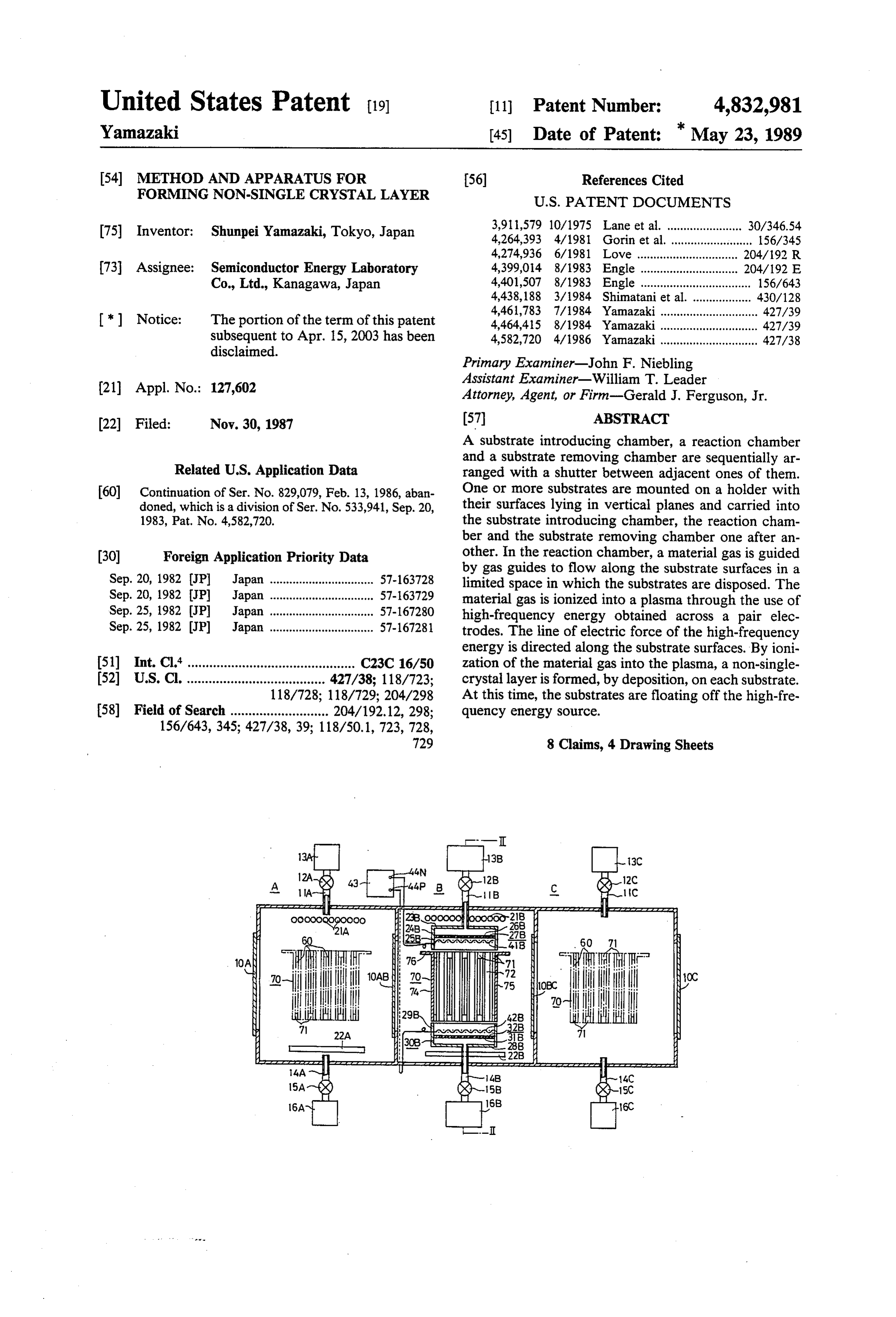
direction of its electric line of force is selected to cross the substrate. On account of this, the non-single-crystal 45 BRIEF DESCRIPTION OF THE DRAWINGS layer may sometimes be damaged due to sputtering by FIG. 1 is a schematic longitudinal sectional view of the excited material gas, i.e. the material gas plasma. an example of the non-single-crystal layer forming ap Furthermore, in the case of using high-frequency paratus according to the present invention, explanatory electrical energy which is obtained across a pair of of an example of the non-single-crystal layer forming electrodes, the material gas is excited in such a state that 50 method of the invention;
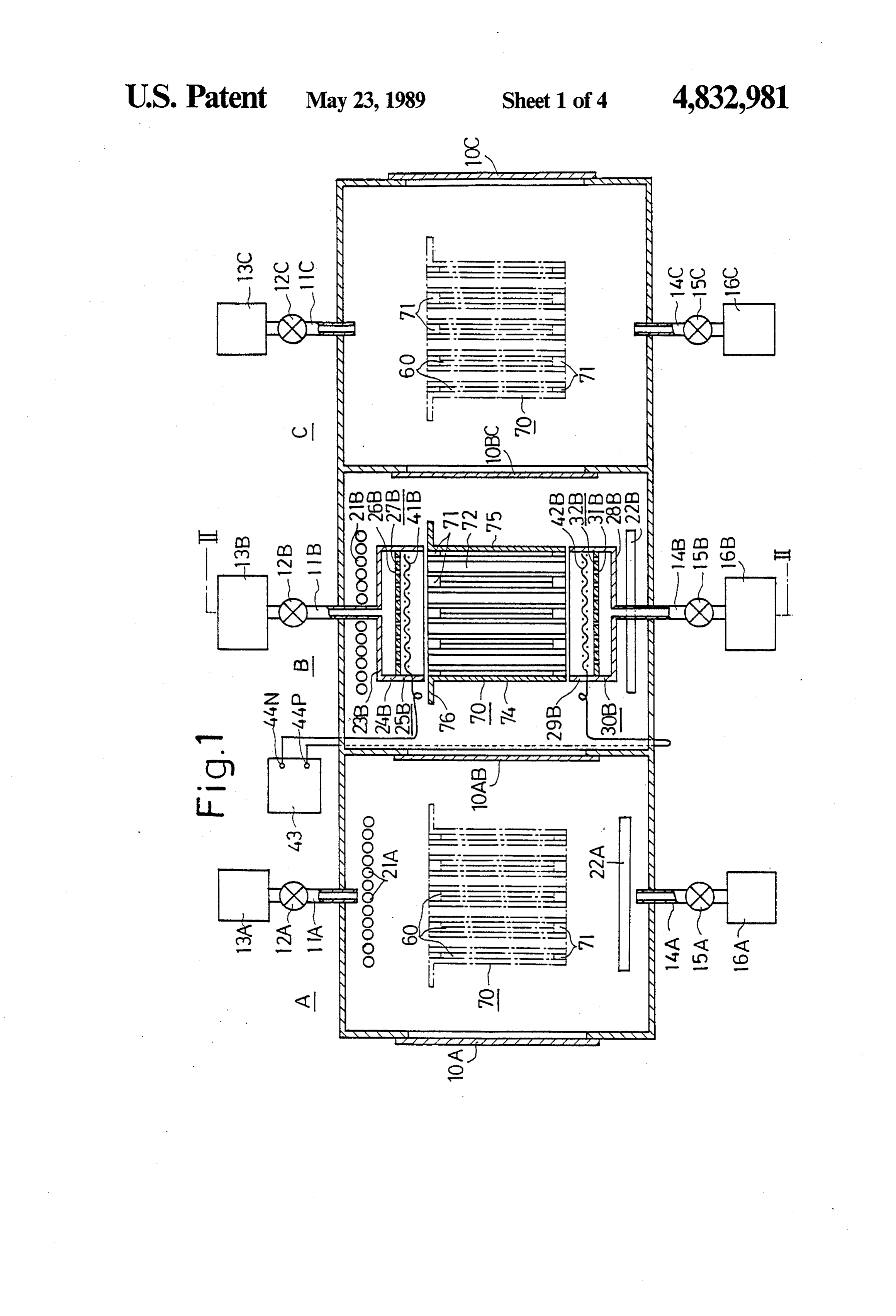
the potential of either one of the electrodes is being FIG. 2 is a sectional view taken on the line II-II in applied to the substrate. With this method, however, FIG. 1;
undesirable flakes formed by the excited material gas FIG. 3 is a schematic longitudinal sectional view, stick to the substrate surface, resulting in the non-single corresponding to FIG. 2, of another example of the crystal layer containing the flakes in quantity. 55 non-single-crystal layer forming apparatus according to A conventional non-single-crystal layer forming ap the present invention, explanatory of another example paratus for the above said method naturally possesses of the non-single-crystal layer forming method of the such defects as mentioned above. invention;
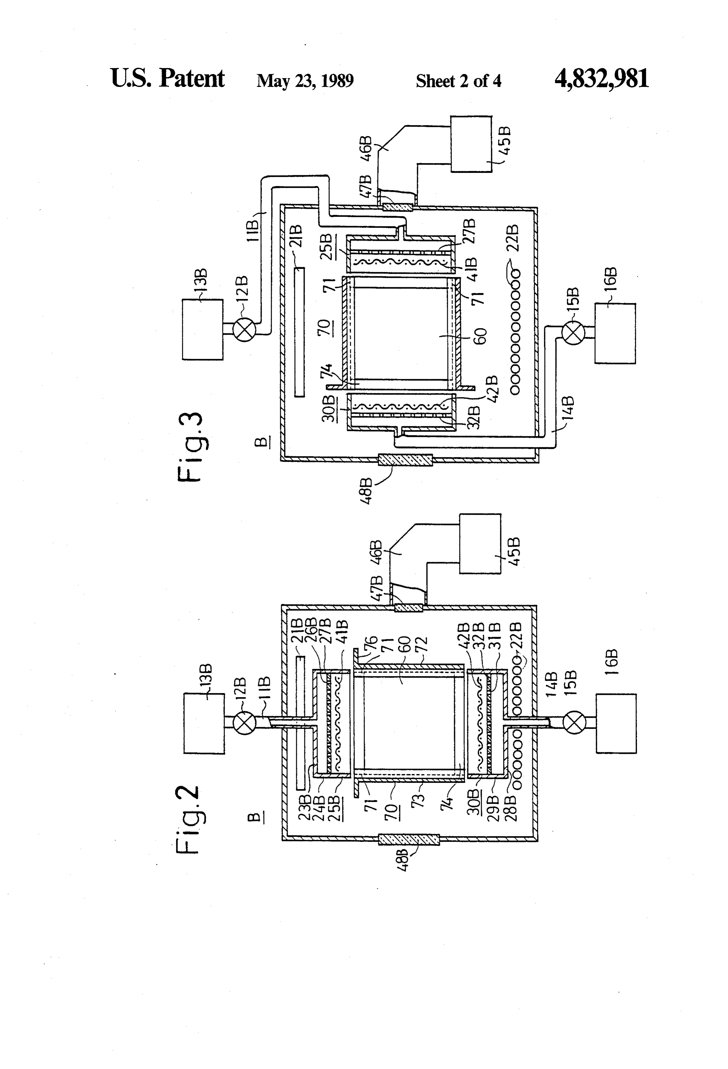
SUMMARY OF THE INVENTION FIGS. 4 and 5 are schematic sectional view respec tively illustrating modified forms of a holder for use in
It is therefore an object of the present invention to the non-single-crystal layer forming method of the pres provide a novel non-single-crystal forming method and ent invention; and apparatus which are free from the above said defects. FIG. 6 is a schematic longitudinal sectional view, In accordance with an aspect of the present inven corresponding to FIG. 1, of another example of the tion, a material gas stream in the reaction chamber is non-single-crystal layer forming apparatus according to directed to the limited space in which a substrate is the present invention, explanatory of another example placed, and is passed over the substrate surface, forming of the non-single-crystal layer forming method of the thereon a non-single-crystal layer. With this method, invention.
Page 7
DESCRIPTION OF THE PREFERRED
red heaters 22B and coaxially with the gas guide 25B in
EMBODIMENTS opposing relation thereto. The gas guide 30B is linked, on the side of the end plate 28B, with the gas exhaust
A description will be given first of the non-single pipe 14B extending from the exhaust pump 16B. In the crystal layer forming apparatus of the present invention. 5 cylindrical body 29B of the gas guide 30B a plate 32B, FIG. 1 illustrates an embodiment of the apparatus which is similar to the aforementioned plate 27B and which has the following arrangement. has a number of through holes 31B, is disposed in a A substrate introducing chamber A, a reaction cham horizontal plane at a distance from the end palte 28B. ber B and a substrate removing chamber C are arranged In the cylindrical body 24B of the gas guide 25B a in this order. 10 mesh-like or perforated-plate-like gas-permeable elec The substrate introducing chamber A is so designed trode 41B is disposed in a horizontal plane on the side of as to communicate with the outside when a shutter 10A the plate 27B. Further, a similar electrode 42B is dis is opened which is provided on the opposite side from posed in a horizontal plane on the side of the plate 32B the reaction chamber B. The substrate introducing in the cylindrical body 29B of the gas guide 30B. chamber A and the reaction chamber B are constructed 15 The electrodes 41B and 42B disposed in the reaction so that they intercommunicate when a shutter 10AB is chamber B are respectively connected to a cathode opened which is provided therebetween. The reaction terminal 44N and an anode terminal 44P of a high-fre chamber B and the substrate removing chamber C are quency power source 43 which is disposed outside the similarly constructed so that they intercommunicate reaction chamber B and provides a high frequency of when a shutter 10BC is opened which is provided there 20 13.56 MHz.
between. The substrate removing chamber C is so Further, as will be seen from FIG. 2, the reaction adapted as to communicate with the outside when a chamber B is connected, on the side of its rear panel, to shutter 10C is opened which is provided on the opposite an ultrahigh frequency power source 45B, which is a side from the reaction chamber B. microwave source or millimeter wave source, through The substrate introducing chamber A is linked with 25 a waveguide 46B and a window 47B which is made in an inert gas source 13A through an inert gas supply pipe the rear panel of the reaction chamber B and which 11A and a gas stream control valve 12A, and is linked inhibits the passage therethrough of gas but permits the with an exhaust pump 16A through a gas exhaust pipe passage therethrough of ultrahigh frequency power. 14A and a gas stream control valve 15A. Incidentally, as will be seen from FIG. 2, the front The reaction chamber B is linked with a material gas 30 panel of the reaction chamber B has made therein an source 13B through a material gas supply pipe 11B and inspection or observation window 48B for observation a gas stream control valve 12B, and is linked with an of the inside thereof. The front panel of each of the exhaust pump 16B through a gas exhaust pipe 14B and substrate introducing chamber A and the substrate re a gas stream control valve 15B. moving chamber C has also made therein a similar ob The substrate removing chamber C is linked with an 35 servation window for observation of the inside thereof, inert gas source 13C through an inert gas supply pipe though not shown.
11C and a gas stream control valve 12C, and is linked The above is a description of the arrangement of one with an exhaust pump 16C through a gas exhaust pipe embodiment of the non-single-crystal layer forming 14C and a gas stream control valve 15C as is the case apparatus.
with the substrate introducing chamber A. 40 Such a non-single-crystal layer forming apparatus is In the substrate introducing chamber A rod-like in used with the non-single-crystal layer forming method frared heaters 21A are arranged in succession in a hori of the present invention.
Zontal plane to extend in the direction perpendicular to Next, a description will be given of the non-single the plane of paper on the side of the top wall of the crystal layer forming method of the present invention. chamber A. On the side of the bottom wall similar infra 45 An example of the non-single-crystal layer forming red heaters 22A are arranged in succession in a horizon method is carried out through the use of the above tal plane to extend in the direction perpendicular to the described apparatus in the following manner: direction of extension of the infrared heaters 21A. Outside the apparatus, a number of substrates 60 are Also in the direction chamber B, infrared heaters 21B premounted on a holder 70 as indicated by the broken and 22B are similarly disposed on the side of the top 50 lines in the reaction chamber B in FIGS. 1 and 2. wall and the side of the bottom wall of the chamber B. The holder 70 has a square tubular body which is On the side of the infrared heaters 21B disposed in the comprised of a pair of plates 72 and 73, each having a reaction chamber Bagas guide 25B, which is formed by number of parallel groove 71 for receiving marginal a cylindrical body 24B made of an insulating material edges of the substrates 60 and another pair of plates 74 and covered at one end with an end plate 23B similarly 55 and 75. The plates 72 and 73 are held in vertical planes made of an insulating material, is disposed in the vertical and in parallel and opposing relation to each other with direction with the end plate 23B on the side of the infra their grooves 71 extending in the vertical direction. The red heaters 21B. The gas guide 25B is linked, on the side plates 74 and 75 are also held in vertical planes and in of the end plate 23B, with the material gas supply pipe parallel and opposing relation to each other. The holder 11.B extending from the material gas source 13B. In the 60 70 has a flange 76 which is formed integrally with the cylindrical body 24B of the gas guide 25B a plate 27B square tubular body to extend outwardly thereof in a made of an insulating material and having a number of horizontal plane.
through holes 26B is disposed in a horizontal plane at a The substrate 60 are received at one of their opposite distance from the end plate 23B. On the side of the marginal edges by the grooves 71 of the plate 72 and at infrared heaters 22B disposed in the reaction chamber B 65 the other marginal edge by the grooves 71 of the plate a similar gas guide 30B, which is formed by a cylindrical 73 so that they may be held by the holder 70 in parallel body 29B closed at one end with an end plate 28B, is and have their surfaces extending in vertical planes. The disposed with the end plate 28B on the side of the infra outermost ones of the substrates 60 on both sides have
Page 8
their backs held in contact with the inner surfaces of the non-single-crystal silicon nitride layer can be formed; plates 74 and 75, respectively, and the other remaining when a gas mixture of a silane gas, nitrogen peroxide substrates 60 are held in back-to-back relation to adja and nitrogen is used, a non-single-crystal silicon oxide cent ones of them. layer can be formed; and when a gas mixture of a mo The holder 70 having mounted thereon the substrates lybdenum chloride gas or tungsten fluoride gas and 60 as described above is brought into the substrate intro silane gas is used, a non-single-crystal molybdenum ducing chamber A, with the shutter 10A temporarily silicide or tungsten silicide layer can be formed. opened, as indicated by the chain lines in FIG. 1. In this When the non-single-crystal layers are formed on the case, the holder 70 is supported by a carrier rod (not substrates 60 in the reaction chamber B, the material gas shown) at the underside of the flange 76 and brought 10 from the material gas supply pipe 11B enters and into the substrate introducing chamber A. The holder spreads between the end plate 23B and the plate 27B 70 thus brought into the chamber A is supported at the having the apertures 26B in the cylindrical body 24B of underside of the flange 76 by a support member (not the gas guide 25B, thence passes through the apertures shown) which is manipulated from the outside of the 26B of the plate 27B and thence flows across the elec substrate introducing chamber A so that the surfaces of 15 the substrates 60 may lie in vertical planes, though not trodecent 41B. Then the material gas flows between adja ones of the substrates 60. Next, the material gas described in detail.
Next, the substrates 60 and the holder 70 are heated 30B, thencetheflows flows into cylindrical body 29B of the gas guide across the electrode 42B, thence by the infrared heaters 21A and 22A provided in the flows through the apertures 31B of the plate 32B, there substrate introducing chamber A and, at the same time, after flowing between the end
gas in the chamber A is discharged by the exhaust pump 32B having the apertures 31B plate 28B and the plate 16A to the outside through the gas exhaust pipe 14A 29B of the gas guide 30B. Next,inthethematerial cylindrical body gas is dis and the gas stream control valve 15A to make the inside of the substrate introducing chamber A vacuous, charged to the outside through the gas exhaust pipe 14B, the gas stream control valve 15B and the exhaust thereby cleansing the substrates 60 and the holder 70. 25 pump 16B.
In this while, gas in the reaction chamber B is ex In the reaction chamber B the material gas flows hausted by the exhaust pump 16B through the gas ex between adjacent haust pipe 14B and the gas stream control valve 15B to defined by the gasones of the substrate 60 in the space guides 25B and 30B as described make the inside of the chamber B vacuous, cleaning it. above. When the material gas flows between adjacent Next, the shutter 10AB between the chambers A and 30
B is temporarily opened and the holder 70, which has ones of the substrates 60, it is limited by the both outer mounted thereon the substrates 60 purified in the cham most ones of the substrates 60 and the plates 72 to 75 of ber A, is brought into the reaction chamber B while the holder 70 from spreading out laterally. The spaces being supported by a carrier rod (not shown) which is defined between the gas guide 25B and the holder 70 inserted from the outside of the substrate introducing 35 and between the holder 70 and the gas guide 30B are chamber A in the same manner as described above. The both very small.
holder 70 thus brought into the reaction chamber B is Accordingly, the material gas in the reaction cham supported by a support member (not shown) so that the ber B flows along the substrate surfaces in the limited substrates 60 may be positioned between the gas guides space in which the substrates 60 are disposed. 25B and 30B, with the substrate surfaces held in vertical This permits the formation of the non-single-crystal planes, as described previously. layers with a high utilization rate of the material gas and Next, the gas in the reaction chamber B is discharged at high rate. Further, flakes are hardly formed on the by the exhaust pump 16B to the outside through the gas inner wall of the reaction chamber Band, consequently, exhaust pipe 14B and the gas stream control valve 15B substantially no flakes fall off the inner wall of the and, at the same time, a material gas is introduced into 45 chamber B. Moreover, even if flakes are formed on that the reaction chamber B from the material gas source part of the holder 70 which is not covered with the 13B through the material gas supply pipe 11B and the substrates 60 and on the interior surface of the gas guide gas stream control valve 12B. Further, high frequency 25B and even if such flakes fall off them, the substrate is applied across the electrodes 41B and 42B from the surfaces are almost free from the bombardment with the high-frequency power source 43. At the same time, 50 flakes because they are held in vertical planes. Accord ultrahigh-frequency power is introduced into the reac ingly, the non-single-crystal layers can be formed with tion chamber B from the ultrahigh-frequency power practically no flakes and pinholes.
source 45B through the waveguide 46B and the win The material gas, when flowing between adjacent dow 47B and, further, the inside of the reaction cham ones of the substrates 60, is excited into a plasma by ber B is heated by the infrared heaters 21B and 22B, by 55 high-frequency electric energy which is obtained across which the material gas introduced into the reaction the electrodes 41B and 42B by high-frequency power chamber B is excited for ionization into a plasma. In this applied thereacross from the high-frequency source 43, way, non-single-crystal layers (not shown) are formed ultrahigh-frequency energy which is created by ul on the substrates 60 in the reaction chamber B. trahigh-frequency power supplied into the reaction In this case, when a silane gas is used as the material chamber B and thermal energy which is radiated from gas, a non-single-crystal silicon layer; when a gas mix the infrared heaters 21B and 22.B. In this case, the elec ture of aluminum chloride and/or triethyl aluminum, trodes 41B and 42B lie in horizontal planes, whereas the hydrogen and/or helium is employed, a non-single substrate surfaces lie in vertical planes. This ensures that crystal aluminum layer can be formed; when a gas mix the line of electric force of the high-frequency electric ture of a carbonyl compound of iron, nickel or cobalt, 65 energy obtained across the electrodes 41B and 42B is hydrogen and/or helium is employed, a non-single directed along the substrate surfaces.
crystal iron, nickel or cobalt layer can be formed; when Therefore, the non-single-crystal layers are not sub a gas mixture of silane and ammonium gases is used, a stantially subjected to sputtering by the excited material
Page 9
gas, and hence they can be formed with practically no strate introducing chamber A into the reaction chamber damages from sputtering. B, is carried out therefrom into the substrate removing Besides, when the material gas is ionized into a chamber C, the inert gas introduced into the substrate plasma, the substrates 60 are not supplied with the po introducing chamber A from the inert gas source 13A tential of either of the electrodes 41B and 42B; namely, 5 through the gas supply pipe 11A and the gas stream they are floating off the high-frequency power source control valve 12A until the pressure in the chamber A 43. This prevents undesirable flakes from sticking to the rises up to the atmospheric pressure or a pressure close non-single-crystal layers. Consequently, the non-single thereto, after which the shutter 10A is opened and a crystal layers can be formed with practically no flakes. second holder 70 carrying new substrates 60 is brought In addition, since the substrates 60 are spaced apart 10 into the substrate introducing chamber A and then the from the electrodes 41B and 42B, the entire area of each supply of the inert gas to the chamber A from the inert substrate surface is positioned in a region in which the gas source 13A is stopped, thereafter holding the inside high-frequency energy developed across the electrodes of the chamber A in a vacuum condition as described 41B and 42B is stable. Accordingly, the non-single-crys previously.
tal layers can each beformed homogeneously and to the 15 Moreover, when the first holder 70 carrying the sub same thickness throughout it. strates 60 with the non-single-crystal layers formed Further, the electrode 41B disposed upstream of the thereon is brought into the substrate removing chamber material gas passage and the electrode 42B disposed C from the reaction chamber B, the second holder 70 downstream of the material gas passage are a cathode placed in the chamber A until then is brought out there and an anode, respectively, so that even if flakes stick to from into the reaction chamber B, with the shutter the gas guides 25B and 30B and the holder 70, the 10AB opened, and then non-single-crystal layers are amount of flakes sticking to the upstream gas guide 25B formed on the substrates mounted on the second holder and the portion of the holder on the upstream side is far 70 as described previously. And, in the period in which smaller than the amount of flakes sticking to the down the non-single-crystal layers are thus formed on the stream gas guide 30B and the portion of the holder 70 25 substrate 60 mounted on the holder 70, a third holder 70 on the downstream side. Therefore, the non-single-crys is carried into the substrate introducing chamber A in tal layer can be formed with practically no flakes. the same way as described previously. After forming the non-single-crystal layers on the Furthermore, after the first holder 70 carrying the substrates 60 in the reaction chamber B as described substrates 60 with the non-single-crystal layers formed above, the supply of the material gas from the material 30 thereon is brought out of the substrate removing cham gas source 13B to the reaction chamber B is stopped, ber C and after the inside of the chamber C is made holding the inside of the reaction chamber B vacuous. vacuous, the second holder 70 is carried into the cham On the other hand, while the non-single-crystal layers ber C and, at the same time, the third holder 70 is car are being formed on the substrates 60 in the reaction ried out of the chamber A into the chamber B. chamber B as described above, gas in the substrate re 35 In the manner described above, the substrates 60 moving chamber C is discharged by the exhaust pump having formed thereon the non-single-crystal layers are 16C to the outside through the gas exhaust pipe 14C and continuously obtained.
the gas stream control valve 15C to make the inside of The above is a description of an example of each of the substrate removing chamber C, thereby purifying it. the non-single-crystal layer forming method and appa Next, after the formation of the non-single-crystal 40 ratus of the present invention. Next, a description will layers on the substrates 60 in the reaction chamber B, be given of modifications and variations of this inven the shutter 10BC between the chambers B and C is tion method and apparatus.
opened and the holder 70 which has mounted thereon The reaction chamber B of the apparatus described the substrates 60, which have formed thereon the non previously in connection with FIGS. 1 and 2 can be single-crystal layers, is brought into the substrate re 45 modified as follows: That is, the gas guides 25B and 30B moving chamber C as indicated by the chain line in in the chamber B can also be disposed on the sides of the FIG. 1. In this case, the holder 70 is supported by a rear and front walls of the chamber B instead of being carrier rod (not shown) inserted from the outside of the disposed on the sides of the top and bottom walls chamber C and is moved into the chamber C in the same thereofas shown in FIG. 3. Needless to say, in this case, manner as referred to previously. Further, the holder 70 50 the apertured plate 27B and the electrode 41B are dis thus brought into the substrate removing chamber C is posed in the gas guide 25B, and the apertured plate 32B supported by a support member (not shown) in the same and the electrode 42B are placed in the gas guide 30B as manner as described previously. is the case with FIGS. 1 and 2. Next, the inert gas is introduced into the substrate Further, when such apparatus as shown in FIG. 3 is removing chamber C from the inert gas source 13C 55 used, the non-single-crystal layer forming method is through the inert gas supply pipe 11C and the gas modified correspondingly as follows:
stream control valve 12C so that the pressure in the While in the foregoing example the holder 70 is de chamber C rises up to the atmospheric pressure or a signed so that when it is transferred into the chambers pressure close thereto. A, B and C one after another, its grooves 71 extend in Next, the shutter 10C is opened and the holder 70 is 60 the vertical direction and, consequently, the substrates brought out of the chamber C, and then the supply of 60 mounted on the holder 70 lie in the vertical planes, the inert gas from the inert gas source 13C to the sub the holder 70 is adapted so that its grooves 71 extend in strate removing chamber C is stopped. Finally, the the horizontal direction and so that the substrates 60 lie substrates 60 having formed thereon the non-single in vertical planes.
crystal layers are dismounted from the holder 70. 65 In such a case, though not described in detail, the In practice, in the period during which the holder 70 relation between the substrates 60 and the material gas (hereinafter referred to as the first holder 70) having flow and the relation between the substrates 60 and the mounted thereon the substrates, carried out of the sub electrodes 41B and 42B in the reaction chamber B are
Page 10
the same as those in the case of FIGS. 1 and 2, so that tion chambers E, F and G, it is possible to form on each non-single-crystal layers can be formed on the sub substrate 60 three non-single-crystal layers in the form strates 60 with the same excellent features as described of a laminate layer in the reaction chambers E, F and G previously in respect of FIGS. 1 and 2. one after another in the same manner as described previ With the non-single-crystal layer forming method of ously. Accordingly, it is possible to fabricate on each the present invention described in the foregoing, the substrate a photoelectric conversion device which has a substrates 60 are transferred through the chambers A, B Ptype non-single-crystal semiconductor layer, an I type and C while being held with the substrate surfaces in non-single-crystal semiconductor layer and an N type vertical planes. non-single-crystal semiconductor layer formed in suc However, though not described in detail, even if the 10 cession and serves as a solar cell. substrates 60 are mounted on the holder 70 with the Although in the foregoing the high-frequency en substrate surface aslant as shown in FIGS. 4 and 5, ergy, the ultrahigh-frequency energy and the thermal when the inclination angle of the substrate surface to energy are employed for excitation of the material gas, the vertical plane is sufficiently small, non-single-crystal the ultrahigh-frequency energy and the thermal energy layers can be formed on the substrates 60 in the same 15 need not always used, and photo energy can also be manner as described previously. employed in place of one or more of the high-fre Besides, although in the foregoing one non-single quency, the ultrahigh frequency and the thermal en crystal layer is formed on each substrate 60 in the reac ergy.
tion chamber B, it is also possible to form a plurality of It will be apparent that many modifications and varia non-single-crystal layers of different kinds on each sub 20 tions may be effected without departing from the scope strate 60 by introducing different material gases one of the novel concepts of the present invention. after another into the reaction chamber B while the What is claimed is:
substrates 60 are held therein. 1. An apparatus for forming at least one non-single Moreover, while in the foregoing the non-single crystal layer on a plurality of substrates comprising: crystal layer forming apparatus has one reaction cham 25 a substrate introducing chamber;
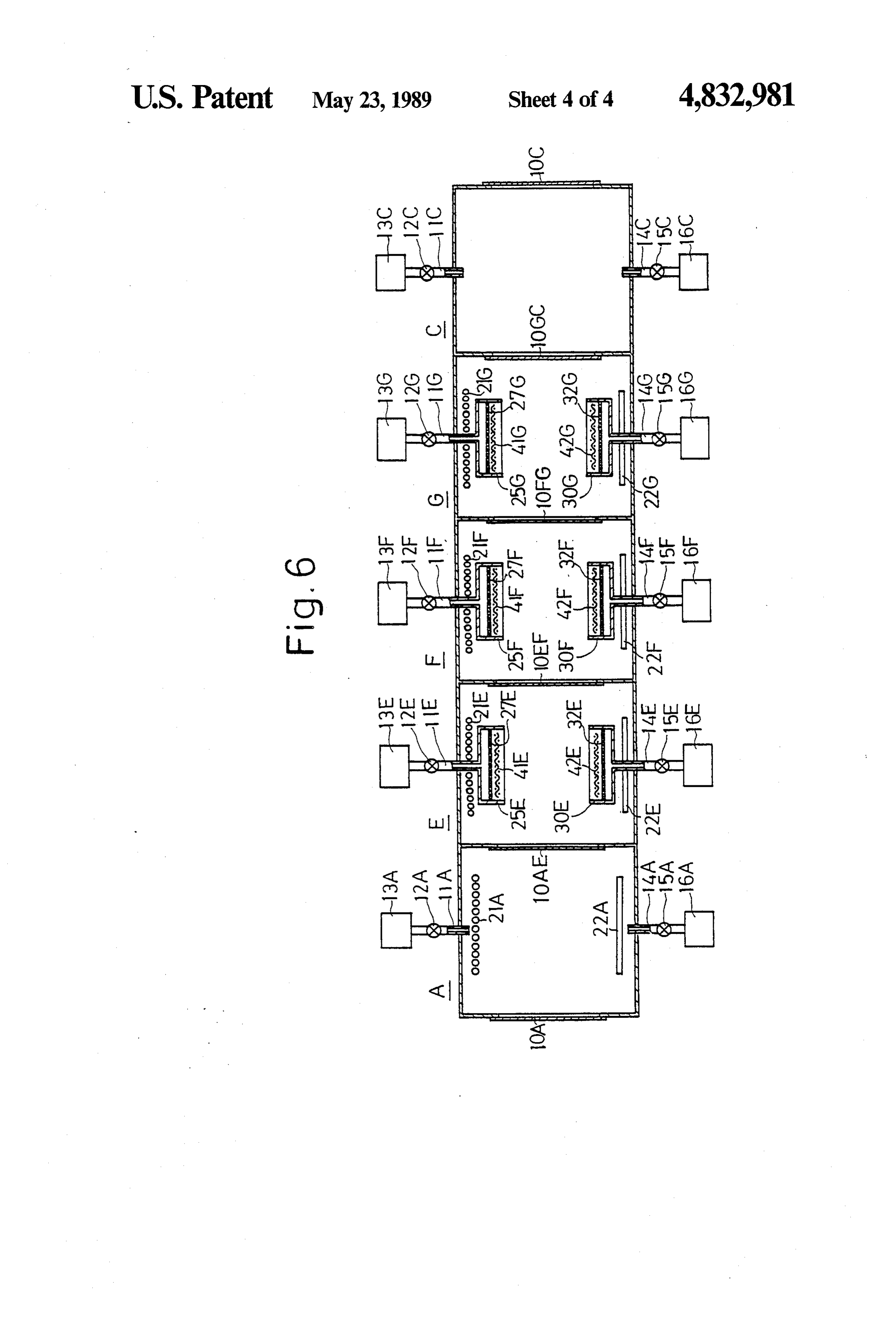
ber B, plural, for instance, three reaction chambers E, F a tubular substrate holder for holding a plurality of and G, similar to the reaction chamber B, may also be substrates with their surfaces lying in vertical arranged successively between the substrate introduc planes or planes close thereto; ing chamber A and the substrate removing chamber C means for introducing said substrate holder into said through shutters 10AE, 10EF, 10FG and 10GC which 30 substrate introducing chamber; are similar to the shutters 10AB and 10BC as shown in means for cleaning the substrates and the substrate FIG. 6. In this case, a material gas source 13E is linked holder while in the substrate introducing chamber, with the reaction chamber E through a material gas by discharging gas in the substrate introducing supply pipe 11E and a gas stream control valve 12E, chamber through use of an exhaust pump; and an exhaust pump 16E is linked with the reaction 35 at least one reaction chamber;
chamber E through a gas exhaust pipe 14E and a gas means for transferring the cleaned substrate holder stream control valve 15E. A material gas source 13F is and substrates to the reaction chamber; linked with the reaction chamber F through a material means for depositing non-single-crystal layers respec gas supply pipe 11F and a gas stream control valve 12F, tively on said substrates through a CVD process by and an exhaust pump 16F is linked with the reaction supplying a stream of a material gas into the tubular chamber F through a gas exhaust pipe 14F and a gas substrate holder while in said reaction chamber, the stream control valve 15F. A material gas source 13G is depositing means being provided with means for linked with the reaction chamber G through a material heating said substrate holder and said substrates gas supply pipe 11G and a gas stream control valve from the outside of the substrate holder; 12G, and an exhaust pump 16G is linked with the reac 45 a substrate removing chamber; and tion chamber G through a gas exhaust pipe 14G and a means for transferring said sustrate holder and the gas stream control valve 15G. coated substrates to the substrate removing cham Further, in the reaction chamber E are disposed infra ber, red heaters 21E and 22E similar to the aforementioned wherein the depositing means is provided with means ones 21B and 22B, gas guides 25E and 30E similar to the 50 for introducing the material gas into the reaction aforementioned ones 25B and 30B, plates 27E and 32E chamber, first and second gas guide means for similar to the aforementioned ones 27B and 32B, and guiding the material gas to pass it along the sub electrodes 41E and 42E similar to the aforementioned strate surfaces, means for exhausting gas from the ones 41B and 42B. In the reaction chamber F are dis reaction chamber and means for exciting the mate posed infrared heaters 21F and 22F similar to the afore 55 rial gas, wherein the material gas exciting means is mentioned ones 21B and 22B, gas guides 25F and 30F provided with first and second electrodes for ob similar to the aforementioned ones 25B and 30B plates taining high-frequency electric energy, and 27F and 32F similar to the aforementioned ones 27B wherein the first and second electrodes are dis and 32B, and electrodes 41F and 42F similar to the posed so that the line of electric force of the high aforementioned ones 41B and 42B. In the reaction frequency electric energy may extend along the chamber G are disposed infrared heaters 21G and 22G substrate surfaces, and wherein the first and second similar to the aforementioned ones 21B and 22B, gas electrodes are disposed as a cathode and an anode guides 25G and 30G similar to the aforementioned ones upstream and downstream of a material gas pas 25B and 30B, plates 27G and 32G similar to the afore sage, respectively, and wherein the first and second mentioned ones 27B and 32B, and electrodes 41G and 65 electrodes have the property of permitting the 42G similar to the aforementioned ones 41B and 42B. passage therethrough of the material gas, and are With the use of the non-single-crystal layer forming disposed in the first and second gas guide means, apparatus shown in FIG. 6, since it has the three reac respectively.
Page 11
2. Non-single-crystal layer forming apparatus accord 6. A non-single-crystal layer forming method accord ing to claim 1, wherein the material gas exciting means ing to claim 3, wherein the material gas is excited by is provided with means for supplying ultrahigh-fre ionization into a plasma through use of high-frequency quency electric energy into the reaction chamber. energy having its line of electric force extending along 3. A method for forming at least one non-single-crys the substrate surfaces and ultrahigh-frequency electric tal layer on a plurality of substrates, comprising the energy.
steps of: 7. A method for forming at least one non-single-crys providing a substrate introducing chamber; tal layer on a plurality of substrates, comprising the providing a tubular substrate holder for holding said 10 steps of:
providing a substrate introducing chamber;
plurality of substrates with their surfaces lying in providing a tubular substrate holder for holding said vertical planes or planes close thereto; plurality of substrates with their surfaces lying in introducing said substrate holder into said substrate vertical planes or planes close thereto; introducing chamber; introducing said substrate holder onto said substrate cleaning the substrates and the substrate holder while 15 introducing chamber;
in the substrate introducing chamber, by discharg cleaning the substrates and the substrate holder while ing gas in the substrate introducing chamber in the substrate introducing chamber, by discharg through use of an exhaust pump; ing gas in the substrate introducing chamber providing at least one reaction chamber; through use of an exhaust pump; transferring the cleaned substrate holder and sub 20 providing at least one reaction chamber; strates to the reaction chamber; transferring the cleaned substrate holder and sub depositing non-single-crystal layers respectively on strates to the reaction chamber; said substrates through a CVD process by supply depositing non-single-crystal layers respectively on ing a stream of a material gas into the tubular sub said substrates through a CVD process by supply strate holder while in said reaction chamber, 25 ing a stream of a material gas into the tubular sub wherein the substrate holder and the substrates are strate holder while in said reaction chamber, heated from the outside of the substrate holder; wherein the substrate holder and the substrates are providing a substrate removing chamber; heated from the outside of the substrate holder; transferring said substrate holder and the coated sub providing a substrate removing chamber; strates to the substrate removing chamber, 30 transferring said substrate holder and the coated sub wherein the material gas is guided by first and second strates to the substrate removing chamber, gas guide means provided upstream and down wherein said material gas is guided by first and sec stream of a gas passage, respectively, so that the ond gas guide means provided upstream and down stream of the material gas passes along the sub stream of a gas passage, so that when said tubular strate surfaces in the limited space in which the 35 substrate holder is transferred to the reaction substrates are placed, wherein the substrates are chamber for depositing, said tubular substrate disposed at predetermined intervals, and wherein holder is positioned within said gas passage be the stream of the material gas passing along the tween said first and second gas guide means so that surface of each of the substrates is prevented by said first gas guide means, said tubular substrate both outermost ones of them from spreading later holder and said second gas guide means together ally; substantially define a flow path of said material gas wherein the material gas is ionized into a plasma for through said reaction chamber; excitation by high-frequency electric energy hav wherein the material gas is ionized into a plasma for ing its line of electric force extending along the 45 excitation by high-frequency electric energy hav substrate surfaces; ing its line of electric force extending along the wherein the high-frequency electric energy is ob substrate surfaces;
tained across first and second electrodes disposed wherein the high-frequency electric energy is ob in the reaction chamber, and wherein the material tained across first and second electrodes disposed gas is ionized into a plasma in a state in which the 50 in the reaction chamber, and wherein the material substrates are disposed between the first and sec gas is ionized into a plasma in a state in which the ond electrodes and are not supplied with the poten substrates are disposed between the first and sec tial of either of the first and second electrodes; ond electrodes and are not supplied with the poten tial of either of the first and second electrodes;
and wherein the material gas is ionized into a plasma and wherein the material gas is ionized into a plasma in a state in which the first electrode is disposed in 55 in a state in which the first electrode is disposed as said first gas guide means as a cathode upstream of a cathode upstream of the material gas passage and the material gas passage and the second electrode is the second electrode is disposed as an anode down disposed in said second gas guide means as an stream of the material gas passage. anode downstream of the material gas passage. 8. A non-single-crystal layer forming method accord 4. A non-single-crystal forming method according to 60 ing to claim 7, wherein the material gas is ionized into a claim 3, wherein the material gas is excited by photo plasma in a state in which electrodes permitting the energy. passage therethrough of the material gas are disposed as 5. A non-single-crystal layer forming method accord the first and second electrodes in the first and second ing to claim 3, wherein the material gas is excited by gas guide means.
both electric and photo energy. 65 :
Provenance
- Collection
- Cited prior art
- Original PDF
- patentimages.storage.googleapis.com →
- Filed
- 1987-11-30
- Pages
- 11
- Method
- pdftotext (the PDF's own text layer) + pdftoppm 300dpi page scans
- Source
- Google Patents bibliographic record
- Granted
- 1989-05-23
- Inventors
- Shunpei Yamazaki; Semiconductor Energy Laboratory Co Ltd
- Transcribed from
- patentimages.storage.googleapis.com →