patent · US4511756
Amorphous silicon solar cells and a method of producing the same
16 April 1985
Page 1 — bibliographic record
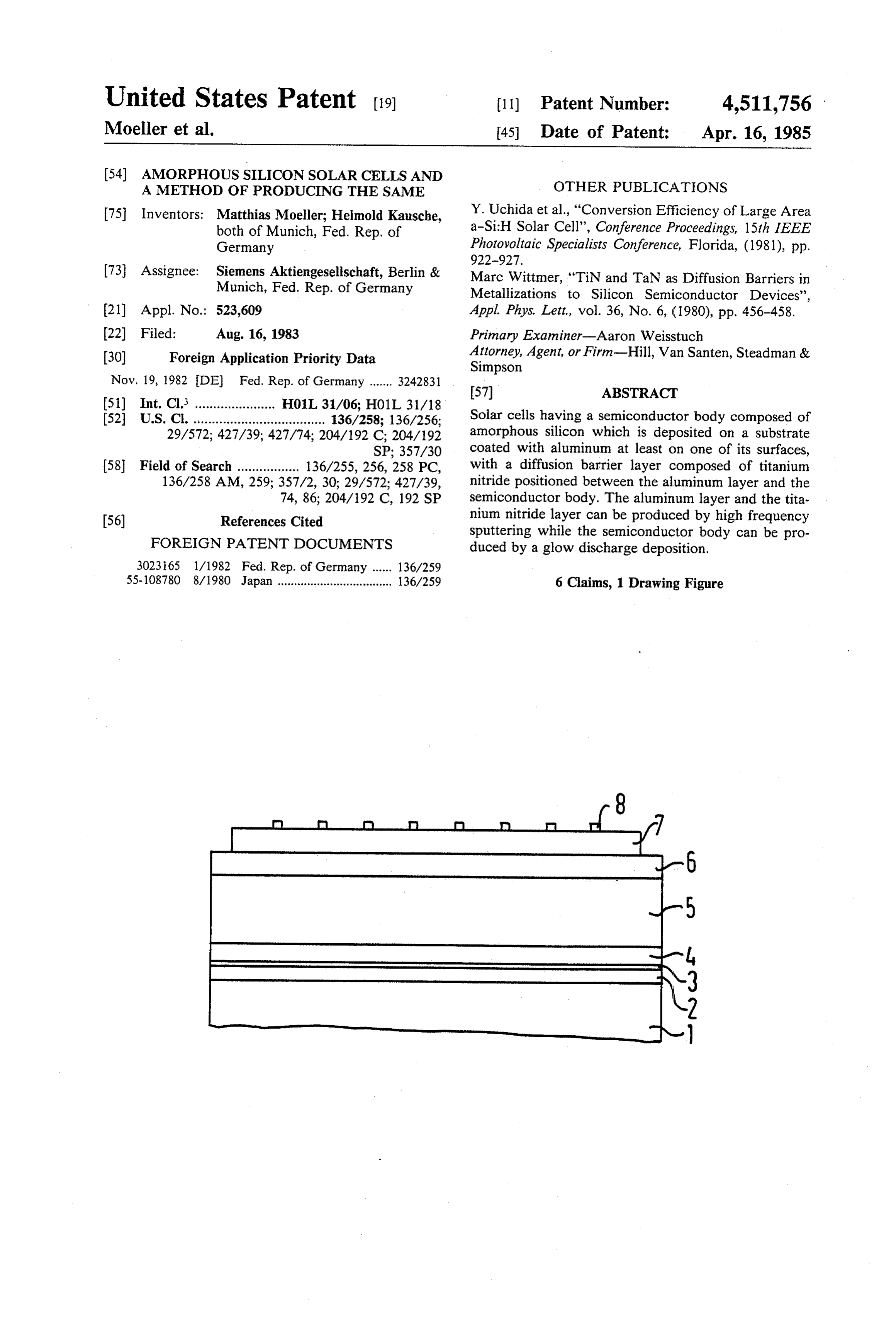
United States Patent (19) 11) Patent Number: 4,511,756 Moeller et al. 45 Date of Patent: Apr. 16, 1985 (54) AMORPHOUS SILICONSOLAR CELLS AND OTHER PUBLICATIONS
A METHOD OF PRODUCING THE SAME
75) Inventors: Matthias Moeller; Helmold Kausche, Y. Uchida et al., "Conversion Efficiency of Large Area both of Munich, Fed. Rep. of a-Si:H Solar Cell', Conference Proceedings, 15th IEEE Germany Photovoltaic Specialists Conference, Florida, (1981), pp.
73 Assignee: Siemens Aktiengesellschaft, Berlin & Marc Wittmer, "TiN and TaN as Diffusion Barriers in Munich, Fed. Rep. of Germany Metallizations to Silicon Semiconductor Devices', (2) Appl. No.: 523,609 Appl. Phys. Lett., vol. 36, No. 6, (1980), pp. 456-458. 22 Filed: Aug. 16, 1983 Primary Examiner-Aaron Weisstuch (30) Foreign Application Priority Data Attorney, Agent, or Firm-Hill, Van Santen, Steadman & Simpson
Nov. 19, 1982 IDE Fed. Rep. of Germany ....... 3242831
52 U.S. Cl. .......... who wa w w 48 a 4 w w P wo 136/258; 136/256; Solar cells having a semiconductor body composed of 29/572; 427/39; 427/74; 204/192 C; 204/192 amorphous silicon which is deposited on a substrate SP; 357/30 coated with aluminum at least on one of its surfaces, 58) Field of Search ................. 136/255, 256, 258 PC, with a diffusion barrier layer composed of titanium 136/258 AM, 259; 357/2, 30; 29/572; 427/39, nitride positioned between the aluminum layer and the 74, 86; 204/192 C, 192 SP semiconductor body. The aluminum layer and the tita (56) References Cited nium nitride layer can be produced by high frequency sputtering while the semiconductor body can be pro
FOREIGN PATENT DOCUMENTS duced by a glow discharge deposition.
55-108780 8/1980 Japan ................................... 136/259 6 Claims, 1 Drawing Figure
Page 2
Drawing sheet — no readable text.
Page 3
that the crystalline size of titanium nitride is relatively
AMORPHOUS SILICON SOLAR CELLS AND A small, i.e., a titanium nitride layer is mirror smooth. METHOD OF PRODUCING THE SAME The surface resistance of a titanium nitride layer hav ing a thickness in the range of about 0.1 through 0.5 nm
BACKGROUND OF THE INVENTION 5 and preferably a thickness of about 0.2 nm, is about 200 1. Field of the Invention Ohm. This value is about 10 times higher than the resis The invention relates to solar cells and somewhat tance of a pure titanium layer, presumably being related more particularly to solar cells having a semiconductor to theofnitrogen incorporation. Nevertheless, the resis body formed of amorphous silicon and which is applied O tance a titanium nitride layer is low enough so as not to have a measurable effect as a series resistance in the to a substrate having a metal layer at least on one sur cell face thereof and functioning as a back contact as well as mm)function, cells on as was documented by producing small (6 pure titanium nitride layers in comparison a method of producing such solar cells. to similar sized cells produced on (low resistant) 2. Prior Art
The formation of solar cells comprised of amorphous 15 chrome-nickel
In further layers.
accord with the principles of the invention, silicon (sometimes referred to as a-Si) on insulating, but a titanium nitride layer is produced by high frequency not necessarily transparent, substrates, such as glass, sputtering, with the use of a target consisting of titanium ceramic, or Kapton (a trade name for a commercially in an enclosed gas atmosphere available polyimide film), is particularly significant be that a titanium nitride layer of a containing select nitrogen so thickness is gen cause series-interconnected solar cells can be readily 20 erated on a suitable substrate body, such as an aluminum fabricated on such a substrate by a simple mask tech layer positioned on a glass body. Subsequently, an nique. In order to achieve this, a metal layer with a amorphous silicon semiconductor body is deposited relatively low surface resistance (approximately 50 m onto the titanium nitride layer by thermal decomposi Ohm with a 50 cm2 cell size) must first be applied to the tion of a gaseous compound containing silicon substrate as a back contact. 25 therein-to which select dopant compounds can be It is known from the Conference Proceedings of the added under given conditions-under the influence of a Fifteenth IEEE Photovoltaic Specialist Conference, Flor glow discharge plasma. In an exemplary sputtering ida (1981) pages 922-927, especially FIG. 1, to utilize set-up, an argon gas pressure of 3X 10² Torr and a special steel discs as the substrate in producing a-Sisolar nitrogen gas pressure of 0.2X 10⁻² Torr, with a power cells. 30 of 3 W/cm2 were utilized. Further detail of such a set However, aluminum would be particularly well up can be derived from an article by M. Wittmer in suited as a back contact material because of its high Appl. Phys. Lett, Vol. 36, No. 6, Mar. 15, 1980, pages conductivity and economical price. Decisive, with pro 456-458.
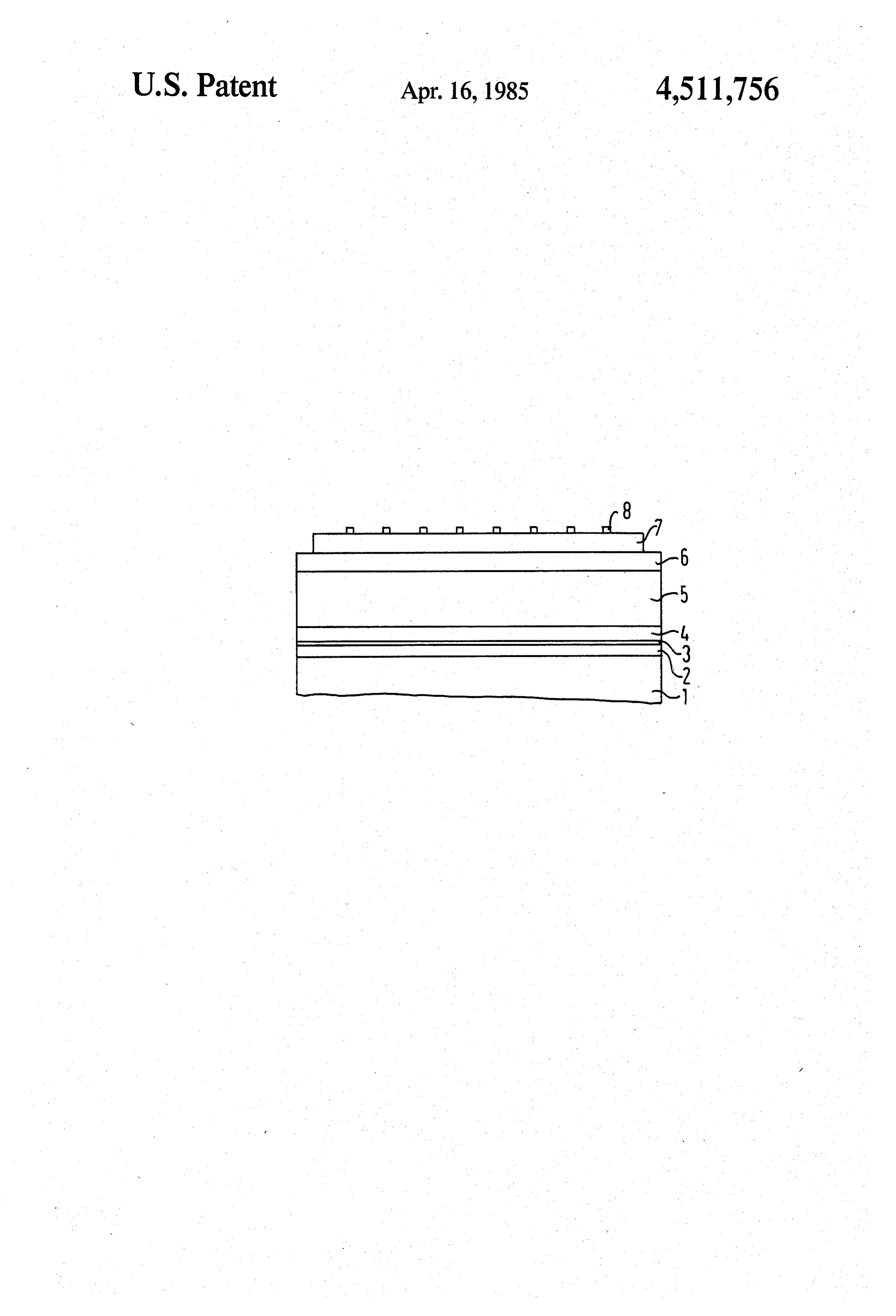
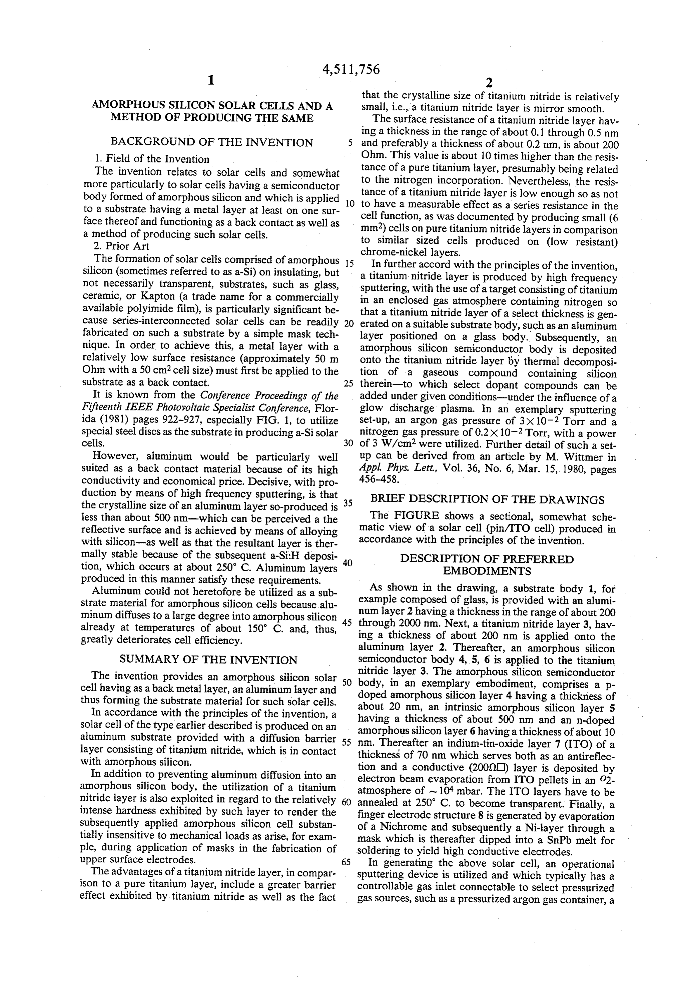
duction by means of high frequency sputtering, is that 35 BRIEF DESCRIPTION OF THE DRAWINGS the crystalline size of an aluminum layerso-produced is less than about 500 nm-which can be perceived a the The FIGURE shows a sectional, somewhat sche reflective surface and is achieved by means of alloying matic view of a solar cell (pin/ITO cell) produced in with silicon-as well as that the resultant layer is ther accordance with the principles of the invention. mally stable because of the subsequent a-Si-H deposi 40 DESCRIPTION OF PREFERRED tion, which occurs at about 250 C. Aluminum layers EMBODIMENTS produced in this manner satisfy these requirements.
Aluminum could not heretofore be utilized as a sub As shown in the drawing, a substrate body 1, for strate material for amorphous silicon cells because alu example composed of glass, is provided with an alumi minum diffuses to a large degree into amorphous silicon 45 num layer 2 having a thickness in the range of about 200 already at temperatures of about 150° C. and, thus, through 2000 nm. Next, a titanium nitride layer 3, hav greatly deteriorates cell efficiency. ing a thickness of about 200 nm is applied onto the aluminum layer 2. Thereafter, an amorphous silicon
SUMMARY OF THE INVENTION semiconductor body 4, 5, 6 is applied to the titanium The invention provides an amorphous silicon solar 50 body, nitride layer 3. The amorphous silicon semiconductor cell having as a back metal layer, an aluminum layer and doped in an exemplary embodiment, comprises a p amorphous silicon layer 4 having a thickness of thus forming the substrate material for such solar cells. about 20 nm, an intrinsic amorphous silicon layer 5 In accordance with the principles of the invention, a solar cell of the type earlier described is produced on an having a thickness of about 500 nm and an n-doped amorphous silicon layer 6 having a thickness of about 10 aluminum substrate provided with a diffusion barrier 55 nm. Thereafter layer consisting of titanium nitride, which is in contact thickness of 70 an nm indium-tin-oxide layer 7 (ITO) of a which serves both as an antireflec with amorphous silicon. tion and a conductive (2000) layer is deposited by In addition to preventing aluminum diffusion into an electron beam evaporation from ITO pellets in an O2 amorphous silicon body, the utilization of a titanium atmosphere of ~ 10 mbar. The ITO layers have to be nitride layer is also exploited in regard to the relatively 60 annealed at 250 C. to become transparent. Finally, a intense hardness exhibited by such layer to render the finger electrode structure 8 is generated by evaporation subsequently applied amorphous silicon cell substan of a Nichrome and subsequently a Ni-layer through a tially insensitive to mechanical loads as arise, for exam mask which is thereafter dipped into a SnPb melt for ple, during application of masks in the fabrication of soldering to yield high conductive electrodes. upper surface electrodes. 65 In generating the above solar cell, an operational The advantages of a titanium nitride layer, in compar sputtering device is utilized and which typically has a ison to a pure titanium layer, include a greater barrier controllable gas inlet connectable to select pressurized effect exhibited by titanium nitride as well as the fact gas sources, such as a pressurized argon gas container, a
Page 4
pressurized nitrogen gas container, a pressurized dopant limiting of the present invention, excepting as it is set compound container, a pressurized silicon-containing forth and defined in the hereto-appended claims. gaseous compound, etc. In addition, the sputtering de What we claim as our invention: vice is controllably connected to a suitable high fre 1. In a solar cell having a semiconductor body com quency energy source. In operation, for example, an 5 posed essentially of amorphous silicon applied to a sub aluminum target into which silicon is alloyed by 1% is strate having at least one surface thereof comprised of a positioned within the sputtering device, along with an metal layer functioning as a back contact, the improve appropriately spaced substrate heated to 200 C. and ment which comprises employing as said metal layer argon is fed into the sputtering space at a pressure of 1. O one which is composed of aluminum and which further 102 mb (millibar), while high frequency energy is nium nitridea diffusion comprises barrier layer composed of tita directed at the 8" target so that relatively small size said semiconductor body.between said metal layer and positioned aluminum crystals (on the order of about 50 nm) are 2. A solar cell as defined in claim 1, wherein said deposited on a substrate with a rate of about 25 nm/min, aluminum until a desired layer of thickness, generally about 200 15 to 2000 nm.layer has a thickness in the range of about 200 through 2000 nm is attained. The aluminum target is 3. A solar cell as defined in claim 1, wherein said then removed or appropriately masked while a titanium titanium nitride layer has a thickness in the range of target is inserted or uncovered. The gas atmosphere about 0.1 to 0.5 nm and exhibits a surface resistance of within the sputtering space is adjusted so that an argon about 200 Ohms.
gas pressure of about 4x10 -2mb (millibar) and a nitro 20 4. A solar cell as defined in claim 3, wherein said gen gas pressure of about 3X 10 3 mb are present, titanium nitride layer has a thickness of about 0.2 nm. while the high frequency power is adjusted to about 3 5. A method of producing a solar cell having a semi W/cm2 so that a relatively thin titanium nitride layer is conductor body composed essentially of amorphous generated on the aluminum layer positioned on the silicon applied to a substrate having at least at one sur substrate body. Subsequently, the targets are removed 25 face thereof comprised of an aluminum layer function or masked and a thermally-decomposable silicon-yield ing as a back contact and further having a diffusion ing gaseous compound such as monosilane or disilane, barrier layer composed of titanium nitride positioned along with about 1% of gaseous dopant-yielding com between said aluminum layer and said semiconductor pounds like diborane or phosphine to produce the n- or 30 body, said method comprising the steps of: m-type layer, are fed into the reaction space. The gas applying said aluminum layer onto a substrate by high pressure is chosen to be about 0.2 mb and therf-power frequency sputtering;
adjusted to about 10 mW/cm2 so that a glow discharge generating a titanium nitride layer onto said alumi plasma occurs and the gaseous compounds thermally num layer by high frequency sputtering with the decompose under the influence of the glow discharge use of a target composed of titanium in a gas atmo sphere containing nitrogen; and plasma. So as to deposit amorphous silicon on the tita 35 depositing nium nitride layer. As indicated above, the amorphous an amorphous semiconductor body onto silicon layer so-deposited can be either p-doped, n the titanium nitride layer by thermally decompos doped or intrinsic.
ing a gaseous compound containing silicon to
As is apparent from the foregoing specification, the 40 which selected dopant compounds are added under present invention is susceptible of being embodied with given conditions under the influence of a glow discharge plasma.
various alterations and modifications which may differ 6. A method as defined in claim 5 wherein, during particularly from those that have been described in the generation of said titanium nitride layer, an argon gas preceding specification and description. For this reason, pressure of about 4X 10.2 mb and a nitrogen gas pres it is to be fully understood that all of the foregoing is 45 sure of about 3X 10⁻³ mb are utilized with a high fre intended to be merely illustrative and is not to be con quency power of about 3 W/cm2.
strued or interpreted as being restrictive or otherwise : k k s k
Provenance
- Collection
- Cited prior art
- Original PDF
- patentimages.storage.googleapis.com →
- Filed
- 1983-08-16
- Pages
- 4
- Method
- pdftotext (the PDF's own text layer) + pdftoppm 300dpi page scans
- Source
- Google Patents bibliographic record
- Granted
- 1985-04-16
- Inventors
- Matthias Moeller; Helmold Kausche; Siemens AG
- Transcribed from
- patentimages.storage.googleapis.com →