patent · US4365106
Efficient method and apparatus for converting solar energy to electrical energy
21 December 1982
Page 1 — bibliographic record
United States Patent (19) (11) 4,365,106 Pulwari (45) Dec. 21, 1982 54) EFFICIENT METHOD AND APPARATUS 3,769,096 10/1973 Ashkin et al. ....................... 136/213 FOR CONVERTING SOLAR ENERGY TO 4,110,616 8/1978 Porter et al. ........................ 250/332 ELECTRICAL ENERGY 4,147,562 4/1979 Chiang et al. ....................... 136/213 4,250,384 2/1981 Pulvari............................ 136/206 X 76 Inventor: Charles F. Pulvari, 2014 Taylor St.,
NE., Washington, D.C. 20018 Primary Examiner-Leland A. Sebastian
Attorney, Agent, or Firm-Jim Zegeer
Notice: The portion of the term of this patent subsequent to Feb. 10, 1998, has been (57) ABSTRACT disclaimed. A very thin insulator having a dipole structure such as (21) Appl. No.: 127,171 a dielectric material having ferroelectric, pyroelectric 22 Filed: Mar. 4, 1980 and or thermodielectric properties, is used as the insula tor insulating an electrode of an electrode pair from a
Related U.S. Application Data semiconductor body sandwiched between said elec trode pair forming a MIS structure. Radiation and solar (63) Continuation-in-part of Ser. No. 69,477, Aug. 24, 1979, energy conversion systems based on establishment of an Pat. No. 4,250,384. inversion layer by the thermally released bound charges (51) Int. Cl'.............................................. H01J 35/00 of a polarizable dielectric layer or an electret and irra 52) U.S. C. .................................... 136/206; 136/213; dation of the semiconductor to separate the electron 136/254; 322/2 R; 357/30 . hole pairs and subsequent collection of mobile carriers.
58) Field of Search ............... 136/206, 213, 214, 254; Since there is no metalurgical junction, the generated 250/330, 338; 307/401; 322/2 R; 357/30 carriers are not junction limited therefore the generated (56) References Cited voltage could be higher than in an ordinary junction solar cell and could also be, an alternating current volt
3,243,687 3/1966 Hoh ................................. 136/213 X 3,256,435 7/1966 Astheimer ....................... 136/213 X 15 Claims, 5 Drawing Figures
(TRANSPARENT FINGER
I5 ELECTRODES)
CONTACT CONTACT
| (SEMCONDUCTOR
LAYER)
2 (INTERFACE)
6 (ELECTRODES)
Page 2
(TRANSPARENT FINGER
15 ELECTRODES)
CONTACT CONTACT
(SEMCONDUCTOR
LAYER)
2 (INTERFACE)
16 (ELECTRODES)
5 JUNCTION A ' sv' ...SAA v. Armaaaaaaaaas, VIRTUAL . . . . . .. . . .
2 O as AVA AYou AA as
(TRANSPARENT
SBSRAfE 4
(signs
FG4 O" (TRANSPARENT
(DELECTRIC
ELECTRODE)
CAPACTOR)
hy k Y
STORAGE
AND
UTILIZATION
Page 3
EFFICIENT METHOD AND APPARATUS FOR
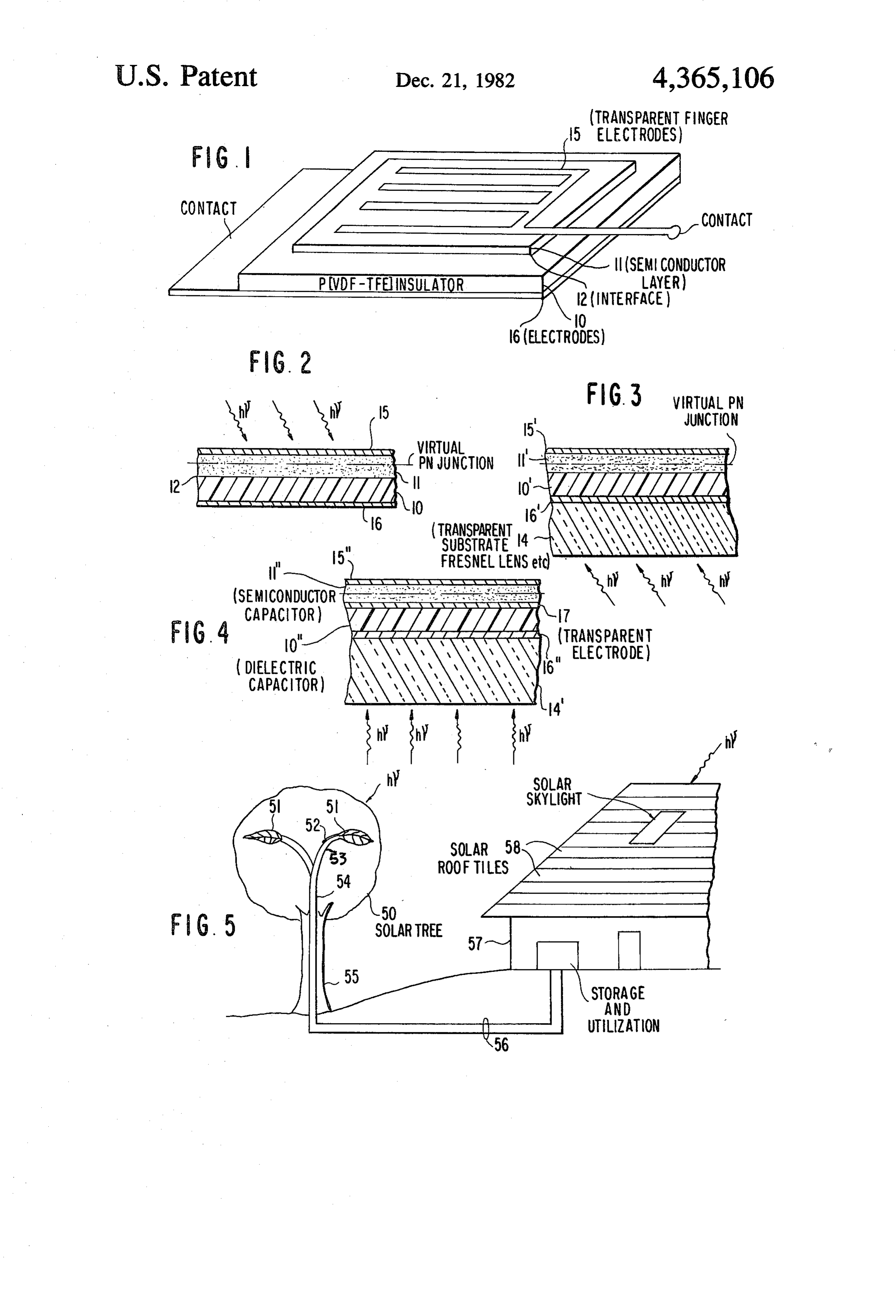
sidered in conjunction with the accompanying draw ings wherein:
CONVERTING SOLAR ENERGY TO ELECTRICAL FIG. 1 is an isometric view of a solar energy device ENERGY incorporating the invention.
REFERENCE TO RELATED APPLICATION FIG. 2 is a cross-sectional view of a portion of the devices illustrated in FIG. 1.
This application is a continuation-in-part of my appli FIG. 3 illustrates the modification of the device cation Ser. No. 069,477 filed Aug. 24, 1979 entitled shown in FIG. 2, “RADIENT ENERGY SYSTEMS, MEMORIES FIG. 4 is a further modification of the invention and, AND THERMAL IMAGING METHODS AND 10 FIG. 5 illustrates my solar tree and building.
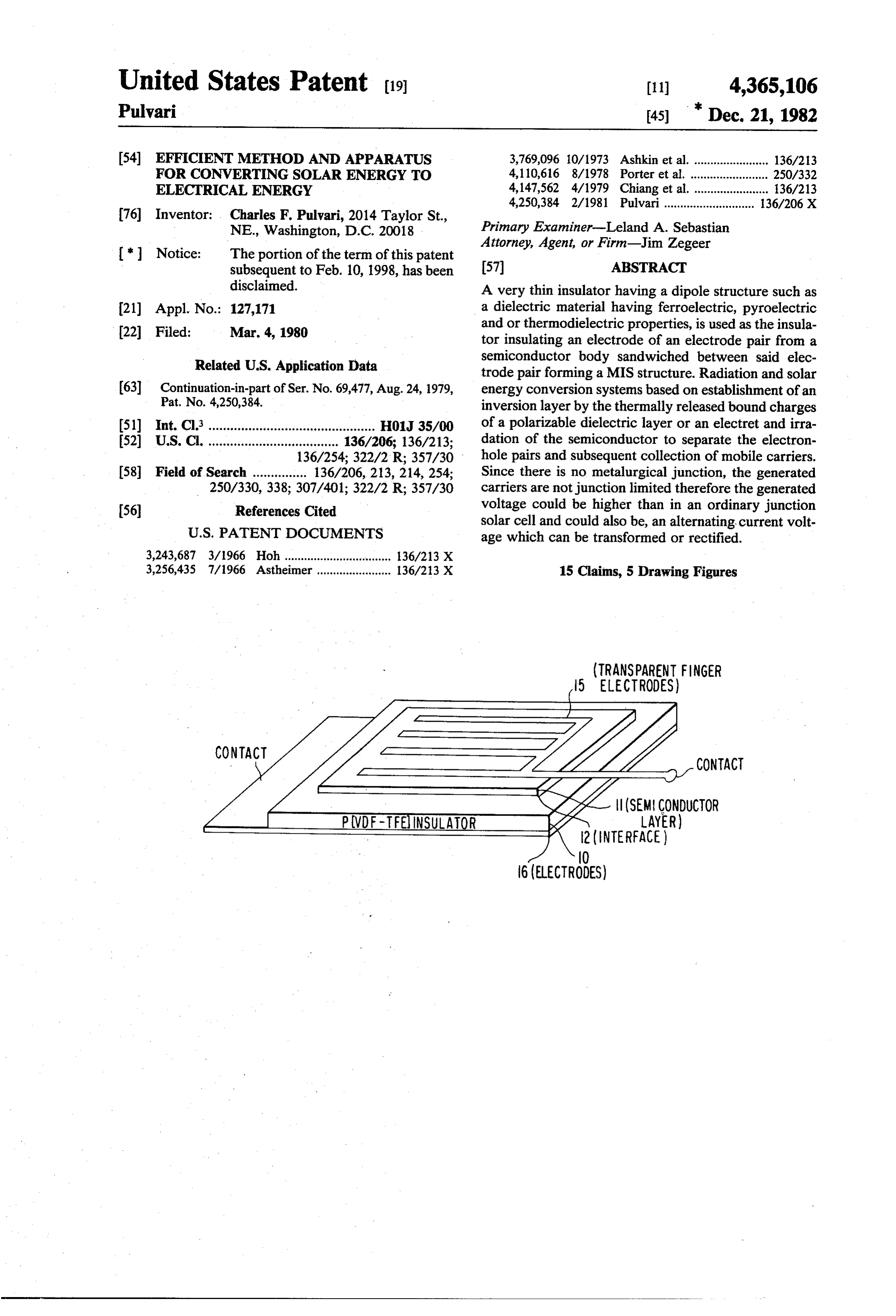
APPARATUS' now U.S. Pat. No. 4,250,384 issued With reference now to FIG. 1 of the drawings radia Feb. 10, 1981. tion or solar energy converter sensing device is shown BACKGROUND OF THE INVENTION wherein between two electrodes 15 and 16 a polarised thin insulating layer 10 constituted by a ferroelectric
Various forms of solid state solar energy conversion material and a thin semiconductor layer 11, the thin systems are known and used in the art with varying semiconductor layer being deposited, by vapor deposi degrees of economy, efficiency and ease of manufac tion on the ferroelectric layer to a few microns thick, tures, there being tradeoffs between each of these desir able goals. One form of energy conversion uses the for example. In the preferred embodiment, ferroelectric thermodielectric effect to convert solar radiation to 20 ment, 10 layer is a copolymer P(VDF-TFE). In this embodi electrical energy, as is disclosed in Hoh U.S. Pat. Nos. transparent90% the transparent finger electrode formed as 3,073,974 and 3,243,687, incorporated herein by refer substrate (see FIG.electrodes finger
is first formed on a glass followed by insulator 10, semi ence. The materials disclosed in the Hoh patents are in conductor layer 11 and metal electrode 15. the class of ferroelectric energy converters which are FIG. 2 shows a cross-section of the radiation i.e. solar very temperature dependent in the neighborhood of the 25 (sensing) energy converting device described in FIG.1. ferroelectric Curie point. The metal-insulator-semicon ductor (MIS) art is now well developed and infrared When irradiated, part of the absorbed radiation energy imaging systems using inversion mode operated MIS converts into thermal energy elevating the temperature devices with charge coupled devices (CCD), wherein of the whole capacitor structure, comprising the semi an inversion region or layer is created at the insulator- 30 conductor layer 11 and polarised insulator (for example semiconductor interface into which photogenerated a ferroelectric polymer) 10. When a polar dielectric in minority are collected are known, see the article by which a polarization exists is heated or cooled, a change Andrew J. Stecklet al entitled "Application of Charge in polarization with temperature occurs and the crystal Coupled Devices to Infrared Detection and Imaging', line or oriented polymer material develops an electric published in the IEE publication "Charge Coupled 35 charge on its surface, which in this case appears on the Devices: Technology and Applications' copyrighted in interface IF of the polarised insulator 10 and semicon 1977, and incorporated herein by reference. ductor 11. This charge layer generates a sufficient high The objects of the present invention include provid field and produces an inversion layer in the semicon ing improved radiation and solar energy conversion ductor body 11 indicated by 12 and creates a virtual systems and devices. In achieving these objects, the 40 P-N junction similar to the virtual P-N junction present invention, in one preferred mode, utilizes a very occuring in a MIS structure. Since another part of the thin ferroelectric material as the insulator of a MIS radiation spectrum generates electron whole pairs in the device. In another aspect of the invention, a very thin, semiconductor layer 11 these carriers will be separated low heat capacity ferroelectric material having thermo by the described virtual P-N junction, permitting the dielectric properties is utilized as the insulator in a MIS 45 photon to electron-whole pair converted electrical en device. In still another and preferred aspect of the in ergy to appear on the electrodes and to be utilized. vention solar energy is converted first into thermal and FIG. 3 illustrates a modification wherein one elec subsequently into electrical energy utilizing a thin ferro trode 16' is formed of transparent conductive electrode electric layer having pyroelectric properties, the thin material, such as doped tin oxide, on a substrate 14, ferroelectric layer constituting the insulator in a MIS 50 which could be glass or plastic and serves as a fresnel device, the voltage produced by the pyroelectric con lens to focus light, such as sunlight, on the transparent version in the ferroelectric layer operates to create an electrode 16'. Semiconductor layer 11' is transparent to inversion region or layer in the semiconductor body infrared and is formed as a thin layer or film on the and a virtual PN junction. In such state, the utilization dielectric by an epitaxial process. Ferroelectric layer 10 of the charge storage and transfer ability of an elec- 55 is the MIS insulating layer relative to the second elec troded polarized insulator (e.g. a ferroelectric body trode 16'.
member having dipole structure) and semiconductor This device is not energy gap limited and for solar interface affords the separation of electron whole pairs energy conversion purposes converts a large portion of and the taping of corresponding electrical energy. the spectrum of electromagnetic energy to electrical The thermally released electrical energy generated 60 energy. Since it is an inversion mode operated device by the polarisable dielectric appears on the surface of there is no physical junction and the epitaxial or poly the dielectric and is used only for causing the necessary crystalline layer can be extremely thin and the recombi bias for producing the inversion layer, which process nation effect is minimized. It is for this reason that a essentially does not consume much more energy than polycrystalline silicon material can also be efficiently needed to charge the virtual junction and most of which 65 and at much lower cost employed. charge is regained at the end of the cycle. It should be noted that the radiation not absorbed by The above and other objects advantages and features the ferroelectric capacitor will fall on the semiconduc of the invention will become more apparent when con tor capacitor and produce hole-electron pairs of large
Page 4
abundance because in absence of a physical junction, layer in a semiconductor body by applying a bias poten radiation having larger energies than the impurity, en tial to a pair of electrodes one of which is insulated from ergy levels will release, i-e excite (/e/-/h/) electron said semiconductor body, subjecting said inversion hole pairs, and the well caused by the inversion on the layer to one part of the incident solar energy radiation MIS interface will collect the mobile cariers. This spectrum to generate the electron /e/-hole /h/ pairs, unique interaction of the ferroelectric in the MIS capac and collecting the mobile carriers, the improvement itors results in a highly sensitive and effective radiation wherein the bias potential applied to said pair of elec conversion over nearly the whole radiation spectrum trodes is generated in situ by conversion of another and considerable higher voltage levels than the conven portion of incident solar radiation spectrum. tional photodiode devices. For this reason this biased 10 2. The invention defined in claim 1 wherein there is inversion layer structure converts a larger portion of established a plurality (n) of said inversion layers in a the radiation spectrum and is less energy gap limited as common semiconductor body being subjected to a por conventional junction devices are, because nearly 50% tion of the solar energy being converted to generate the of solar energy is in the infrared, which was lost with /e/-/h/ pairs in each portion of the semiconductor and photodiode type of conversion devices. The proposed 15 commonly collecting said charge carriers from all said improved radiation energy converter utilizes the infra charged layers.
red portion of the spectrum to heat with it the polarized 3. The invention defined in claim 2 wherein each of dielectric and thereby generate a much larger driving said inversion layers is formed by a MOS capacitor at potential across the virgual junction than the one avail the site of each semiconductor capacitor, generating a able on an ordinary P-N junction which is determined 20 bias potential unique to each site by a further solar to and limited by the difference of the fermi levels in the P electrical energy converter.
and N side of the junction. In this case the driving volt 4. The invention defined in claim 3 wherein each said age generated by the polarized dielectric would depend further solar to electrical energy converter is consti only on the thickness and the strength of polarization of tuted by a thermodielectric capacitor element. the dielectric and this could be orders of magnitude 25 5. A double capacitor comprising a pair of electrodes, higher than in P-N junction. The radiation conversion a thin dielectric layer and a thin semiconductor body efficiency of this biased inversion layer well solar en sandwiched between said pair of electrodes, said dielec ergy converter is therefore inherently higher than the tric layer being capable of converting infrared portions photodiode type and hence constitutes an improved of the radiation spectrum to a bias voltage for creating solar to electrical energy converter. 30 an inversion junction in said thin semiconductor body. FIG. 4 is again another modification of the present 6. A solar to electrical energy converting element invention illustrating a combination of the ferroelectric comprising a capacitor having a semiconductor body and semiconductor capacitors in such a manner that one member and at least one pair of electrodes and a second of their electrodes is united in a single common elec capacitor including a dielectric having a polarizable trode 17. 35 dipole structure coupled to said semiconductor capaci This novel solar to electrical energy converter ele tor in such a way that an inversion layer is in said semi ment can be utilized in a large number of ways for pro conductor body member, which when irradiated sepa ducing more powerful electrical energy generation; in rates the photon (hv) generated /e/-/h/ pairs and col the following only a few examples are presented to lects the mobile carriers in the inversion layer. illustrate the versatility of this novel device. The build 40 7. The solar energy converting sensing element de ing industry could have produced solar tiles, which fined in claim 6 wherein said second capacitor has ther could be applied on roofs, walls; another such applica modielectric properties.
tion could be semitransparent windows and sky lights 8. The solar energy converter defined in claim 6 producing electrical energy. Again other novel ar wherein said second capacitor is an electret. rangements and use for this novel device could be a 45 9. Solar to electrical power generator comprising a tree, the leaves of which are fabricated of a plastic based semiconductor capacitor having a semiconductor body small size solar converters from which the electrical member and at least one pair of electrodes, a solar to energy is collected through the busses in the branches electrical energy converter coupled to said semiconduc and trunk of the tree, the wind could serve for vibrating tor capacitor in such a way as to constitute a bias volt these leaves, thereby causing a useful cycling. This 50 age source and create an inversion layer in said semi avoids the unasthetic and architecturally depressing conductor body member such that when said semicon building structures currently used for collecting solar ductor body member is irradiated it generates the energy. As shown in FIG. 5 a solar tree 50 having /e/-/h/ pairs and collects the mobile carriers in said leaves 51 on branches 52 carrying leaf current collect inversion layer and means for extracting the electrical ing busses 53 to a trunk buss 54 in trunk. 55. There may 55 power generated from said pair of electrodes. be several solar trees supplying their electrical energy 10. Solar to electrical power generator as defined in to an underground line 56 leading to building 57. Build claim 9 wherein said semiconductor capacitor is charac ing 57 may be roofed with solar tiles 58 having the terized by a metal oxide semiconductor (MOS) capaci structure illustrated in FIG. 1 on a supporting ceramic tor with said at least one pair of electrodes being biased substrate. 60 by said solar to electrical energy converter so as to It will be appreciated that various modifications and establish said inversion layer.
changes will be obvious to those skilled in the art and 11. Solar to electrical power generator as defined in such modifications and changes are intended to be en claim 9 wherein one of said electrodes is transparent to compassed in the spirit of the invention as defined in the solar radiation.
claims. 65 12. Solar to electrical power generator as defined in I claim: claim 10 wherein said solar to electrical energy con 1. In a method of converting incident solar energy to verter is a ferroelectric pyroelectric capacitor intercon electrical energy comprising establishing an inversion nected with said MOS capacitor in such a way that
Page 5
when this MOS ferroelectric double capacitor is irradi 14. Solar to electrical power generator as defined in ated with infrared, the pyroelectric generated potential claim 13 wherein one of the electrodes on the ferroelec biases said MOS capacitor. tric capacitor is transparent to the radiation to be de 13. Solar to electrical power generator as defined in tected, and consists of two joint electrodes one of which claim 10 wherein said solar to electrical energy con is shared with the MOS capacitor while the other is verter includes a ferroelectric thermodielectric capaci. shared with the ferroelectric capacitor. tor interconnected with said MOS capacitor in such a 15. Solar to electrical power generator as defined in way that when the MOS-ferroelectric double capacitor claim 13 wherein one of the electrodes of both the MOS thus constituted is irradiated, the thermodielectrically capacitor and the ferroelectric capacitor is transparent generated potential biases the MOS capacitor to pro 10 to the radiation to be detected.
duce said inversion layer.
Provenance
- Collection
- Cited prior art
- Original PDF
- patentimages.storage.googleapis.com →
- Filed
- 1980-03-04
- Pages
- 5
- Method
- pdftotext (the PDF's own text layer) + pdftoppm 300dpi page scans
- Source
- Google Patents bibliographic record
- Granted
- 1982-12-21
- Inventors
- Charles F. Pulvari
- Transcribed from
- patentimages.storage.googleapis.com →