patent · US4088514
Method for epitaxial growth of thin semiconductor layer from solution
9 May 1978
Page 1 — bibliographic record
United States Patent (19) (11) 4,088,514 Hara et al. 45) May 9, 1978 (54) METHOD FOR EPITAXIAL GROWTH OF 3,950, 195 4/1976 Rode et al. ........................... 148/171 THIN SEMCONDUCTOR LAYER FROM Primary Examiner-G. Ozaki
SOLUTION
Attorney, Agent, or Firm-Robert E. Burns; Emmanuel 75 Inventors: Tohru Hara; Minoru Mihara; J. Lobato; Bruce L. Adams
Nobuyuki Toyoda, all of Kawasaki, 57 ABSTRACT
Japan
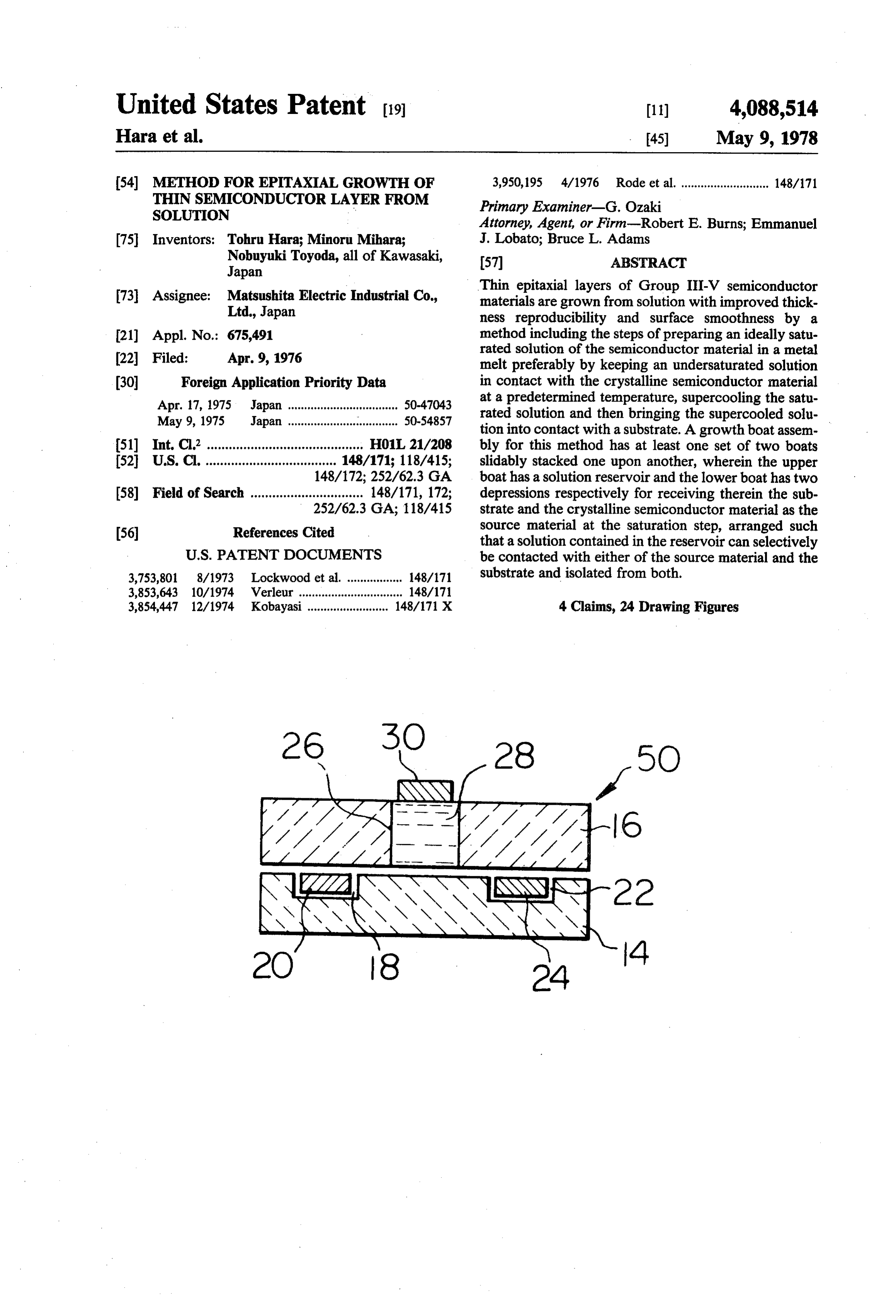
Thin epitaxial layers of Group III-V semiconductor 73 Assignee: Matsushita Electric Industrial Co., materials are grown from solution with improved thick Ltd., Japan ness reproducibility and surface smoothness by a (21) Appl. No.: 675,491 method including the steps of preparing an ideally satu rated solution of the semiconductor material in a metal (22) Filed: Apr. 9, 1976 melt preferably by keeping an undersaturated solution (30) Foreign Application Priority Data in contact with the crystalline semiconductor material Apr. 17, 1975 Japan .................................. 50-47043 at a predetermined temperature, supercooling the satu May 9, 1975 Japan .................................. 50-54857 rated solution and then bringing the supercooled solu tion into contact with a substrate. A growth boat assem (51) Int. C.’........................................... H01L 21/208 bly for this method has at least one set of two boats (52) U.S. Cl. .................................... 148/171; 118/415; slidably stacked one upon another, wherein the upper 148/172; 252/62.3 GA boat has a solution reservoir and the lower boat has two (58) Field of Search ............................... 148/171, 172; depressions respectively for receiving therein the sub 252/62.3 GA; 118/415 strate and the crystalline semiconductor material as the (56) References Cited source material at the saturation step, arranged such that a solution contained in the reservoir can selectively
3,753,801 8/1973 Lockwood et al. ................. 148/171 substrate and isolated from both. 3,853,643 10/1974 Verleur................................ 148/171 3,854,447 12/1974 Kobayasi......................... 148/171 X 4 Claims, 24 Drawing Figures
Page 2
Drawing sheet — no readable text.
Page 3
Drawing sheet — no readable text.
Page 4
Drawing sheet — no readable text.
Page 5
Drawing sheet — no readable text.
Page 6
Drawing sheet — no readable text.
Page 7
Drawing sheet — no readable text.
Page 8
pression for receiving therein a crystalline semiconduc
METHOD FOR EPITAXIAL GROWTH OF THIN tor material as a source material, which depressions are SEMICONDUCTOR LAYER FROM SOLUTION formed on the top face of the boat and spaced from one another.
This invention relates to a method for the liquid- 5 ture defining The second boat has a vertically bored aper phase epitaxial growth of thin layers of Group III-V on the top face a solution reservoir and is slidably placed semiconductor materials from solution and apparatus reservoir can beofselectively the first boat such that the solution positioned on the first de for performing the same. pression, on the second depression, and between and in Both liquid-phase and vapor-phase techniques have isolation from both of the first and second been used in the epitaxial growth of thin layers of 10 The boat assembly can be constituted of adepressions. multiplicity Group III-V semiconductor materials. Thin layers of substantially identical sets, e.g. 15 sets, of the first and grown by liquid-phase epitaxial techniques generally have advantages such as, for example, comparatively second boats. The first boat may have at least one addi tional first depression either with or without the addi few crystal defects, excellent layer-substrate interfacial tion of another second depression. characteristics and the ability of giving excellent junc- 15 A portion of the boat assembly which portion is in the tions. Accordingly, the epitaxial growth of thin layers form of a vertical column including the first depressions of Group III-V semiconductor materials such as, e.g., gallium arsenide, gallium phosphide and gallium alumi may be constructed as a detachable cassette so that the num arsenide from solution is widely used in the pro substrates depressions can be placed in and taken out of the first while the boats are in the assembled state.
duction of semiconductor devices which are required to 20
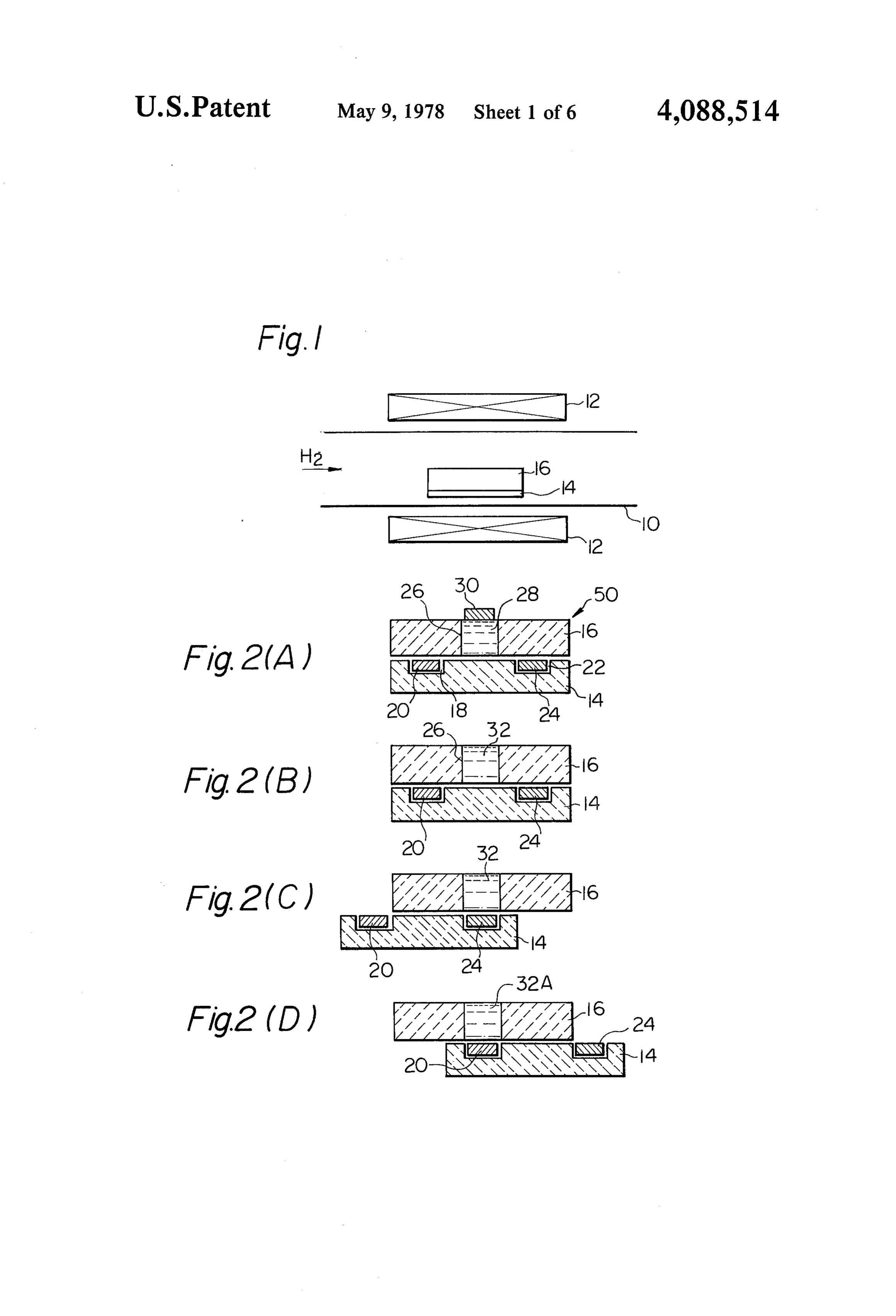
Other features and advantages of the invention will have excellent junction characteristics such as semicon become apparent from the following detailed descrip ductor double hetero LASERs, light-emitting diodes, tion of preferred embodiments with reference to the FET varactor diodes, Gunn diodes, IMPATT diodes accompanying drawings, wherein: and super lattice diodes. FIG. 1 is a schematic elevational view in section of a Conventional liquid-phase epitaxial growth methods, 25 liquid-phase epitaxial growth apparatus; however, are not completely satisfactory, particularly for industrial production of semiconductors, because of FIGS. 2(A)-2(D) are a series of schematic elevational various problems such as difficulty in precise control of views in section of a part of the apparatus of FIG. 1 both layer thickness and impurity concentrations, poor showing successive steps of a growth method according thickness reproducibility and unsatisfactory surface 30 to the invention;
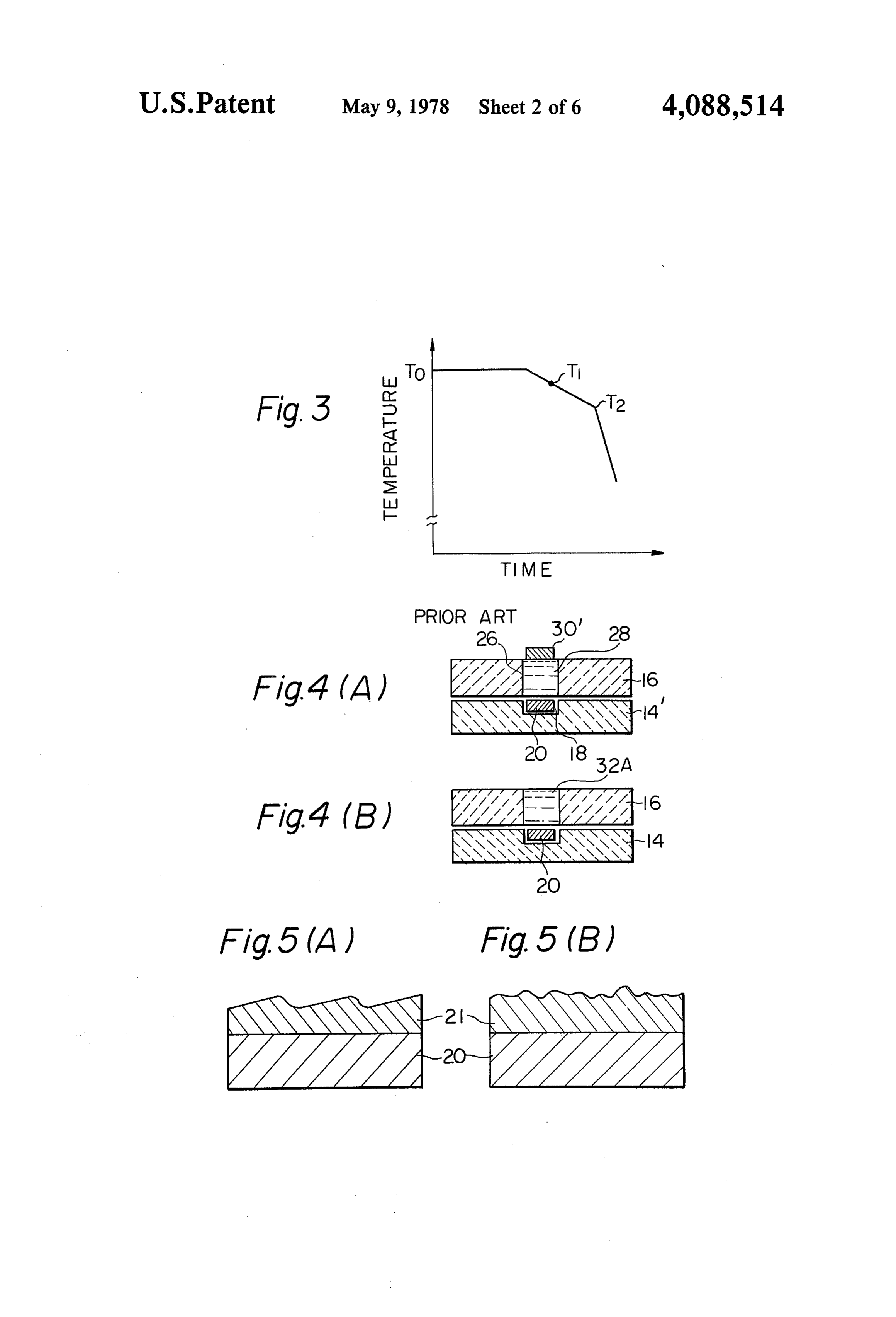
smoothness of the grown layers. These problems must FIG. 3 is a time-temperature profile of a cooling step be solved both to improve the quality and reproducibil in a growth method according to the invention; ity of the products and to reduce the cost of production; FIGS. 4(A) and 4(B) are a series of views fundamen however, these problems still remain unsolved. tally similar to FIGS. 20A)-2(D) but showing succes It is an object of the present invention to provide an 35 sive steps of a conventional growth method; improved method for the liquid-phase epitaxial growth FIGS. 5(A) and 5(B) are explanatory and sectional of thin layers of Group III-V semiconductor materials views of two representative semiconductor layers with from solution, which method brings about by an excel uneven surfaces grown by a method not in accordance lent reproducibility of the thickness of the grown layers, with the invention;
excellent surface smoothness of the grown layers, appli FIG. 6 is an elevational and sectional view of an cability to mass production and has little affect on mis essential part of a growth apparatus according to the orientations of the substrates. invention;
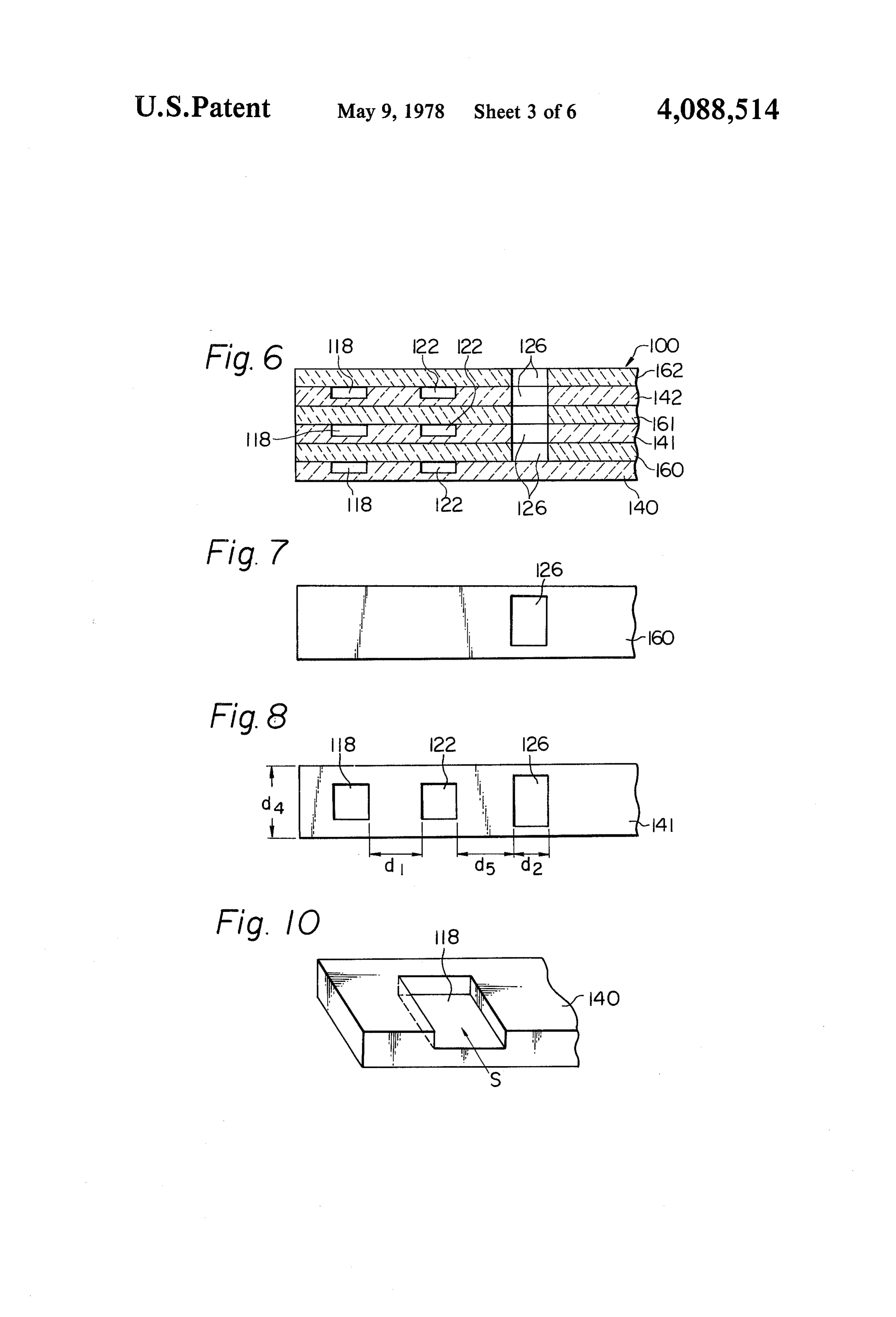
It is another object of the invention to provide an FIGS. 7 and 8 are plan views of two different ele improved apparatus for efficiently carrying out a liquid ments of the apparatus of FIG. 6, respectively; phase epitaxial growth according to the invention. 45 FIGS. 9(A)-9(D) are a series of views fundamentally According to the invention, a method for liquid similar to FIGS. 2(A)-2(D) but showing how the appa phase epitaxial growth of a thin layer of a Group III-V ratus of FIG. 6 is manipulated for carrying out a method semiconductor material on a substrate crystal from solu according to the invention;
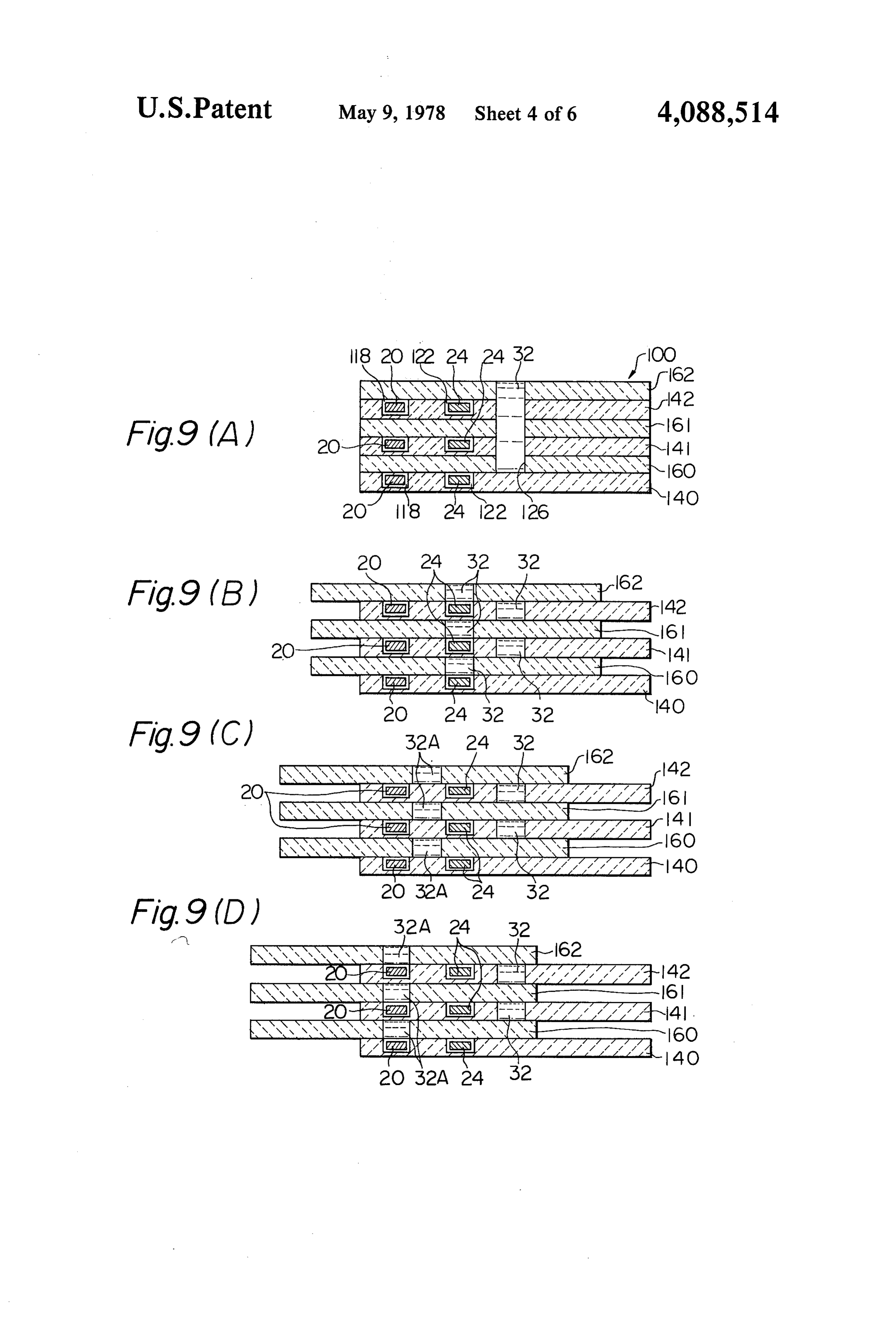
tion comprises the following steps: (a) preparing a FIG. 10 is an enlarged and perspective view of a part precipitate-free and ideally saturated solution of a 50 of the element of FIG. 8;
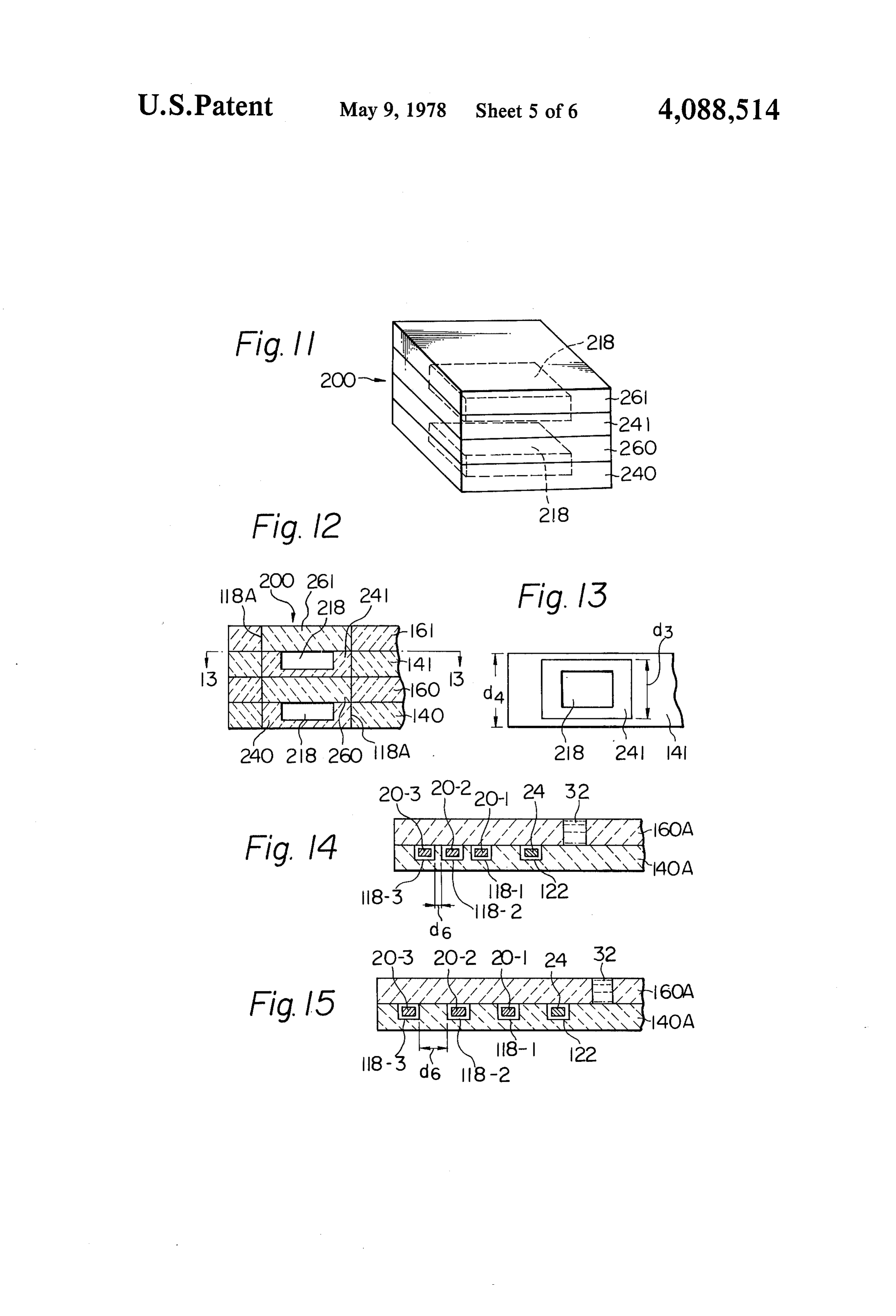
Group III-V semiconductor material in a metal melt at FIG. 11 is a perspective view of a substrate holder a predetermined temperature; (b) lowering the tempera devised for a growth apparatus which is a slight modifi ture of the ideally saturated solution to another prede cation of the apparatus of FIG. 6;
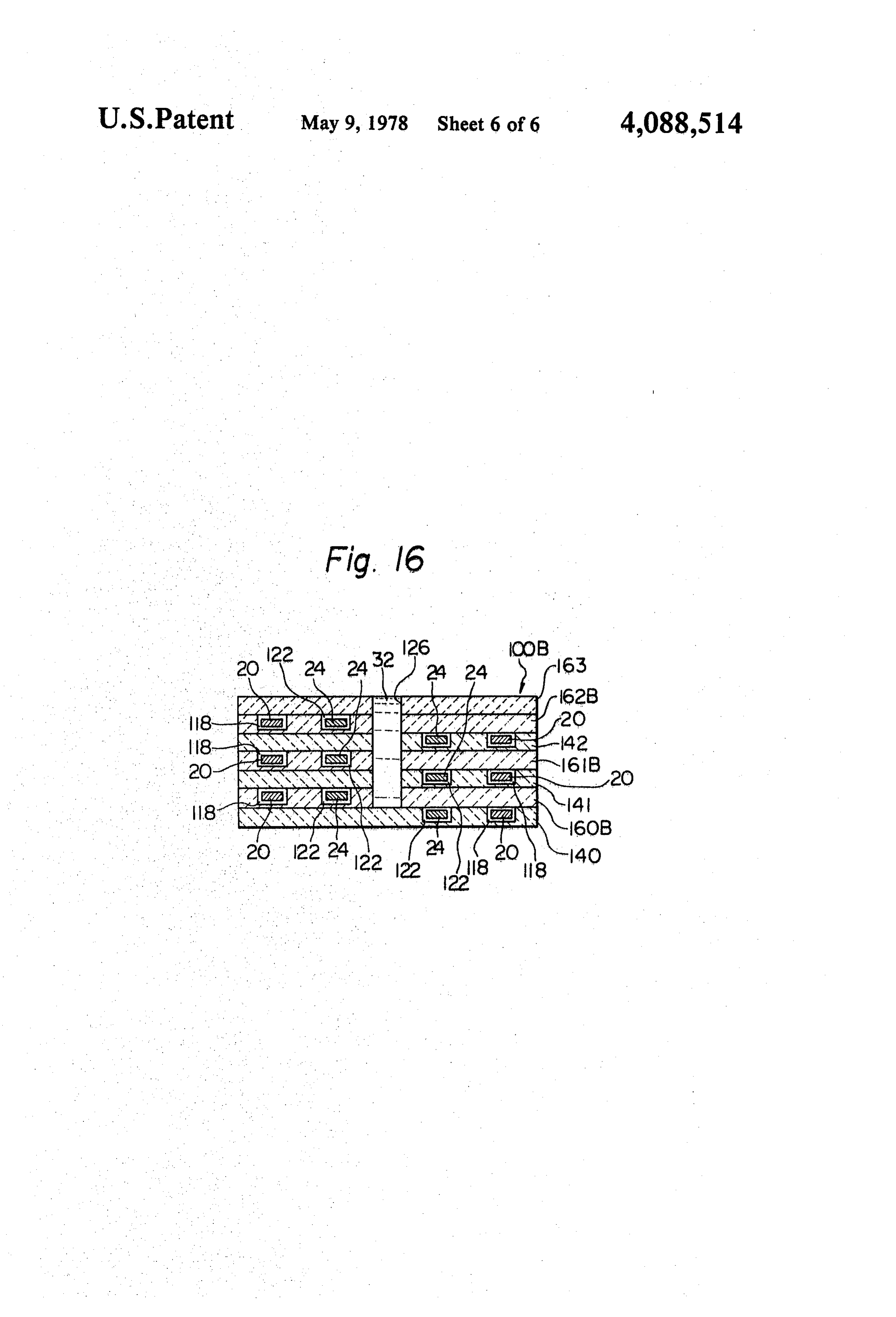
termined temperature to render it, a supercooled solu FIGS. 12 and 13 are respectively elevational and plan tion subsequently to separation of the ideally saturated 55 views in section of a part of a growth apparatus which solution from any source material; and (c) contacting is fundamentally the same as the apparatus of FIG. 6 but the supercooled solution with a substrate crystal. includes the element of FIG. 11; The ideally saturated solution is preferably prepared FIGS. 14 and 15 are elevational views in section by initially preparing an undersaturated solution at the respectively showing two different modifications of the first mentioned predetermined temperature and then growth apparatus of FIG. 6; and contacting the undersaturated solution with a separate FIG. 16 is fundamentally similar to FIG. 6 but shows source of the semiconductor material at the same tem a still different modification. perature to allow the solution to reach saturation The invention will hereinafter be described with re A growth boat assembly according to the invention spect to gallium arsenide as a typical example of Group comprises at least one set of first and second plate 65 III-V semiconductor materials. It will be understood shaped growth boats which are slidably stacked one from the essential features of the invention, however, upon another. The first boat has a first depression for that the invention is applicable to other III-V semicon receiving therein a substrate crystal and a second de ductor materials including ternary systems.
Page 9
The first procedure of a method according to the sembly 50 in this state is kept at 800° C for several hours invention for the growth of GaAs layers is the prepara to allow the GaAs crystals 30 to completely dissolve in tion of an ideally saturated Ga-As solution which con the Ga melt 28. As a result, the Ga melt 28 in the reser tains. As to the solubility limit of Ga-As system at a voir 26 turns to a Ga-As solution 32 as indicated in FIG. predetermined temperature but is utterly free from 2-(B). Since the amount of the dissolved GaAs 30 was GaAs precipitates. not enough to give a completely saturated solution, no As is known, it is difficult to practically prepare such solid-phase GaAs is present in the solution 32. an ideally saturated Ga-As solution. However, a re Then the lower boat 14 is moved to the left side in cently developed technique is useful for the method of FIG. 2 until the GaAs wafer 24 in the boat 14 comes the present invention. This technique employs a growth 10 into contact with the Ga-As solution 32 in the upper boat assembly consisting of a solution reservoir, a sub boat 16 as shown in FIG. 2-(C). In this state the GaAs strate holder and a thin slider which is sandwiched wafer 24 which has been kept at 800 C dissolves gradu between the reservoir and the substrate holder and ally into the solution 32 until the solution 32 becomes an which has an aperture. A large volume of source melt is ideally saturated solution as given by the Ga-As liquidus prepared in the reservoir by the use of Ga melt and a 15 curve at 800 C.
slightly excess amount of GaAs crystals. The source After this process, the lower boat 14 is returned to the melt is saturated by maintaining it at a predetermined initial position shown in FIG. 2-(B) where the ideally temperature, e.g. at 800 C, for a few tens of hours with saturated solution 32A is separated both from the sub precise temperature control. Then a small portion strate 20 and the GaAs source 24. In this state, the entire (which is called aliquiot) of the saturated solution is 20 system is cooled from 800 Cat a constant cooling rate. metered out from the bottom of the solution reservoir Referring to FIG. 3, the initial temperature, i.e., 800 C, into the aperture of the slider. The thus obtained thin is indicated at To When the temperature of the entire solution in the aperture of the slider is ideally saturated system reaches T, which is a few degrees below To as since no GaAs precipitate is present in the bottom re will hereinafter be described in detail, and the equili gion of a large volume of solution in the reservoir. 25 brated Ga-As solution 32A changes to a supercooled The present invention, however, provides as a part of solution, the boat 14 is moved to the right side until the the invention a more advantageous technique for the top surface of the substrate 20 comes into contact with preparation of an ideally saturated source melt as will the solution 32A over the whole area of the substrate 20 hereinafter be described. as shown in FIG. 2-(D). The cooling procedure is still Referring to FIG. 1, liquid-phase epitaxial growth of 30 continued, so that the temperature of the solution 32A thin layers in accordance with the invention is carried still becomes lower than T. Consequently, epitaxial out in a reaction tube 10 which is usually of quartz and growth takes place from the supercooled solution 32A stationarily held in an electric furnace 12. Two graphite on the surface of the substrate 20. It is an advantage of boats 14 and 16 are slidably assembled together in a this growth method that the precipitation of GaAs from piled arrangement and placed in the reaction tube 10. 35 the solution 32A occurs entirely on the substrate 20 in a Hydrogen as a carrier gas is introduced into the reac short growth time.
tion tube 10 during a growth run. The reaction tube 10 When the temperature of the entire system reaches and the furnace 12 are arranged such that the boat as T, which is usually a few degrees below T1, the boat 14 sembly 14 and 16 are entirely maintained in a uniform is moved again to the position shown in FIG. 2-(B) to temperature region. The apparatus and growth condi terminate the layer growth. After that the entire system tions are well known ones in these respects. is cooled to room temperature at a greatly increased The growth boats 14 and 16 for carrying out an epi cooling rate, and the substrate 20 is taken out of the taxial layer growth according to the invention are fun apparatus. In this cooling procedure, precipitation of damentally formed as shown in FIG. 2. In this case the GaAs takes place very uniformly in the solution 32A. It lower boat 14 serves as a wafer holder and is horizon 45 is important and necessary that this cooling procedure is tally movable. The lower boat 14 has a depression 18 in performed at a very high cooling rate in order to which a GaAs substrate wafer 20 is held and another quickly render the solution used in the above described depression 22 in which another GaAs wafer 24 as a growth run a uniformly dissolved Ga-As solution 32A source material is held. The upper boat 16 has an aper in a next run. In a next growth run, a separate substrate ture 26 which serves as a solution reservoir and initially 50 20 is newly placed in the depression 18, but there is no contains a quantity of Ga melt 28. Polyor single crystals need of renewing the solution 32 and the GaAs source of GaAs 30 are placed on the surface of the Ga melt 28 wafer 24 since the ideal solution 32A can again be pre as shown in FIG. 2-(A) in a quantity a little smaller than pared by repeating the same procedures with the same the quantity given by the Ga-As liquidus curve at a solution.
predetermined temperature. The shortage of the GaAs 55 The above described method is characterized in that crystals 30 to make a saturated solution at this stage is a the supercooled solution 32A is prepared by a three feature of the method according to the invention. The stage process: firstly, preparing an undersaturated solu amount of the GaAs crystals 30 to be added to the Ga tion, then bringing this solution into ideal saturation by melt 28 need not be measured precisely so long as it is the use of the GaAs wafer 24 placed in the depression guaranteed that the resulting solution remains undersat 22, and finally reducing the temperature with the ide urated at the predetermined temperature. It is prefera ally saturated solution being separated from the GaAs ble that the quantity of the GaAs crystals 30 is smaller source 24 and the substrate 20. This process may seem than the value given by the Ga-As liquidus curve at troublesome, but in reality brings about remarkable 800° C by about 5 to about 10%. savings of labor and raw materials in addition to a great Initially, the lower boat 14 is positioned as shown in 65 contribution of the supercooled solution to the quality FIG. 2-(A) so as not to allow any contact of the Ga melt of the grown layers.
28 with either the GaAs substrate 20 or the crystal In conventional liquid-phase epitaxial techniques to GaAs 24 contained in the depression 22. The boat as grow GaAs thin layers, the saturated GaAs solution
Page 10
32A is prepared by the following process. Referring to from the wafer 24. Besides, no unwanted precipitation FIG.4, the upper boat 16 for conventional layer growth on the surfaces or in the solution 32A occurs before and methods has the solution reservoir 26 which initially during the layer growth on the substrate 20. As a result, contains the Gamelt 28 in a manner similar to the upper the above described disadvantages of conventional liq boat 16 in FIG. 2. The lower boat 14' holds the GaAs uid-phase epitaxial growth methods are completely substrate 20 in the depression 18 but has no depression eliminated from a growth method according to the (22) for holding the GaAs source (24). In this case, invention. Thin (below 1.0 micron for example) GaAs GaAs crystals 30' are placed on the top of the Ga melt epitaxial layers can easily be grown by the method 28 as shown in FIG. 4-(A) in a precisely weighed quan according to the invention with excellent surface mor tity so that an exactly saturated Ga-As solution may be 10 phology and thickness control. This method is advanta obtained when the GaAs 30' is completely dissolved in geous also from the economical view-point since the the Ga melt 28 at an intended temperature, e.g., 800' C. Ga-As solution 32 can be used repeatedly, more than The dissolution of the source GaAs 30' is accomplished by keeping the boat assembly in the reaction tube 10 at ten times. As a still another advantage of this method, it is possible to moderate the requirement for precision in this temperature for 5-6 hours. When the dissolution of 15 the temperature control during the growth including GaAs is completed and the Ga melt 28 turned into the the solution preparation steps. In conventional methods, saturated Ga-As solution 32A, the epitaxial growth on it is necessary to control the temperature in the furnace the substrate 20 is initiated by the lowering of the tem 12 within 0.3C. Accordingly, the furnace 12 is nec perature of the entire system as described hereinbefore essarily of an extremely high grade. In the method of with reference to FIGS. 2 and 3. 20 the invention, the temperature control of -1.0° C suf This seemingly simple process has numerous disad fices to the success of the method. Accordingly, a com vantages in practical applications. mercially available and relatively inexpensive furnace (a) The quantity of the source GaAs 30' is determined can be used in the industrial production. on the basis of the relationship between the temperature The amount of the supercooling of the ideally satu and the solubility of GaAs in Ga, but this relationship is 25 rated Ga-As solution 32A, which is represented by the not yet exactly determined. Numerous reports have temperature difference AT = T - T, is an important been presented with disagreement between them: errors factor in a method of the invention. The surface mor of more than 5% have been recognized. phology, which may be evaluated quantitatively by the (b) It is also quite difficult to weigh a small quantity of surface roughness, of the grown layers is unsatisfactory GaAs with a satisfactorily high precision and good 30 either when AT is too large or when too small. In the reproducibility for each growth run. case of AT < 0.5 C, the so-called terrace morphology (c) Accordingly, the source GaAs 30' is usually used appears and becomes significant as AT approaches O'C, 10-20% in excess of a reported solubility. Alternatively, i.e. an equilibrated solution. The terrace morphology the dissolution of GaAs is carried out at an excessively disappears and very smooth layer surfaces are obtained high temperature, e.g., at 850 C, followed by a temper 35 when AT is between 0.5 C and 5 C. In most cases, ature reduction to the growth temperature, 800 C, to good surface morphology can be attained even if AT is prevent meltback of the substrate 20 into the Ga-As as large as about 10° C. The surfaces become uneven solution 32A upon contact of the substrate 20 with an when AT is larger than 10 C. However, it is preferable undersaturated Ga-As solution. Such meltback causes to carry out the supercooling according to the invention the surface of the substrate 20 to become uneven before under the restriction that 0.5 C S T S 5' C to attain the layer growth, and hence the grown layer will have the best surface morphology and thickness control. an uneven surface and/or unsatisfactory interface char acteristics. EXAMPLE 1 (d) The presence of excess GaAs in the saturated The growth apparatus of FIGS. 1 and 2 was used. solution 32A has great and unfavorable influences on 45 The undersaturated Ga-As solution 32 was prepared the surface morphology of the grown layer and on the from 20g of pure Ga as the melt 28 in the reservoir 26 reproducibility of the layer thickness and/or surface and 0.80g of polycrystalline GaAs 30 which was placed morphology. Homogeneous nucleation chances to on the Ga melt 28. This example was for the epitaxial occur prior to layer growth and adversely affects the growth of an n-type thin GaAs layer, so that 0.40g of Sn surface morphology of the grown layer. In addition, a 50 was doped to the Ga melt 28. Of course, other kinds of large portion of GaAs is precipitated on the surface of usually employed impurity elements may be added to the solution 32A. Accordingly, the liquid-phase epitax the Ga melt 28 and/or the crystalline GaAs 30. For ial growth of GaAs on the substrate 20 is significantly example, Si, Te or Se other than Sn as an n-type impu affected by these unintentional precipitations of GaAs. rity and Zn, Geor Si as a p-type impurity may be used. Since such unintentional precipitation of GaAs does not 55 The crystalline GaAs 30 may be doped with Cr, Mn or occur uniformly in every growth run, neither the layer NH.
thickness nor the surface morphology of the grown A 20 x 20mm wide and 1mm thick polycrystal GaAs layer is reproducible in successive runs. Therefore, wafer was placed in the depression 22 of the lower boat certain measures must be taken to eliminate any unin 14 as the supplementary GaAs source 24. The substrate tentional precipitation in Ga-As solution 32A. 20 was a 20 X 20mm wide and 0.3mm thick wafer of (e) An unnecessarily large quantity of Ga which is Cr-doped semiinsulating GaAs. The substrate crystal 20 very expensive is needed to prepare the Ga-As solution was preliminarily subjected to a usual surface polishing 32A, and renewal of the solution 32A (Ga melt 28) is procedure and then to a chemical etching in a bromine necessary for every growth run. methanol system. The source wafer 24 also was used In the method according to the invention, the weigh 65 after chemical etching.
ing of the source GaAs 30 need not be performed with To dissolve the crystalline GaAs 30 in the Ga melt 28, high precision because the solution 32 can be brought to the boat assembly 50 was maintained in the position an ideal saturation by the subsequent supply of GaAs shown in FIG. 2-(A) and heated gradually in H, gas
Page 11
stream of 300 ml/min. When the temperature reached pends on the thickness of the grown layers, thickness of 5° C below the intended growth temperature of 800' C, the solution 32 and/or the kind and concentration of the the heating rate was lowered to 10 C/min so that the added impurity. It is possible to further increase the temperature of the melt 28 would not exceed 800° C. number of repetitions by replenishing the impurity and The entire system was kept at 800° C in the H gas /or the crystalline GaAs 24 in the course of the repeated stream for more than 6 hr. By this process, the source growth runs.
GaAs 30 was completely dissolved in the Ga melt 28.
The As concentration in the thus prepared solution 32 EXAMPLE 2 was about 10% below the solubility limit of Ga-As This example was generally similar to Example 1, but system at 800° C. 10 the unsaturated solution 32 was prepared by dissolving Then the lower boat 14 was moved and positioned as 88mg of GaAs crystals (30) in 2.2g of Ga (28). Since the shown in FIG. 2-(C), so that the solution 32 was al same upper boat 16 was used in this example as in Exam lowed to be in contact with the source GaAs wafer 24 ple 1, the thickness of the solution 32 was far smaller which also had been kept at 800 C. The source GaAs than in the case of Example 1. A graphite block (not 24 dissolved gradually in the undersaturated solution 15 shown) was placed, therefore, on the surface of the 32, and the ideal solution 32A which was in exact agree solution 32 as a weight mass so that the unsaturated ment with the solubility limit of Ga-As system at 800 C solution 32 and the saturated solution 32A would thor was obtained in less than 3 hr. Then the lower boat 14 oughly wet the surfaces of the source GaAs 24 and the was again brought into the position of FIG. 2-(B) to substrate 20, respectively. As a result, epitaxial layers separate the solution 32A from the source GaAs 24, and 20 grown in this example were substantially the same as the boat assembly 50 was cooled from 800 C at a con the layers grown in Example 1 in their surface smooth stant rate of 0.5 C/min. It is an important feature of this ness. The growth run was repeated many times with invention that the ideal solution 32A (in which no solid excellent thickness reproducibility: layers of phase GaAs exists at 800° C) be kept out of contact with 0.6-0.4m were grown. The scattering of the layer both the substrate 20 and the source GaAs 24 during 25 thickness in this example was quite narrower than, i.e. this cooling process. When the temperature reached about 1/10 of, the scatterings in conventional methods. 797° C (T. in FIG. 3), the lower boat 14 was moved to The use of a thin solution 32 has the advantage of an take the position of FIG. 2-(D) to bring the solution improved productivity (a shortened growth time in 32A into contact with the substrate 20 over the whole each run). In Example 2 it was possible to shorten the area. Since the cooling was not interrupted, the epitaxial 30 time needed to accomplish each growth run in Example growth of GaAs on the substrate 20 commenced upon 1 by about 20 to about 35%.
its contact with the supercooled solution 32A. The The growth method according to the invention has lower boat 14 was kept in this position for about 30 sec also the advantage that the surface of the grown layer is until the temperature reached 796.75° C. Then the boat extremely smooth practically regardless of crystal ori 14 was returned to the position of FIG. 2-(B) to termi 35 entation of the substrate 20.
nate the growth. It is well known in the art of epitaxial layer growth Thereafter the cooling rate was increased to more that the surface morphology of a grown layer is signifi than 30 C/min, and the entire system was cooled to cantly affected by the misorientation of a substrate from near room temperature with a continued care for uni a low index plane. For example, in the vapor-phase formly cooling the entire system. Then the boat assem epitaxial growth of silicon gallium arsenide and gallium bly was taken out of the reaction tube 10, and the sub phosphorus arsenide, thin layers with smooth surfaces strate 20 was taken out. The epitaxial layer grown on can be grown on small misoriented substrates. The in the substrate 20 in this example was 0.5um thick and fluence of the crystal orientation is more significant in was excellent in surface morphology. The surface liquid phase epitaxial growth. In the conventional liq roughness of this expitaxial layer was far smaller than 45 uid-phase epitaxial growth of gallium arsenide or gal i200 A. The grown layer was of n-type GaAs with lium phosphide, layers having good surfaces can be carrier concentration of 1 x 107 cm. grown only on the substrates whose misorientation is Another but identical substrate 20 was placed in the not greater than 0.1. If misorientation is greater than depression 18 of the same boat 14, and the boat assembly 0.1 from a low index plane, the surface of the grown 50 was again placed in the reaction tube 10. The solu 50 layer is uneven and a terrace morphology appears. The tion 32 and the source GaAs 24 which had been used in unevenness becomes more significant with increase in the above described run were used again. The boats 14 the misorientation of the substrate. and 16 were positioned as shown in FIG. 2-(B) and kept In slicing substrate wafers from a GaAs ingot, wafers at 800° C for about 30 min. Although the solution 32 of better than about 0.2 in misorientation cannot be had been cooled at the end of the preceding run, the 55 obtained on production scale because various angular undersaturated solution 32 was regained in quite a short errors are introduced during the following procedures. time because the precipitation of GaAs had taken place (a) Attachment of the ingot to a slicing machine. (b) very uniformly in this solution. Thereafter the solution Successive slicing works to obtain many wafers from a 32 was contacted with the source GaAs 24 in the same single ingot. (c) Polishing and chemical etching of the manner as in the preceding run to prepare the ideally sliced wafer. When errors for these reasons are summed saturated solution 32A. The temperature program and up, the misorientation of the substrate 20 easily becomes growth procedure were in exact accordance with those greater than +1.5 in industrial production. It is very of the preceding run. The layer thickness, carrier con difficult and expensive, therefore, to produce substrates centration and surface morphology of the thus grown of such a small misorientation as 0.2. layer were the same as in the previously grown layer. 65 When a GaAs wafer which was about 0.2 off from This example can be repeated more than ten times the <100) orientation (this inclination angle will here without renewal of the solution 32 and the source GaAs inafter be called "off-angle') was used as the substrate 24. The maximum possible number of repetitions de 20 for the growth of a 0.5um thick GaAs epitaxial layer
Page 12
by a conventional solution growth method (using a required of the lower boat 14 by the novel method as slightly oversaturated Ga-As solution in equilibrated will have already been understood from the foregoing state and the same growth temperature profile as in description with reference to FIG. 2. Example 1), the grown layer had a considerably rough This invention provides, however, a further im surface (a surface roughness of about hil000 A). The proved apparatus or growth boat assembly for industri surface roughness became more significant as the off ally carrying out the growth method according to the angle of the substrate 20 increased. If a 0.5um thick invention. As described hereinbefore, the reaction tube GaAs epitaxial layer is grown on a GaAs substrate with 10 and the furnace 12 need not to be designed differ 0.2 off-angle from the <100d plane by a conventional ently from those which are used in conventional solu solution growth method, the layer has an uneven sur 10 tion growth methods except that the furnace 12 may be face and is not suitable to the production of semicon of a less precise type. Accordingly, the description of ductor devices. the improved apparatus will hereinafter be presented By the liquid-phase epitaxial growth method accord only with regard to a growth boat assembly. ing to the invention, the layer surface is satisfactorily Referring to FIGS. 6-8, a growth boat assembly 100 smooth or mirror-like even when a substrate 20 with a 15 is primarily different from the boat assembly 50 of FIG. very large off-angle is used as will be illustrated by the 2 in that the former 100 is made up of six sheets of following example. graphite plates or boats which are stacked one upon EXAMPLE 3 another. The number of these boats is not necessarily limited to six but may optionally be chosen. If the fur
The ideally saturated Ga-As solution 32A was pre 20 nace 12 is of a diffusion type as commonly used in the pared according to Example 2. The substrate crystal 20 production of silicon transistors having a constant tem of Cr-doped GaAs was of 1.5' off-angle from the perature (-1 C) heating zone of 100mm in diameter <100> plane. The saturated solution 32A was cooled and 1300mm in length and the reaction tube 10 is 80mm from 800' C(T) at the same rate as in Example 2 in in diameter and 1800mm in length, the boat assembly order to prepare the supercooled solution 32A. The 25 100 may consist of up to 30 boats. These six boats are supercooled solution 32A was brought into contact identified by numerals 140, 160,141, 161,142 and 162 in with the substrate 20 when the temperature reached the stacked order starting from the lowermost boat 140. 798 COT) to grow a 0.5pm thick layer. The surface The boats 160, 161 and 162 have an identical plan view morphology of the thus grown layer was excellent: the as shown in FIG. 7. Each of these three boats 160, 161 surface roughness was far smaller than t200 A. 30 and 162 has a vertically bored aperture 126 which This example was repeated by the use of GaAs sub serves as a solution reservoir like the reservoir 26 of the strates 20 with different off-angles of 2.5, 5, 7 and 15 upper boat 16 in FIG. 2. The boats 141 and 142 are degrees, respectively. The surface morphology of the identical with one another and have a plan view as layers grown on these substrates 20 also was excellent. shown in FIG.8. Each of these two boats 141 and 142 The temperature difference, AT= To-Ti, is an im 35 also has the solution reservoir 126 with the same cross portant factor on the surface morphology of the layer section and at the same location as the reservoirs 126 of grown by the method according to the invention and the boats 160, 161 and 162. In addition, a depression 118 should be determined within a certain range, which is for holding therein the substrate 20 and another depres variable depending on other factors such as the temper sion 122 for holding therein the crystalline source mate ature at which the growth is initiated, the cooling rate rial 24 are formed in the top face of each of these two for the growth, the thickness of the layer, the thickness boats 141 and 142 such that the depression 122 is spaced of the solution 32A and the off-angle of the substrate 20. from and located between the reservoir 126 and the With respect to the growth of GaAs layers according to depression 118. As in a conventional boat assembly, the the foregoing examples, it was possible to grow the cross section of the reservoir 126 is equal to or slightly layers with glassy surfaces by determining the tempera 45 larger than the cross section of the depression 118. The ture difference AT within the range between 0.5 and 5 distance indicated at d between the two depressions 118 C. When the off-angle of the substrate 20 was 1.5 and and 122 is longer than the length d of the reservoir 126. the temperature difference a T was smaller than 0.5 C, The lowermost boat 140 is identical with the boats 141 the terrace morphology appeared on the surface of the and 142 having the depressions 118 and 122 except for grown layer as shown (in exaggeration) in FIG. 5-(A) 50 the omission of the reservoir 126. despite the ideal saturation and supercooling of the Thus, it will be understood that the six boats of this solution 32A. When AT was larger than 15 C, the assembly 100 can fundamentally be divided into two surface of the grown layer was irregularly uneven and groups, a first group which consists of the boats 160, 161 undulated as shown in FIG. 5-(B). and 162 having neither of the depressions 118 and 122 It will be understood from the nature of the invention 55 and a second group which consists of the boats 140,141 that the method of the invention is applicable to various and 142 having the depressions 118 and 120, and that Group III-V semiconductor materials (including ter each of the first group boats 160,161 or 162 is placed on nary systems) exemplified by Gap, InP, InAs, GaSb, each of the second group boats 140, 141 or 142. Each InSb and GaAlAs by choosing an appropriate time boat in the assembly 100 of FIG. 6 is in slidable relation temperature profile. For example, epitaxial layers of to the adjacent boats, and the boats of one group (boats GaP can be grown in accordance with Example 1 or 2 140,141 and 142 in this case) are placed stationary in the except for a rise of Toby about 100° C. reaction tube 10. The remaining boats 160, 161 and 162 As to the apparatus for carrying out the growth can be moved simultaneously both to the right and to method according to the invention, apparatus for con the left in FIG. 6 from the outside of the reaction tube ventional liquid-phase epitaxial growth methods can be 65 10 by a driving means such as a push rod (not shown). used only with a slight modification of the lower boat Also it will be understood that the boat assembly 100 14, because only the provision of the depression 22 for consists substantially of three sets of the boat assembly holding the crystalline source material 24 is essentially 50 of FIG. 2 only with additional provision of the reser
Page 13
voir 126 in the lower boat 14 for each set except one set 122 illustrated in FIG. 9. With 300mm long boats, it is which is placed at the bottom of the assembly 100. A possible to form three pairs of the depressions 118 and plurality of sets of boat assembly 50 of FIG. 2 are piled 122 in each of the boats 140, 141 and 142. Accordingly, up together to give the assembly 100 of FIG. 6 for the epitaxial layers can simultaneously be grown on up accomplishing the epitaxial layer growth simulta to 45 (3 x 30/2 sheets) pieces of the substrates 20 in the neously on a plurality of substrates 20 in a single growth reaction tube 10 of about 80mm in diameter. run and gaining a full advantage from the solution 32 The GaAs solution 32 in the reservoirs 126 of the prepared according to the invention. three boats 160, 161 and 162 can be used repeatedly The operation of this boat assembly 100 will be de simply by the steps of heating the boat assembly 100 scribed with reference to FIG. 9. Initially, the six boats O while in the position are arranged as shown in FIG. 6 or FIG. 9-(A) so that 30 minutes and then maintainingof FIG. 9-(C) at 800° C for about the solution reservoirs 126 of the five boats 160, 141, the assembly 100 in the 161, 142 and 162 may vetically be in exact alignment, position of FIG. 9-(B) until the solution 32 again and these reservoirs 126 are filled with the undersatu reaches ideal saturation by the replenishment of GaAs rated GaAs solution 32 (the As concentration in this 15 from the GaAs sources 24. The solution 32 as well as solution 32 is preferably 5-10% below the solubility in the GaAs source 24 can usually be used more than ten the Ga melt 28 at the employed temperature, e.g., 800 times in repetition. It is required of the boat assembly C, as described hereinbefore). The GaAs substrate 20 100, therefore, that the substrates 20 can be renewed and the GaAs wafer 24 as the supplementary source without disassembling the boat assembly 100. Accord material for the solution 32 are placed respectively in 20 ingly, each depression 118 in FIG. 6 is formed to reach the depressions 118 and 122 of each of the stationary one lateral side of each of the boats 140, 141 and 142 as boats 140, 141 and 142 as illustrated in FIG. 9-(A). The shown in FIG. 10. The substrate 20 is inserted into the depression 118 is so devised as to be able to admit and thus formed depression (or an open-ended slot) 118 detach the substrate 20 even when the six boats are transversely to the boat 140, 141 or 142 as indicated by assembled together and kept in the state of FIG. 9-(A) 25 the arrow S in FIG. 10. When a growth run is com as will hereinafter be explained.
Then the boats 160, 161 and 162 are simultaneously pleted in FIG.
and the boat assembly 100 is positioned as shown 9-(C), the substrates 20 can be taken out of the moved to the left to bring the unsaturated solution 32 in depressions 118 either by tilting the boat assembly 100 the reservoirs 126 of these boats 160, 161 and 162 into contact with the source GaAs 24 in the boats 140, 141 30 or by the use of a pair of thin tweezers. and 142 as shown in FIG. 9-(B). When the undersatu andFIGS. 11-13 show another method for easy loading rated solution 32 turned into the ideally saturated solu 200 removal
of the substrates 20. In this case, a cassette prepared as a detachable element of the boat tion 32A, the three boats 160, 161 and 162 are simulta neously moved further to the left so that the reservoirs assembly 100. This cassette 200 consists of the same 126thereof may be isolated from both the GaAs sources 35 number of graphite plates as the boats which constitute 24 and the substrates 20 as shown in FIG. 9-(C). In this the boat assembly 100. (FIGS. 12-14 show a case when state, the entire assembly 100 is subjected to a tempera the total number of the boats is four). The graphite ture reduction from 800 C at a constant rate of, e.g., plates 240, 260, 241 and 261 of the cassette 200 are 0.5 C/min. stacked one upon another in the same manner as the When the temperature reaches a predetermined tem boats 140, 160, 141 and 161 of the boat assembly 100 and perature indicated at T in FIG. 3, the three boats 160, have respectively the same thicknesses as the corre 161 and 162 are simultaneously moved to the left until sponding boats. The cassette 200 is smaller in width the supercooled solution 32A in the reservoirs 126 indicated at d, in FIG. 13 than the width d of the boat thereof come into contact with the substrates 20 as assembly 100. Each of the graphite plates 240 and 241 shown in FIG. 9-(D) with continued cooling. Since the 45 which correspond respectively to the boats 140 and 141 temperature is decreasing, GaAs begins to separate has a depression 218 for receiving the substrate 20. The from the solution 32A and epitaxially grows on the plates 260 and 261 are slidable with respect to the plates substrates 20. When the layers are grown to the in 240 and 241. The depressions 118 of the boats 140 and tended thickness at the temperature of Tin FIG. 3, the 141 are replaced by vertically bored apertures 118A three boats 160, 161 and 162 are simultaneously moved 50 with the same cross section as the cassette 200, and the to the right until the assembly 100 takes the position shown in FIG.9-(C). Thereafter the entire assembly 100. boats such a 160 and 161 also have the same apertures 118A at location that the apertures 118A in all the boats is cooled at an increased rate to near room temperature, 140, 160, 141 and 161 are vertically in alignment as and the substrates 20 are taken out of the depressions shown in FIG. 12 when the boat assembly 100 is 118. The thus grown layers on the three substrates 20 55 are excellent in the surface morphology and practically brought to the position shown in FIG. 9-(C). The sub identical with each other. strates 20 are placed in the depressions 218 of the graph As will have been understood, the layers can simulta bledite plates 240 and 241, and then the cassette 200 is assem neously be grown on a plurality of substrates 20 (numer as shown in FIG. 11. The assembled cassette 200 is ically, of the total number of the boats in the boat inserted downwards into the aligned apertures 118A of assembly 100) in a single run. the boat assembly 100 which is kept in the position of Since the depressions 118 and 122 are very short in FIG. 9-(C). When a growth run in completed and the length relative to the boats, it is possible to further in boat assembly 100, takes the position shown in FIG. crease the number of layers (i.e., the number of the 9-(C), the cassette 200 is taken out of the apertures 118A substrates 20) grown in a single run by forming at least 65 followed by the insertion of another cassette 200 con one additional pair of the depressions 118 and 122 in taining fresh substrates 20 for the next run. each of the boats 140, 141 and 142 in the same arrange The following Example 4 illustrates the use of the ment as and on the left side of the depressions 118 and boat assembly 100 (thirty boats) of FIG. 6.
Page 14
EXAMPLE 4 roughness of the grown layers in this example was below 200 A.
The reaction tube 10 was 85mm in diameter and EXAMPLE 5 about 1800mm in length including constricted end sec tions, The furnace 12 had about a 450mm long heating 5 This example was fundamentally similar to Example zone in which the temperature could be controlled 4, but each of the fifteen boats represented by the boats within it:1" C. Thirty boats constituted the boat assem 140, 141 and 142 had two additional pairs of the depres bly 100, but reference will be made to the six-boat as sions 118 and 122 which are respectively filled with the sembly 100 of FIGS. 6 and 9 for convenience. Each substrates 20 and the GaAs sources 24. When the graphite boat was 40mm wide (d. in FIG. 13), 300mm O growth on the substrate 20 placed in the extreme right long and 2mm thick. one of the three depressions 118 was completed, the . In a separate boat (not shown) which was placed in a solution 32 in each of the boats represented by 160, 161 separate reaction tube, a Ga-As solution 32 was pre and 162 was kept in contact with the GaAs source 24 in pared by dissolving 4,2g of GaAs polycrystals and 2.0g the middle one of the three depressions 122 and heated of Sn (as an n-type impurity) in 140g of Ga melt which 15 at 800 C for 30 min to replenish the GaAs component was maintained at 800' C in a Hstream for 20 hr. The consumed by the preceding layer growth. The GaAs As concentration in the resulting solution 32 was layers grown in this Example were of the same quality 5-10% below the solubility in Ga at 800° C. This solu as the layers obtained in Example 4. tion 32 was rapidly cooled (at a rate of 20 C/min) and When it is intended to form a plurality of depressions poured into the solution reservoirs 126 of the boat as 20 118 for holding the substrates 20 in each of the boats sembly 100 which was in the position shown in FIG. 140, 141 and 142, the depression 122 for holding the 9-(A). GaAs source 24 need not necessarily be formed in plu The substrates 20 were prepared by subjecting 20 X ral so as to individually pair with the depression 118, 20mm wide and 30pm thick Cr-doped (20x10'cm) but, alternatively, a single depression 122 may be n-type GaAs wafers to usual polishing and chemical 25 formed for a plurality of depressions 118 in the follow etching treatments, The GaAs sources 24 were pre ing manner. Referring to FIG. 14, the boat 140A has pared by treating 20X20mm wide and 300pm thick three identical depressions 118-1, 118-2 and 118-3, and wafers of Sn-doped (5,0x10cm) n-type GaAs simi one depression 122. In this case, the distanced between larly to the substrates 20. the depression 118-2 and either the depression 118-1 or The solution reservoirs 126 of the boats were 20mm 30 118-2 is made shorter than the length of the depression in length (d. in FIG. 8). The distance (d. in FIG. 8) 118. In operation, the solution 32A in the reservoir 126 between the reservoir 126 and the depression 122 was is brought into contact with the three substrates 20 in 5mm, and the distance d between the depressions 118 the three depressions 118-1, 118-2 and 118-3 one by one and 122 in the boats 140, 141 and 142 was 30mm. Both in numerical order. Since the layer growth on the re depressions 118 and 120 were 20mm long and 20mm 35 spective substrates 20-1, 20-2 and 20-3 takes place at wide. different temperatures from the solution 32A whose The substrates 20 and the GaAs sources 24 were state is varying, the growth time should be progres placed in the depressions 118 and 122 of the fifteen boats sively increased for the substrates 20-2 and 20-3 if it is represented by boats 140, 141 and 142. The boat assem desired to grow the three layers to the same thickness. bly 100 in the state of FIG.9-(A) was maintained at 800 In FIG. 15, the three depressions 118-1, 118-2 and C in a stream of H for 30 min. Then the fifteen boats 118-3 are spaced from each other such that the distance represented by boats 160, 161 and 162 were moved to dis equal to the length of the depressions 118. In opera the left in FIG, 9 at a constant speed of 20mm/sec to tion, the solution 32A was kept in contact with the boat bring the boat assembly into the position shown in FIG. 140A at a region between the depressions 118-1 and 9-(B), The temperature was maintained at 800 C for 45 118-2 after the completion of the layer growth on the another 30 minin this state to obtain the ideally satu substrate 20-1 and cooled in this state for a while so that rated solution 32A. Then the boat assembly 100 was the solution 32A returned to an ideally supercooled brought into the position of FIG.9-(C) and the tempera state in advance of the next layer growth on the sub ture was reduced from 800 Cat a rate of 0.5°C/min. strate 20-2.
After the lapse of 10 min, the supercooled solution 32A 50 FIG. 16 shows a still different modification of the in the boats 160, 161 and 162 was brought into contact boat assembly 100 of FIG. 6. In this boat assembly with the substrates 20 as shown in FIG. 9-(D). The 100B, the boats 140, 141 and 142 are not different from temperature reduction was continued at the same rate. these boats in the boat assembly 100 of FIG. 6. Each of The state of FIG, 9-(D) was maintained for 60 sec, and boats 160B, 161B, 162B which are placed on the boats then the boat assembly was moved again to the position 55 140, 141 and 142, respectively, also has the depression shown in FIG, 9-(C). Thereafter, cooling was carried 122 for receiving the source wafer 24 and the depression out at a greatly increased rate to near room tempera 118 for receiving the substrate 20. The depressions 118 ture, and the substrates 20 are taken out of the boat and 122 in these boats 160B, 161B and 162B are ar assembly 100. Thus, a 1.0pm thick epitaxial layer of ranged similarly to the depressions 118 and 122 in the Sn-doped n-type GaAs with a carrier concentration of 60 boats 140, 141 and 142 but arranged symmetrically on 10x10'cmi was grown on each of the fifteen sub the opposite side of the solution reservoirs 126. In this strates 20, The fifteen layers were practically identical boat assembly 100B, the boats 160B, 161B and 162B are with each other both in thickness and in the surface made to be sliders.
- morphology. The variation in the thickness was smaller In operation, the substrates 20 and the source wafers than 10% for these fifteen layers. In conventional liq 65 24 are placed in all depressions 118 and all depressions uid-phase epitaxial growth methods by which a single 122, respectively. The boats 160B, 161B and 162B are layer is grown in each run, layer thickness variation moved to the right in FIG. 16 until the solution 32 in the frequently reaches a level of it about 50%. The surface reservoirs 126 of these three boats 160B, 161B and 162B
Page 15
come into contact with the source wafers 24 in the boats rated solution being about 5% to about 10% below 140, 141 and 142. In this instance, the source wafers 24 the solubility of said semiconductor material in said in the moved boats 160B, 161B and 162B come into melt at said first temperature; contact with the solution 32 in the stationary boats 141, (b) contacting said undersaturated solution with a 142 and 163 (which is placed uppermost and need not separate source of said semiconductor material at necessarily have the depressions 118 and 122). When the said first temperature to render said undersaturated boats 160B, 161B and 162B are moved further to the solution an ideally saturated solution which is free right to bring the supercooled solution 32A held therein from any precipitate; . . .. into contact with the substrates 20 in the stationary (c) lowering the temperature of said ideally saturated boats 140, 141 and 142, the substrates 20 is the moved 10 solution at a constant rate to a predetermined sec boats 160B, 161B and 162B simultaneously come into ond temperature to give a supercooled solution, the contact with the solution 32A in the stationary boats difference between said first temperature and said 141, 142 and 163. Due to the utilization of the solution second temperature being within the range be 32 contained in the reservoirs 126 of the stationary boats 141, 142 and 163, the layers can be grown on an in 15 tween 0.5 C and 5 C, said ideally saturated solu creased number of substrates 20 in each growth run by tion being kept isolated from any source of said the use of this boat assembly 100B compared with the semiconductor material at this step; use of the boat assembly 100 of FIG. 9. The rate of (d) contacting said supercooled solution with a sub increase in the number of the substrates 20 of the grown strate which has been brought to said second tem layers depends on the number of the boats and is from 20 perature;
50% to nearly 100%. (e) lowering the temperature of said supercooled The time required for accomplishing a single growth solution and said substrate at a constant rate until run in accordance with the invention is about 1 hour epitaxial growth on said substrate reaches a desired with the factors as in the foregoing examples, and about thickness; and of the total time is consumed by the saturation of the 25 (f) separating said supercooled solution from said solution 32. Accordingly it is very profitable to provide substrate to terminate the epitaxial growth and additional source materials (not shown but substantially lowering the temperature of said substrate at a rate identical with the source material 24) arranged to come greater than the rate at step (e). into contact with the upper surface of the solution 32. 2. A method as claimed in claim 1, wherein said sepa The saturation of the solution 32 can be completed in 30 rate source of said semiconductor material is in the about of the above described time, i.e. about 30 min crystalline form.
utes, when the additional source material is arranged 3. A method as claimed in claim 1, further comprising appropriately. the steps of raising the temperature of said supercooled What is claimed is: solution to said first temperature subsequently to the 1. A method for liquid-phase epitaxial growth of a 35 step (f) and thereafter repeating the steps (b) and (c) thin layer of a Group III-V semiconductor material on thereby to repeatedly use the same solution for carrying a substrate from solution, comprising the steps of: out the step (c) with a separate substrate. (a) preparing an undersaturated solution of a Group 4. A method as claimed in claim 1, wherein said semi III-V semiconductor material in a metal melt at a conductor material is GaAs, said metal melt being Ga predetermined first temperature, the concentration melt.
of said semiconductor material in said undersatu k X s k
Provenance
- Collection
- Cited prior art
- Original PDF
- patentimages.storage.googleapis.com →
- Filed
- 1976-04-09
- Pages
- 15
- Method
- pdftotext (the PDF's own text layer) + pdftoppm 300dpi page scans
- Source
- Google Patents bibliographic record
- Granted
- 1978-05-09
- Inventors
- Tohru Hara; Minoru Mihara; Nobuyuki Toyoda; Matsushita Electric Industrial Co Ltd
- Transcribed from
- patentimages.storage.googleapis.com →