patent · US4053326
Photovoltaic cell
11 October 1977
Page 1 — bibliographic record
United States Patent (19) (11) 4,053,326 Forrat (45) Oct. 11, 1977 (54) PHOTOVOLTAIC CELL Electrochem. Soc, vol. 121, p. 87c, Abstract No. 22, Mar.
75) Inventor: Francis Forrat, Grenoble, France Primary Examiner-John H. Mack 73 Assignee: Commissariat a l'Energie Atomique, Assistant Examiner-Aaron Weisstuch Paris, France Attorney, Agent, or Firm-Sughrue, Rothwell, Mion, Zinn and Macpeak (21) Appl. No.: 599,435 57 ABSTRACT 22 Filed: July 28, 1975 A photovoltaic cell includes a metal support which is coated with a metal having a low melting point on (30) Foreign Application Priority Data which a crystalline layer of a semiconductive material is July 31, 1974 France ................................ 74.26521 deposited, the material being doped to form a p-n semi conductor. In preferred embodiments the metal support 51) Int. C.’............................................. HOL 31/06 may be a cell plate, the metal having a low melting point 52 U.S. C. ............................. 136/89 CC; 136/89 P; may be tin, and the semiconductive material may be 136/89 H; 136/89 SG; 136/89 TF; 148/175 silicon.
58) Field of Search ........................ oo e s a sesse sesses a 136/89 According to the method of manufacturing the cell a gaseous compound containing a material adapted to (56) References Cited form the semiconductive crystalline layer is decom
3,151,378 10/1964 Finn, Jr. ................................ 29/25.3 with a metal having a low melting point, the tempera 3,772,768 11/1973 Fischer et al. ......................... 29/572 ture of the metal having a low melting point is then 3,833,425 9/1974 Leinkram et al. ..................... 136/89 raised to a value such that the metal is in a liquid state 3,914,856 10/1975 Fang ...................................... 29/572 and forms a liquid metal substrate on which the crystal line layer forms by epitaxy, and finally the gaseous
OTHER PUBLICATIONS compound is suitably doped so that the semiconductive F. Daniels, "Direct Use of the Son's Energy," Yale layer has a p-n type structure. University Press, New Haven, 1964, pp. 286-298.
T. L. Chu et al, "Silicon Films on Steel Substrates,” J. 5 Claims, 4 Drawing Figures
Page 2
Drawing sheet — no readable text.
Page 3
Drawing sheet — no readable text.
Page 4
the gaseous compound doped so that the semiconduc
PHOTOVOLTAC CELL tive layer has a p-n type structure.
Decomposition can be by heating or by a plasma
BACKGROUND OF THE INVENTION produced by a high-frequency field.
1. Field of the Invention 5 In a preferred embodiment, the steel plate forming a The invention relates to a photovoltaic cell and a metal support has a Curie point in the highest tempera method of manufacturing it. ture range reached during the process, so that the heat 2. DESCRIPTION OF THE PRIOR ART ing can be regulated by high-frequency induction. Some known photovoltaic cells are made from silicon By way of illustration, the material forming the crys discs or tape, or from a metal substrate on which a 10 tal can be e.g. silicon and the compound undergoing silicon film is deposited. Advantageously, in the latter thermal decomposition can be silane SiH4 or chloro case, a steel substrate is used, but precautions then have silane.
to be taken to obtain silicon having large monocrystal The features and advantages of the photovoltaic cell line grains (for obtaining high conversion yields) and to according to the invention and the method of manufac prevent the silicon from being doped by the substrate 15 turing it will be clearer from the following description during the manufacture of the photovoltaic cell. of embodiments given by way of example, with refer
SUMMARY OF THE INVENTION
ence to the accompanying drawings.
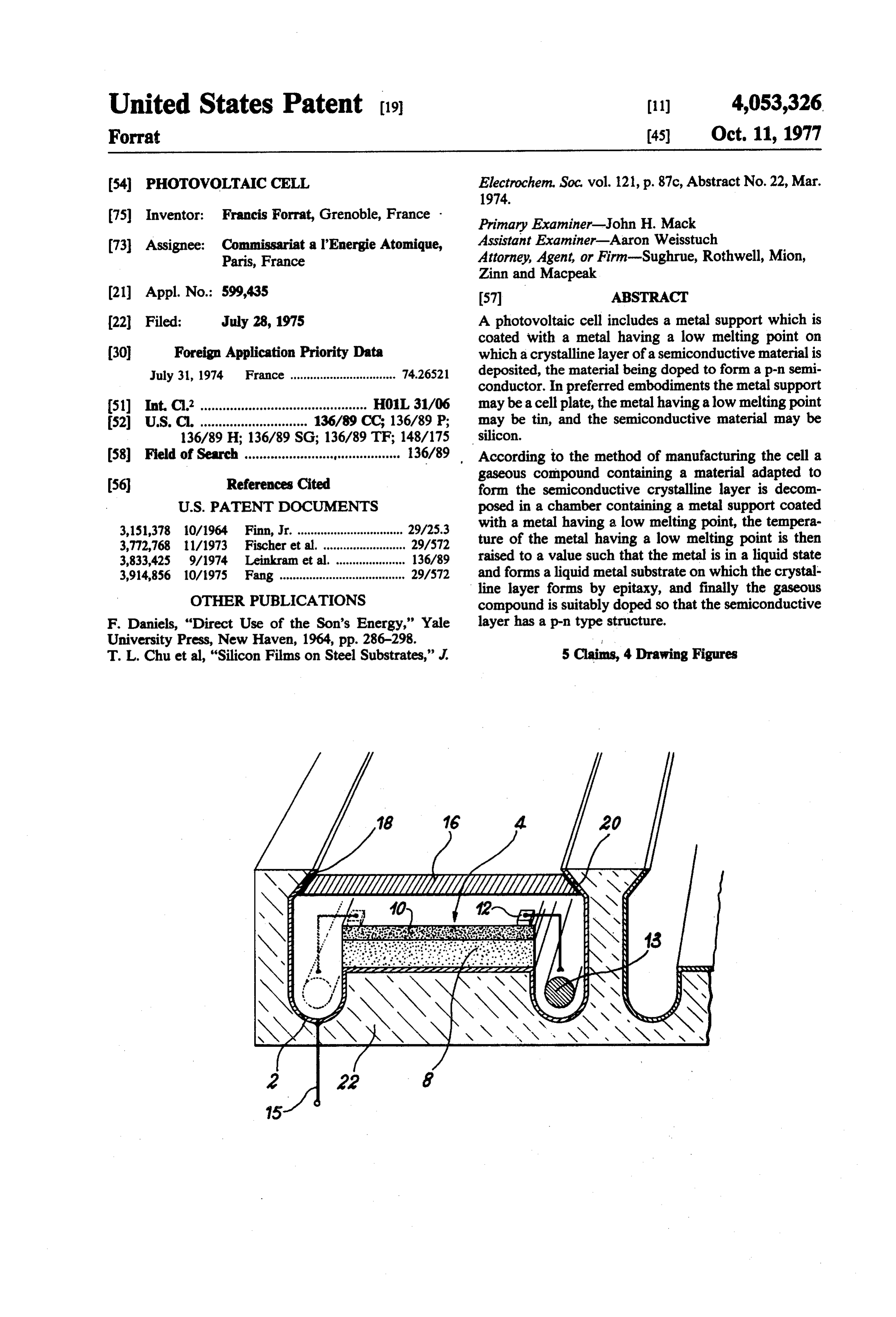
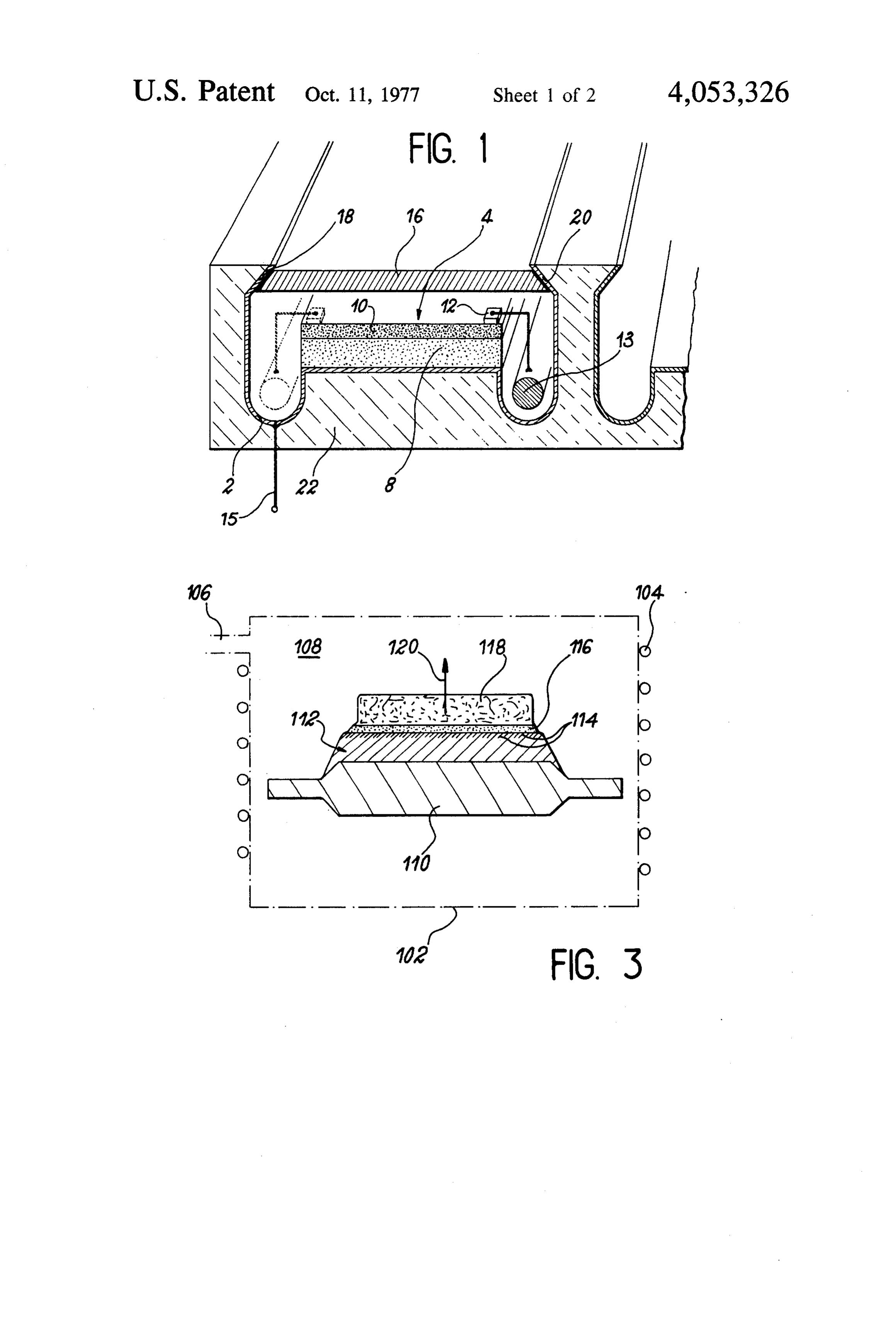
Turning now to FIG. 1, FIG. 1 shows a photovoltaic
To this end, according to the invention, use is made of cell comprising a tin-plated steel plate 2, the central part a metal plate coated with a metal having a low melting 20 of which bears a semiconductive layer 4 comprising e.g. point, to form the metal support on which the semi-con ap silicon layer 8 and an in silicon layer 10. On the top ductive layer is deposited. surface, connections 12 are connected to a collector 13 According to the invention there is provided a photo connected to an external connection (not shown); the voltaic cell, which comprises a metal support coated other connection 15 which has the opposite polarity with a metal having a low melting point on which a 25 from connection 12, is connected to plate 2. The photo crystalline layer of a semiconductive material is depos voltaic cell according to the invention can be closed at ited, the material being doped to form a p-n junction. its top by a glass plate 16 brazed to the plate at its ends
BRIEF DESCRIPTION OF THE DRAWINGS
18 and 20. An insulating support 22 completes the as sembly.
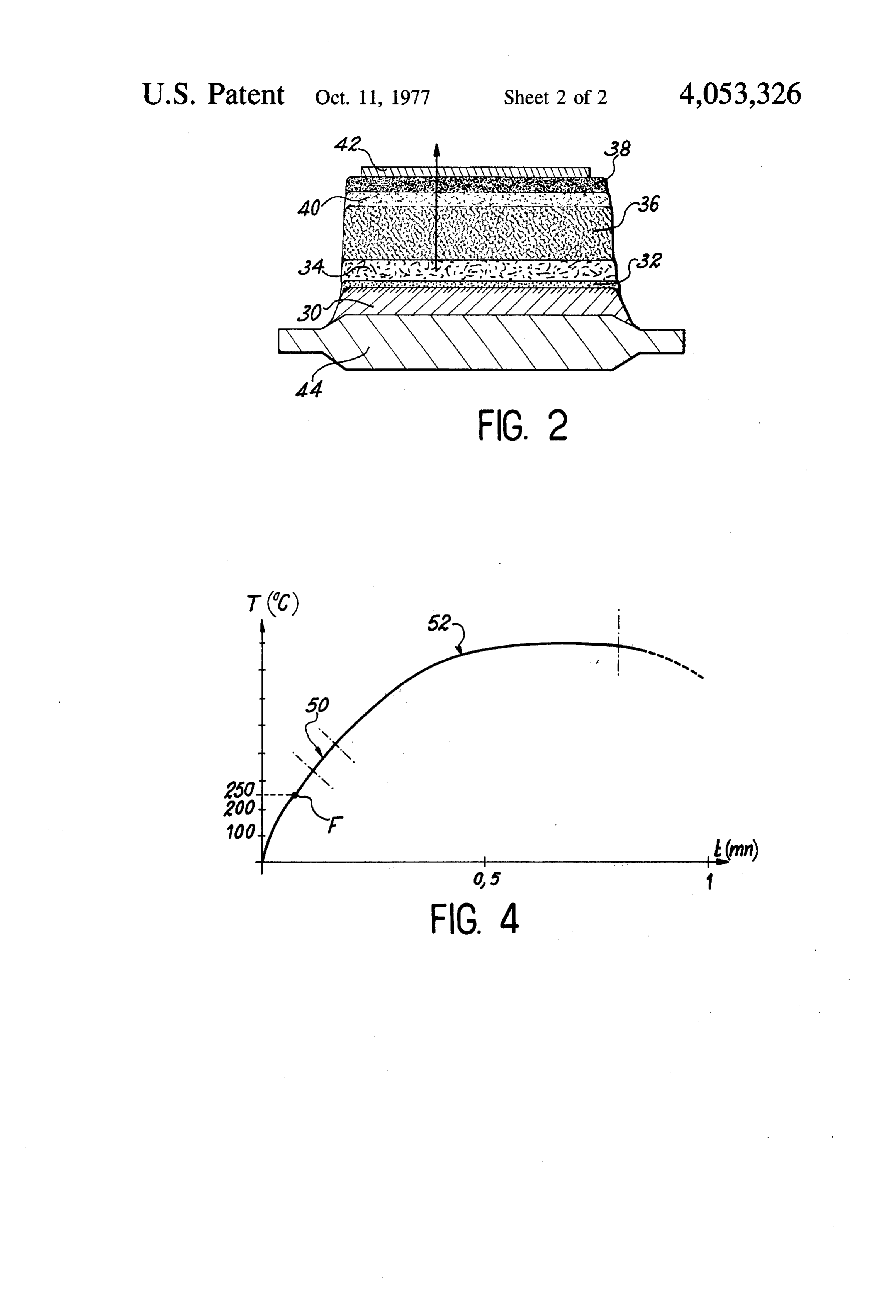
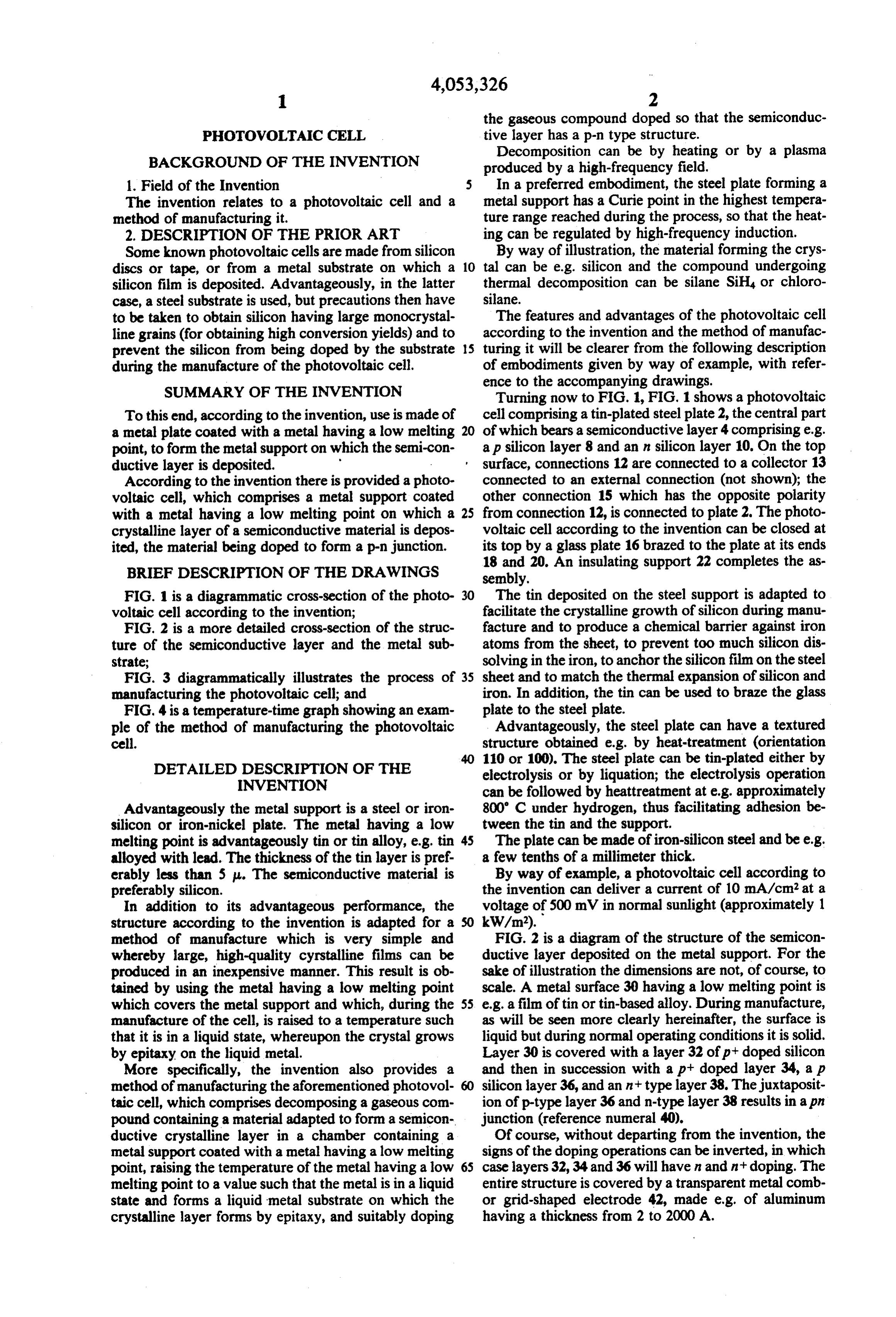
FIG. 1 is a diagrammatic cross-section of the photo 30 The tin deposited on the steel support is adapted to voltaic cell according to the invention; facilitate the crystalline growth of silicon during manu FIG. 2 is a more detailed cross-section of the struc facture and to produce a chemical barrier against iron ture of the semiconductive layer and the metal sub atoms from the sheet, to prevent too much silicon dis strate; solving in the iron, to anchor the silicon film on the steel FIG. 3 diagrammatically illustrates the process of 35 sheet and to match the thermal expansion of silicon and manufacturing the photovoltaic cell; and iron. In addition, the tin can be used to braze the glass FIG. 4 is a temperature-time graph showing an exam plate to the steel plate.
ple of the method of manufacturing the photovoltaic Advantageously, the steel plate can have a textured cell. structure obtained e.g. by heat-treatment (orientation
DETAILED DESCRIPTION OF THE
110 or 100). The steel plate can be tin-plated either by electrolysis or by liquation; the electrolysis operation
INVENTION can be followed by heatreatment at e.g. approximately Advantageously the metal support is a steel or iron 800' C under hydrogen, thus facilitating adhesion be silicon or iron-nickel plate. The metal having a low tween the tin and the support.
melting point is advantageously tin or tin alloy, e.g. tin 45 The plate can be made of iron-silicon steel and be e.g. alloyed with lead. The thickness of the tin layer is pref. a few tenths of a millimeter thick. erably less than 5 u. The semiconductive material is By way of example, a photovoltaic cell according to preferably silicon. the invention can deliver a current of 10 mA/cm2 at a In addition to its advantageous performance, the voltage of 500 mV in normal sunlight (approximately 1 structure according to the invention is adapted for a 50 kW/m2).
method of manufacture which is very simple and FIG. 2 is a diagram of the structure of the semicon whereby large, high-quality cyrstalline films can be ductive layer deposited on the metal support. For the produced in an inexpensive manner. This result is ob sake of illustration the dimensions are not, of course, to tained by using the metal having a low melting point scale. A metal surface 30 having a low melting point is which covers the metal support and which, during the 55 e.g. a film of tin or tin-based alloy. During manufacture, manufacture of the cell, is raised to a temperature such as will be seen more clearly hereinafter, the surface is that it is in a liquid state, whereupon the crystal grows liquid but during normal operating conditions it is solid. by epitaxy on the liquid metal. Layer 30 is covered with a layer 32 of p + doped silicon More specifically, the invention also provides a and then in succession with a pit doped layer 34, a p method of manufacturing the aforementioned photovol 60 silicon layer 36, and an int type layer 38. The juxtaposit taic cell, which comprises decomposing a gaseous com ion of p-type layer 36 and n-type layer 38 results in a pn pound containing a material adapted to form a semicon junction (reference numeral 40).
ductive crystalline layer in a chamber containing a Of course, without departing from the invention, the metal support coated with a metal having a low melting signs of the doping operations can be inverted, in which point, raising the temperature of the metal having a low 65 case layers 32,34 and 36 will have n and n + doping. The melting point to a value such that the metal is in a liquid entire structure is covered by a transparent metal comb state and forms a liquid metal substrate on which the or grid-shaped electrode 42, made e.g. of aluminum crystalline layer forms by epitaxy, and suitably doping having a thickness from 2 to 2000 A.
Page 5
FIG. 3 diagrammatically illustrates the method of following operations are performed, starting from a manufacturing the aforementioned photovoltaic cell. In commercial 3/10 10-plated iron tape comprising 2 ultin: FIG. 3, a chamber 102 is provided with heating means 1. embossing;
104 and an inlet 106 for injecting a gaseous compound 2. chemical scouring with zinc chloride ZnCl2; and into chamber 108, the compound containing the sub 3. insertion into an epitaxy furnace. stance to be deposited. A support 110 surmounted by a These three operations are performed on a conveying metal substrate 112 is disposed in the chamber. The machine.
temperature of substrate 112 is raised by heating means The power of the generator is increased until the 104 to a temperature such that the gaseous compound in O entire temperature is reached and stabilized to h 1' Cover the space 108 is decomposed by heating, producing a mate Next, the sheet being processed (for about 10 minutes). rial for forming the crystal, and such that the metal epitaxy. Next, desired structure is formed by conventional the heating power is reduced to ensure substrate 112 is liquefied at least on its surface. After abundant seeding of tin, so as to ensure adhesion. Next becoming liquid, substrate 112 produces nuclei 114 at its the following operations are performed: surface, resulting in the formation of a thin layer 116 15 4. transfer to a masking chamber;
which in turn forms a nucleus on which crystal 118 can 5. deposition of the collector by a conventional grow by epitaxy in direction 120. method; and
If the crystal-forming material is silicon, the thin layer 6. coating.
116 comprises a compact hexagonal arrangement, in the Of course, the compound can be decomposed by a case of non-textured steel. As soon as the silicon atoms 20 plasma produced in a gas at a pressure between e.g. 1 are deposited, they gather around the first deposited and 100 Torr, using a high-frequency field having a atoms. As soon as the first layer is deposited on the frequency between e.g. kHz and MHz. The metal sub liquid metal, growth occurs by conventional epitaxy on strate can be heated by HF induction or conduction. the base assembly. In order to increase the crystal depo claim:
sition rate, the operating temperature can be increased 25 1. A photovoltaic cell comprising a steel plate having above the decomposition point of silane. a textured structure coated with tin and a crystalline The silicon crystal can be doped by mixing the silane layer of a semiconductive material deposited thereon with doping agents such as boron, to obtain type pit or p-n with the semiconductive material being doped to form a p doping (ph doping corresponds to a concentration of 30 decomposing junction, said photovoltaic cell being produced by about 1016 atoms of doping agent per cm, and type p rial which forms a gaseous compound containing a mate doping to about 1015 atoms/cm3). To obtain type in dop a chamber containing the semiconductive crystalline layer in ing, the silane can be mixed with phosphorus. said steel plate having a textured surface coated with the
Advantageously the metal support is a liquid film of a the tin is raised to a temperaturetin, wherein the temperature of metal having a Curie point corresponding to the highest 35 the liquid state and forms a liquid tin such that the tin is in temperature range in the method of operation, so as to the crystalline layer forms by epitaxy,substrate on which and wherein the ensure automatic control. For example, the metal sup gaseous compound is suitably doped so that the semi port can be made of a steel sheet having a Curie point conductive layer has the p-n structure. between 600' and 1000 C. In this case the temperature 2. A photovoltaic cell comprising a steel, iron-silicon time diagram characterizing the thermal program in or iron-nickel support coated with tin or a tin alloy and posed on the system can be of the kind illustrated in a crystalline layer of a semiconductive layer deposited FIG. 4, where the time is shown as the abscissa and the thereon with the semiconductive material being doped temperature as the ordinate. to form a p-n junction, said photovoltaic cell being First, the temperature is raised to a point F where the produced by decomposing a gaseous compound con metal forming substrate 30 melts. The temperature con taining a material which forms the semiconductive crys tinues to increase to a range 50 where the layer forming talline layer in a chamber containing said metal support the nucleus 32 is deposited. Beyond this range, crystal coated with the tin or tin alloy, wherein the temperature formation and growth by epitaxy is observed in the of the tin or tin alloy is raised to a temperature such that entire region 52, possibly accompanied by the formation SO the tin or tin alloy is in the liquid state and forms a tin or of doped Sip+, p and n regions. When the last Sin layer forms tin alloy metal substrate on which the crystalline layer has been deposited, the temperature of the layer of suitablybydoped epitaxy, and wherein the gaseous compound is so that the semiconductive layer has the liquid tin is lowered to about 232 C, to prevent stress p-n structure, the melting point of said tin or tin alloy on the silicon. The duration of the process can be e.g. of being such that during said decomposing the tin or tin the order of 10 minutes. alloy will melt into the liquid state and crystalline
The method can be used to obtain high-quality sili growth will be by epitaxy thereon.
con; it does not dislocate the crystal during the manu 3. The photovoltaic cell according to claim 2, facture of the entire structure, which is manufactured wherein said tin alloy is a tin-lead alloy. entirely "in situ'; the method of manufacture is eco 4. The photovoltaic cell according to claim 2, nomic; and large continuously-moving surfaces can be 60 wherein said semiconductive material is silicon. processed without using control devices. 5. A photovoltaic cell comprising a steel support For example, the aforementioned method can be used coated with tin and a crystalline layer of silicon depos to produce photovoltaic cells measuring 2 X 500 cm ited on said tin-coated steel support with the silicon and adapted to form solar batteries, the cells being being doped to form a p-n junction.
mounted in parallel groups on insulating panels. The s s
Provenance
- Collection
- Cited prior art
- Original PDF
- patentimages.storage.googleapis.com →
- Filed
- 1975-07-28
- Pages
- 5
- Method
- pdftotext (the PDF's own text layer) + pdftoppm 300dpi page scans
- Source
- Google Patents bibliographic record
- Granted
- 1977-10-11
- Inventors
- Francis Forrat; Commissariat a lEnergie Atomique CEA
- Transcribed from
- patentimages.storage.googleapis.com →