patent · US3925212
Device for solar energy conversion by photo-electrolytic decomposition of water
9 December 1975
Page 1 — bibliographic record
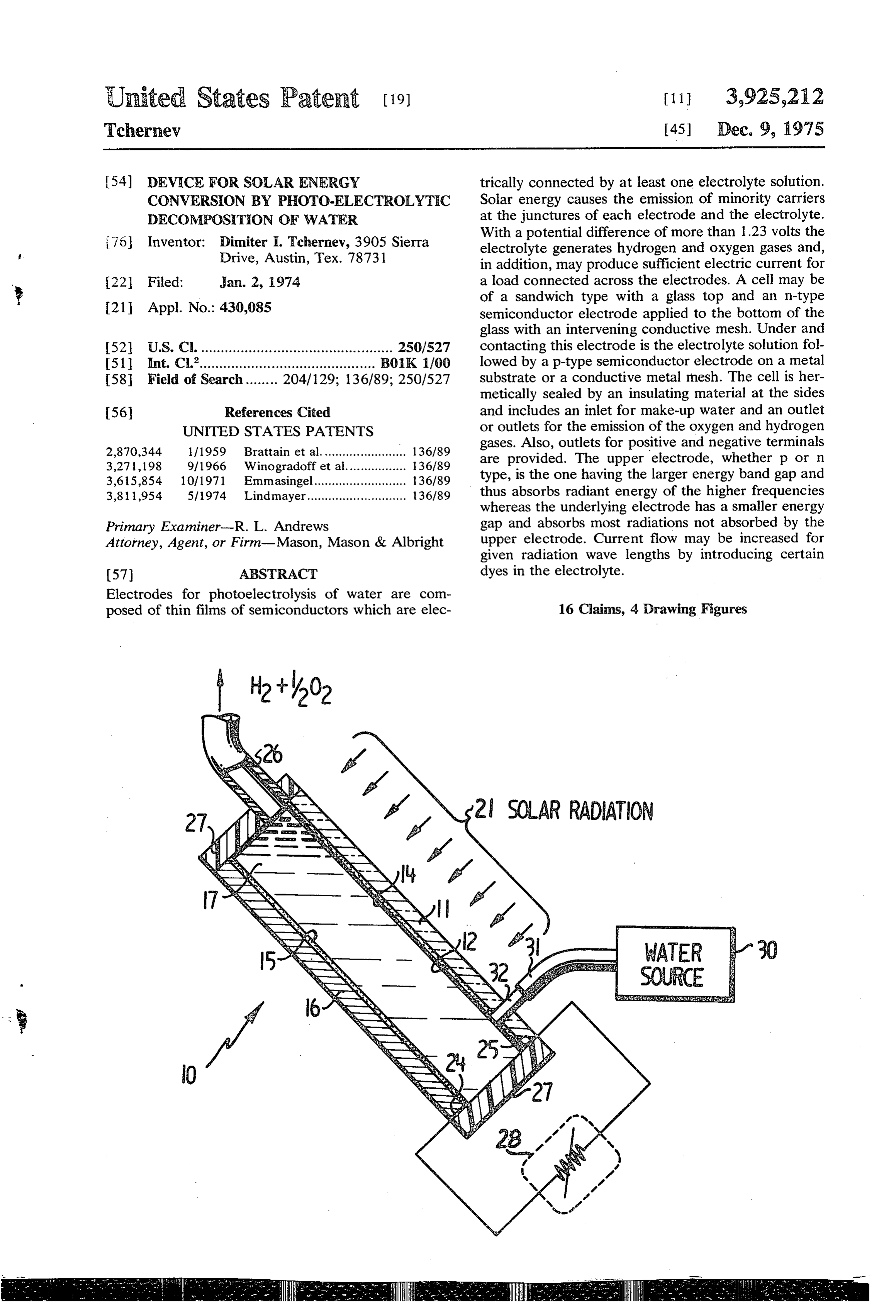
United States Patent (19) 11 3,925,212 Tcherhev (45) Dec. 9, 1975 54 DEVICE FOR SOLAR ENERGY trically connected by at least one electrolyte solution. CONVERSION BY PHOTO-ELECTROLYTC Solar energy causes the emission of minority carriers DECOMPOSITION OF WATER at the junctures of each electrode and the electrolyte. if 6 Inventor: Dimiter I. Tchernev, 3905 Sierra With a potential difference of more than 1.23 volts the electrolyte generates hydrogen and oxygen gases and,
Drive, Austin, Tex. 78731 in addition, may produce sufficient electric current for 22 Filed: Jana. 2, 974 a load connected across the electrodes. A cell may be of a sandwich type with a glass top and an n-type 21 Appl. No.: 430,085 semiconductor electrode applied to the bottom of the glass with an intervening conductive mesh. Under and
I52) U.S.C. ................................................ 250/527 contacting this electrode is the electrolyte solution fol I51 int. Cl.’............................................ B0K 1100 lowed by a p-type semiconductor electrode on a metal 58 Field of Search ........ 204/129; 136/89; 250/527 substrate or a conductive metal mesh. The cell is her metically sealed by an insulating material at the sides 56) References Cited and includes an inlet for make-up water and an outlet UNITED STATES PATENTS or outlets for the emission of the oxygen and hydrogen 2,870,344 l/1959 Brattain et al......................... 136/89 gases. Also, outlets for positive and negative terminals 3,271,198 9/1966 Winogradoff et al... ... 136189 are provided. The upper electrode, whether p or n 3,615,854 10/1971 Emmasingel............ ... 136/89 type, is the one having the larger energy band gap and 3,811,954 5/1974 Lindmayer............................ 136/89 thus absorbs radiant energy of the higher frequencies whereas the underlying electrode has a smaller energy
Primary Examiner-R. L. Andrews gap and absorbs most radiations not absorbed by the Attorney, Agent, or Firm-Mason, Mason & Albright upper electrode. Current flow may be increased for given radiation wave lengths by introducing certain 57 ABSTRACT dyes in the electrolyte.
Electrodes for photoelectrolysis of water are com posed of thin films of semiconductors which are elec 16 Claims, 4 Drawing Figures
Page 2
Drawing sheet — no readable text.
Page 3
Drawing sheet — no readable text.
Page 4
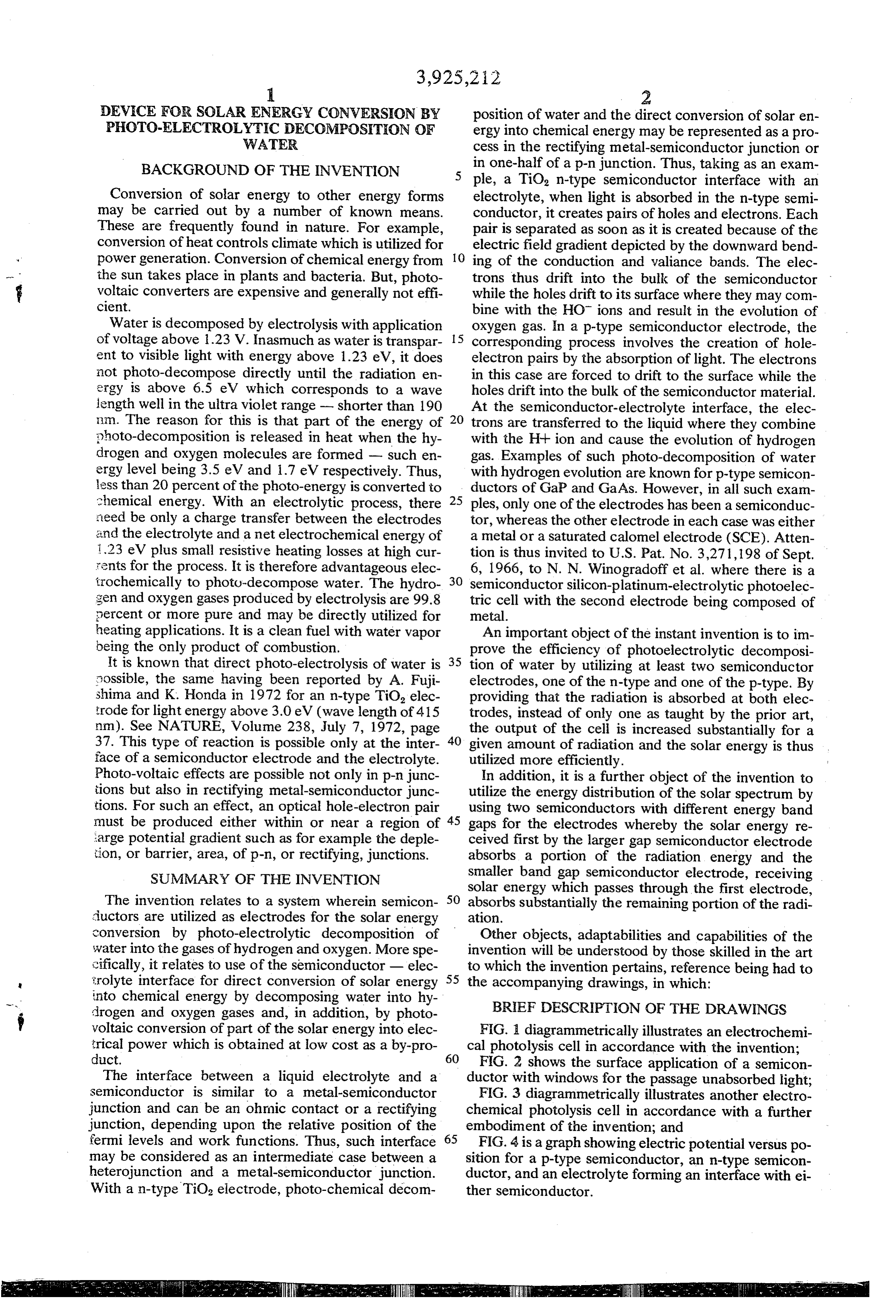
DEVICE FOR SOLAR ENERGY CONVERSION BY position of water and the direct conversion of solar en PHOTO-ELECTROLYTIC DECOMPOSITON OF ergy into chemical energy may be represented as a pro WATER cess in the rectifying metal-semiconductor junction or BACKGROUND OF THE INVENTION in one-half of a p-n junction. Thus, taking as an exam ple, a TiO, n-type semiconductor interface with an
Conversion of solar energy to other energy forms electrolyte, when light is absorbed in the n-type semi may be carried out by a number of known means. conductor, it creates pairs of holes and electrons. Each These are frequently found in nature. For example, pair is separated as soon as it is created because of the conversion of heat controls climate which is utilized for electric field gradient depicted by the downward bend power generation. Conversion of chemical energy from 10 ing of the conduction and valiance bands. The elec the sun takes place in plants and bacteria. But, photo trons thus drift into the bulk of the semiconductor voltaic converters are expensive and generally not effi while the holes drift to its surface where they may com Cient. bine with the HOT ions and result in the evolution of Water is decomposed by electrolysis with application oxygen gas. In a p-type semiconductor electrode, the of voltage above 1.23 V. Inasmuch as water is transpar 15 corresponding process involves the creation of hole ent to visible light with energy above 1.23 eV, it does electron pairs by the absorption of light. The electrons not photo-decompose directly until the radiation en in this case are forced to drift to the surface while the ergy is above 6.5 eV which corresponds to a wave holes drift into the bulk of the semiconductor material. length well in the ultra violet range - shorter than 190 At the semiconductor-electrolyte interface, the elec nm. The reason for this is that part of the energy of 20 trons are transferred to the liquid where they combine photo-decomposition is released in heat when the hy with the H+ ion and cause the evolution of hydrogen drogen and oxygen molecules are formed - such en gas. Examples of such photo-decomposition of water ergy level being 3.5 eV and 1.7 eV respectively. Thus, with hydrogen evolution are known for p-type semicon less than 20 percent of the photo-energy is converted to ductors of Gap and GaAs. However, in all such exam chemical energy. With an electrolytic process, there 25 ples, only one of the electrodes has been a semiconduc aeed be only a charge transfer between the electrodes tor, whereas the other electrode in each case was either and the electrolyte and a net electrochemical energy of a metal or a saturated calomel electrode (SCE). Atten i.23 eV plus small resistive heating losses at high cur tion is thus invited to U.S. Pat. No. 3,271,198 of Sept. rents for the process. It is therefore advantageous elec 6, 1966, to N. N. Winogradoff et al. where there is a trochemically to photo-decompose water. The hydro 30 semiconductor silicon-platinum-electrolytic photoelec gen and oxygen gases produced by electrolysis are 99.8 tric cell with the second electrode being composed of percent or more pure and may be directly utilized for metal.
heating applications. It is a clean fuel with water vapor An important object of the instant invention is to im being the only product of combustion. prove the efficiency of photoelectrolytic decomposi It is known that direct photo-electrolysis of water is 35 tion of water by utilizing at least two semiconductor ossible, the same having been reported by A. Fuji electrodes, one of the n-type and one of the p-type. By shima and K. Honda in 1972 for an n-type TiO, elec providing that the radiation is absorbed at both elec trode for light energy above 3.0 eV (wave length of 415 trodes, instead of only one as taught by the prior art, nm). See NATURE, Volume 238, July 7, 1972, page the output of the cell is increased substantially for a 37. This type of reaction is possible only at the inter 40 given amount of radiation and the solar energy is thus face of a semiconductor electrode and the electrolyte. utilized more efficiently.
Photo-voltaic effects are possible not only in p-n junc In addition, it is a further object of the invention to tions but also in rectifying metal-semiconductor junc utilize the energy distribution of the solar spectrum by tions. For such an effect, an optical hole-electron pair using two semiconductors with different energy band must be produced either within or near a region of 45 gaps for the electrodes whereby the solar energy re arge potential gradient such as for example the deple ceived first by the larger gap semiconductor electrode tion, or barrier, area, of p-n, or rectifying, junctions. absorbs a portion of the radiation energy and the SUMMARY OF THE INVENTION smaller band gap semiconductor electrode, receiving solar energy which passes through the first electrode,
The invention relates to a system wherein semicon 50 absorbs substantially the remaining portion of the radi ductors are utilized as electrodes for the solar energy aton.
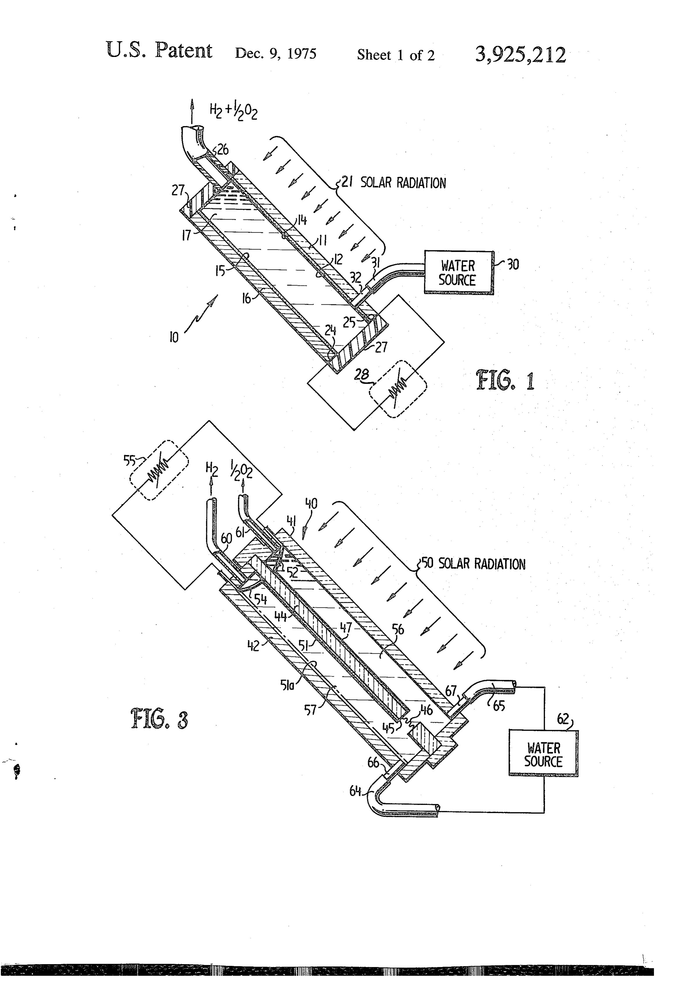
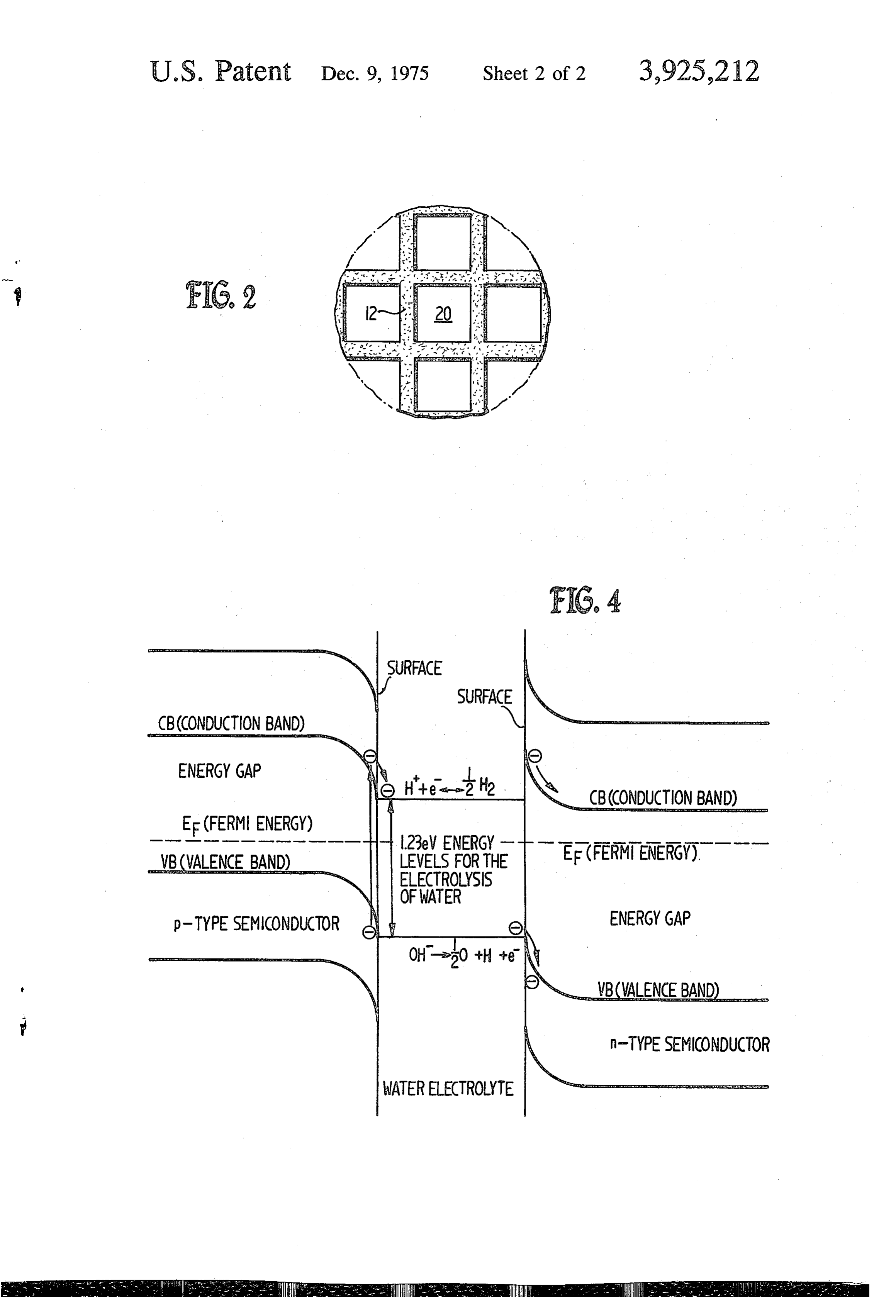
conversion by photo-electrolytic decomposition of Other objects, adaptabilities and capabilities of the water into the gases of hydrogen and oxygen. More spe invention will be understood by those skilled in the art cifically, it relates to use of the semiconductor -elec to which the invention pertains, reference being had to irolyte interface for direct conversion of solar energy 55 the accompanying drawings, in which: into chemical energy by decomposing water into hy irogen and oxygen gases and, in addition, by photo BRIEF OESCRIPTION OF THE DRAWINGS voltaic conversion of part of the solar energy into elec FIG. diagrammetrically illustrates an electrochemi trical power which is obtained at low cost as a by-pro cal photolysis cell in accordance with the invention; duct. 60 FIG. 2 shows the surface application of a semicon The interface between a liquid electrolyte and a ductor with windows for the passage unabsorbed light; semiconductor is similar to a metal-semiconductor FIG. 3 diagrammetrically illustrates another electro junction and can be an ohmic contact or a rectifying chemical photolysis cell in accordance with a further junction, depending upon the relative position of the embodiment of the invention; and fermi levels and work functions. Thus, such interface 65 FIG. 4 is a graph showing electric potential versus po may be considered as an intermediate case between a sition for a p-type semiconductor, an n-type semicon heterojunction and a metal-semiconductor junction. ductor, and an electrolyte forming an interface with ei With a n-type TiO, electrode, photo-chemical decom ther semiconductor.
Page 5
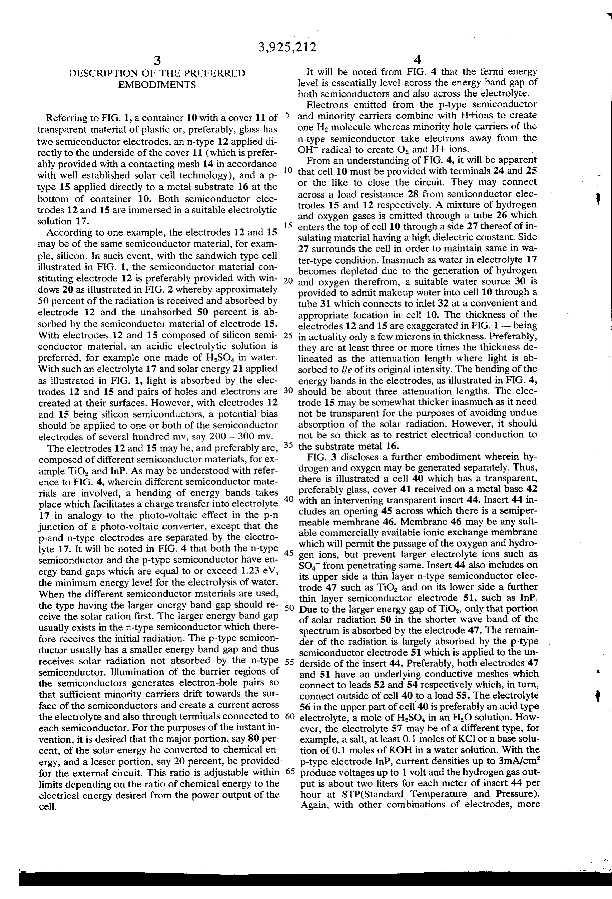
DESCRIPTION OF THE PREFERRED It will be noted from FIG. 4 that the fermi energy EMBODIMENTS level is essentially level across the energy band gap of both semiconductors and also across the electrolyte.
Electrons emitted from the p-type semiconductor
Referring to FIG. 1, a container 10 with a cover 11 of 5 and minority carriers combine with H-ions to create transparent material of plastic or, preferably, glass has one H2 molecule whereas minority hole carriers of the two semiconductor electrodes, an n-type 12 applied di n-type semiconductor take electrons away from the rectly to the underside of the cover 11 (which is prefer OHFromradical to create O and HH- ions. an understanding of FIG. 4, it will be apparent ably provided with a contacting mesh 14 in accordance O that cell with well established solar cell technology), and a p or the like 10 must be provided with terminals 24 and 25 type 15 applied directly to a metal substrate 16 at the across a loadtoresistance close the circuit. They may connect 28 from semiconductor elec bottom of container 10. Both semiconductor elec trodes 12 and 15 are immersed in a suitable electrolytic trodes and 15 and 12 respectively. A mixture of hydrogen oxygen gases is emitted through a tube 26 which solution 17. 15 enters the top of cell 10 through a side 27 thereof of in According to one example, the electrodes 12 and 15 sulating material having a high dielectric constant. Side may be of the same semiconductor material, for exam 27 surrounds the cell in order to maintain same in wa ple, silicon. In such event, with the sandwich type cell ter-type condition. Inasmuch as water in electrolyte 17 illustrated in FIG. 1, the semiconductor material con becomes depleted due to the generation of hydrogen stituting electrode 12 is preferably provided with win 20 and oxygen therefrom, a suitable water source 30 is dows 20 as illustrated in FIG. 2 whereby approximately provided to admit makeup water into cell 10 through a 50 percent of the radiation is received and absorbed by tube 31 which connects to inlet 32 at a convenient and electrode 12 and the unabsorbed 50 percent is ab appropriate location in cell 10. The thickness of the sorbed by the semiconductor material of electrode 15. electrodes 12 and 15 are exaggerated in FIG. 1 - being With electrodes 12 and 15 composed of silicon semi 25 in actuality only a few microns in thickness. Preferably, conductor material, an acidic electrolytic solution is they are at least three or more times the thickness de preferred, for example one made of HSO in water. lineated as the attenuation length where light is ab With such an electrolyte 17 and solar energy 21 applied sorbed to life of its original intensity. The bending of the as illustrated in FIG. 1, light is absorbed by the elec energy bands in the electrodes, as illustrated in FIG. 4, trodes 12 and 15 and pairs of holes and electrons are 30 should be about three attenuation lengths. The elec created at their surfaces. However, with electrodes 12 trode 15 may be somewhat thicker inasmuch as it need and 15 being silicon semiconductors, a potential bias not be transparent for the purposes of avoiding undue should be applied to one or both of the semiconductor absorption of the solar radiation. However, it should electrodes of several hundred mv, say 200 - 300 mV. 35 not be so thick as to restrict electrical conduction to The electrodes 12 and 15 may be, and preferably are, the substrate metal 16.
composed of different semiconductor materials, for ex drogen FIG. 3 discloses a further embodiment wherein hy ample TiO, and InP. As may be understood with refer there isand oxygen may be generated separately. Thus, illustrated a cell 40 which has a transparent, ence to FIG. 4, wherein different semiconductor mate rials are involved, a bending of energy bands takes preferably glass, cover 41 received on a metal base 42 place which facilitates a charge transfer into electrolyte 40 with an intervening transparent insert 44. Insert 44 in 17 in analogy to the photo-voltaic effect in the p-n cludes anmembrane opening 45 across which there is a semiper junction of a photo-voltaic converter, except that the meable 46. Membrane 46 may be any suit p-and n-type electrodes are separated by the electro which will permit the passageionic able commercially available
exchange membrane the oxygen and hydro lyte 17. It will be noted in FIG. 4 that both the n-type 45 gen ions, but prevent larger electrolyte semiconductor and the p-type semiconductor have en SO, from penetrating same. Insert 44 alsoions such as includes on ergy band gaps which are equal to or exceed 1.23 eV, its upper side a thin layer n-type semiconductor elec the minimum energy level for the electrolysis of water. trode 47 such as TiO, and on its lower side a further When the different semiconductor materials are used, the type having the larger energy band gap should re 50 thin Due layer semiconductor electrode 51, such as InP.
to the larger energy gap of TiO, only that portion ceive the solar ration first. The larger energy band gap of solar radiation 50 in the shorter wave band of the usually exists in the n-type semiconductor which there spectrum is absorbed by the electrode 47. The remain fore receives the initial radiation. The p-type semicon der of the radiation is largely absorbed by the p-type ductor usually has a smaller energy band gap and thus semiconductor electrode 51 which is applied to the un receives solar radiation not absorbed by the n-type 55 derside of the insert 44. Preferably, both electrodes 47 semiconductor. Illumination of the barrier regions of and 51 have an underlying conductive meshes which the semiconductors generates electron-hole pairs so connect to leads 52 and 54 respectively which, in turn, that sufficient minority carriers drift towards the sur connect outside of cell 40 to a load 55. The electrolyte face of the semiconductors and create a current across 56 in the upper part of cell 40 is preferably an acid type the electrolyte and also through terminals connected to 60 electrolyte, a mole of HSO in an HO solution. How each semiconductor. For the purposes of the instant in ever, the electrolyte 57 may be of a different type, for vention, it is desired that the major portion, say 80 per example, a salt, at least 0.1 moles of KCl or a base solu cent, of the solar energy be converted to chemical en tion of 0.1 moles of KOH in a water solution. With the ergy, and a lesser portion, say 20 percent, be provided p-type electrode InP, current densities up to 3mA/cm for the external circuit. This ratio is adjustable within 65 produce voltages up to 1 volt and the hydrogen gas out limits depending on the ratio of chemical energy to the put is about two liters for each meter of insert 44 per electrical energy desired from the power output of the hour at STP(Standard Temperature and Pressure). cell. Again, with other combinations of electrodes, more
Page 6
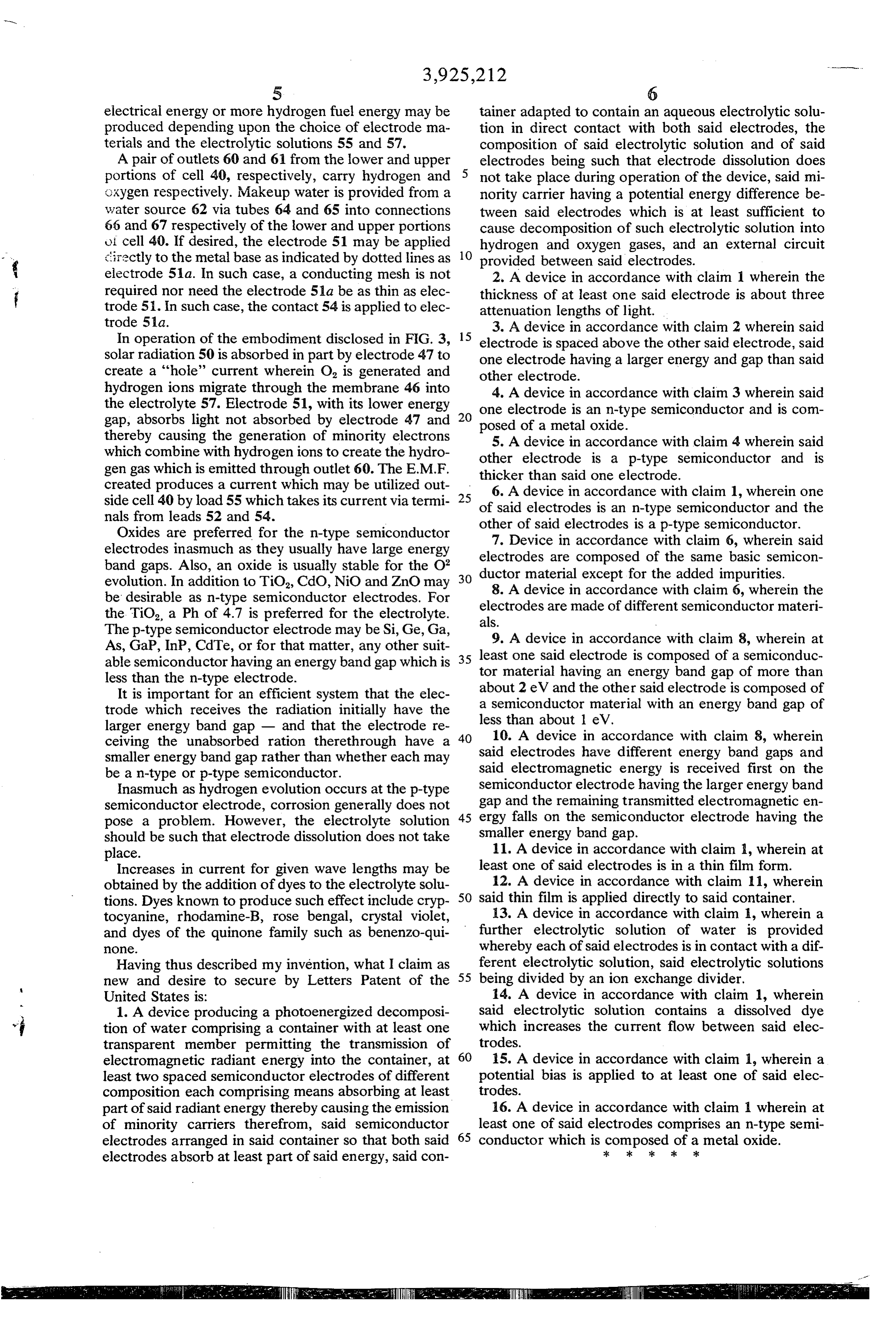
S 6 electrical energy or more hydrogen fuel energy may be tainer adapted to contain an aqueous electrolytic solu produced depending upon the choice of electrode ma tion in direct contact with both said electrodes, the terials and the electrolytic solutions 55 and 57. composition of said electrolytic solution and of said A pair of outlets 60 and 61 from the lower and upper electrodes being such that electrode dissolution does portions of cell 40, respectively, carry hydrogen and 5 not take place during operation of the device, said mi 3Xygen respectively. Makeup water is provided from a nority carrier having a potential energy difference be water source 62 via tubes 64 and 65 into connections tween said electrodes which is at least sufficient to 66 and 67 respectively of the lower and upper portions cause decomposition of such electrolytic solution into of cell 40. If desired, the electrode 51 may be applied hydrogen and oxygen gases, and an external circuit tirectly to the metal base as indicated by dotted lines as 10 provided between said electrodes. electrode 51a. In such case, a conducting mesh is not 2. A device in accordance with claim 1 wherein the required nor need the electrode 51a be as thin as elec thickness of at least one said electrode is about three trode 51. In such case, the contact 54 is applied to elec attenuation lengths of light. trode 5 a. 3. A device in accordance with claim 2 wherein said In operation of the embodiment disclosed in FIG. 3, 15 electrode is spaced above the other said electrode, said solar radiation 50 is absorbed in part by electrode 47 to one electrode having a larger energy and gap than said create a "hole' current wherein O, is generated and other electrode.
hydrogen ions migrate through the membrane 46 into 4. A device in accordance with claim 3 wherein said the electrolyte 57. Electrode 51, with its lower energy one electrode is an n-type semiconductor and is com gap, absorbs light not absorbed by electrode 47 and 20 thereby causing the generation of minority electrons posed of a metal oxide.
5. A device in accordance with claim 4 wherein said which combine with hydrogen ions to create the hydro other electrode is a p-type semiconductor and is gen gas which is emitted through outlet 60. The E.M.F. thicker than said one electrode.
created produces a current which may be utilized out side cell 40 by load 55 which takes its current via termi- 25 of6.said
A device in accordance with claim 1, wherein one electrodes is an n-type semiconductor and the nals from leads 52 and 54.
Oxides are preferred for the n-type semiconductor other of said electrodes is a p-type semiconductor. 7. Device in accordance with claim 6, wherein said electrodes inasmuch as they usually have large energy electrodes are composed of the same basic semicon band gaps. Also, an oxide is usually stable for the O evolution. In addition to TiO, CdC), NiO and ZnO may 30 8. A device in except ductor material for the added impurities.
accordance with claim 6, wherein the be desirable as n-type semiconductor electrodes. For electrodes are made of different semiconductor materi the TiO, a Ph of 4.7 is preferred for the electrolyte. als.
The p-type semiconductor electrode may be Si, Ge, Ga, 9. A device in accordance with claim 8, wherein at As, GaP, InP, CdTe, or for that matter, any other suit least one said electrode is composed of a semiconduc able semiconductor having an energy bandgap which is 35 tor material having an energy band gap of more than less than the n-type electrode.
It is important for an efficient system that the elec about 2 eV and the other said electrode is composed of trode which receives the radiation initially have the less a semiconductor material with an energy band gap of larger energy band gap - and that the electrode re than about 1 eV.
ceiving the unabsorbed ration therethrough have a 40 10. A device in accordance with claim 8, wherein smaller energy band gap rather than whether each may said electrodes have different energy band gaps and be a n-type or p-type semiconductor. said electromagnetic energy is received first on the Inasmuch as hydrogen evolution occurs at the p-type semiconductor electrode having the larger energy band semiconductor electrode, corrosion generally does not gap and the remaining transmitted electromagnetic en pose a problem. However, the electrolyte solution 45 ergy falls on the semiconductor electrode having the should be such that electrode dissolution does not take smaller energy band gap.
place. 11. A device in accordance with claim , wherein at Increases in current for given wave lengths may be least one of said electrodes is in a thin film form. obtained by the addition of dyes to the electrolyte solu 12. A device in accordance with claim 1, wherein tions. Dyes known to produce such effect include cryp- 50 said thin film is applied directly to said container. tocyanine, rhodamine-B, rose bengal, crystal violet, 13. A device in accordance with claim I, wherein a and dyes of the quinone family such as benenzo-qui further electrolytic solution of water is provided Oc. whereby each of said electrodes is in contact with a dif Having thus described my invention, what I claim as ferent electrolytic solution, said electrolytic solutions new and desire to secure by Letters Patent of the 55 being divided by an ion exchange divider. United States is: 14. A device in accordance with claim 1, wherein 1. A device producing a photoenergized decomposi said electrolytic solution contains a dissolved dye tion of water comprising a container with at least one which increases the current flow between said elec transparent member permitting the transmission of trodes.
electromagnetic radiant energy into the container, at 60 15. A device in accordance with claim 1, wherein a least two spaced semiconductor electrodes of different potential bias is applied to at least one of said elec composition each comprising means absorbing at least trodes.
part of said radiant energy thereby causing the emission 16. A device in accordance with claim wherein at of minority carriers therefrom, said semiconductor least one of said electrodes comprises an n-type semi electrodes arranged in said container so that both said 65 conductor which is composed of ak metal oxide. electrodes absorb at least part of said energy, said con K ck :: ck
Provenance
- Collection
- Cited prior art
- Original PDF
- patentimages.storage.googleapis.com →
- Filed
- 1974-01-02
- Pages
- 6
- Method
- pdftotext (the PDF's own text layer) + pdftoppm 300dpi page scans
- Source
- Google Patents bibliographic record
- Granted
- 1975-12-09
- Inventors
- Dimiter I Tchernev
- Transcribed from
- patentimages.storage.googleapis.com →