patent · US3875456
Multi-color semiconductor lamp
1 April 1975
Page 1 — bibliographic record
United States Patent (19) [11] 3,875,456 Kano et al. (45) Apr. 1, 1975 54) MULTI-COLOR SEMCONDUCTOR LAMP OTHER PUBLICATIONS 75) Inventors: Tsuyoshi Kano; Tadashi Saitoh; Van Vitert, et al., "Infra-Red Stimulable Rare Earth Atsushi Suzuki; Teruki Suzuki; Oxy-Halide Phosphors; Their Synthesis, Properties Shigekazu Minagawa; Yoshiro and Applications,' Pergamon Press, pg. 381-390, Otomo, all of Tokyo, Japan 1969.
(73) Assignee: Hitachi, Ltd., Tokyo, Japan Jacobus et al., “Visible Light Emitting Diodes,' IBM Technical Disclosure Bulletin, Vol. 10, No. 8, Jan.
22 Filed: Apr. 4, 1973 1968, p. 1120.
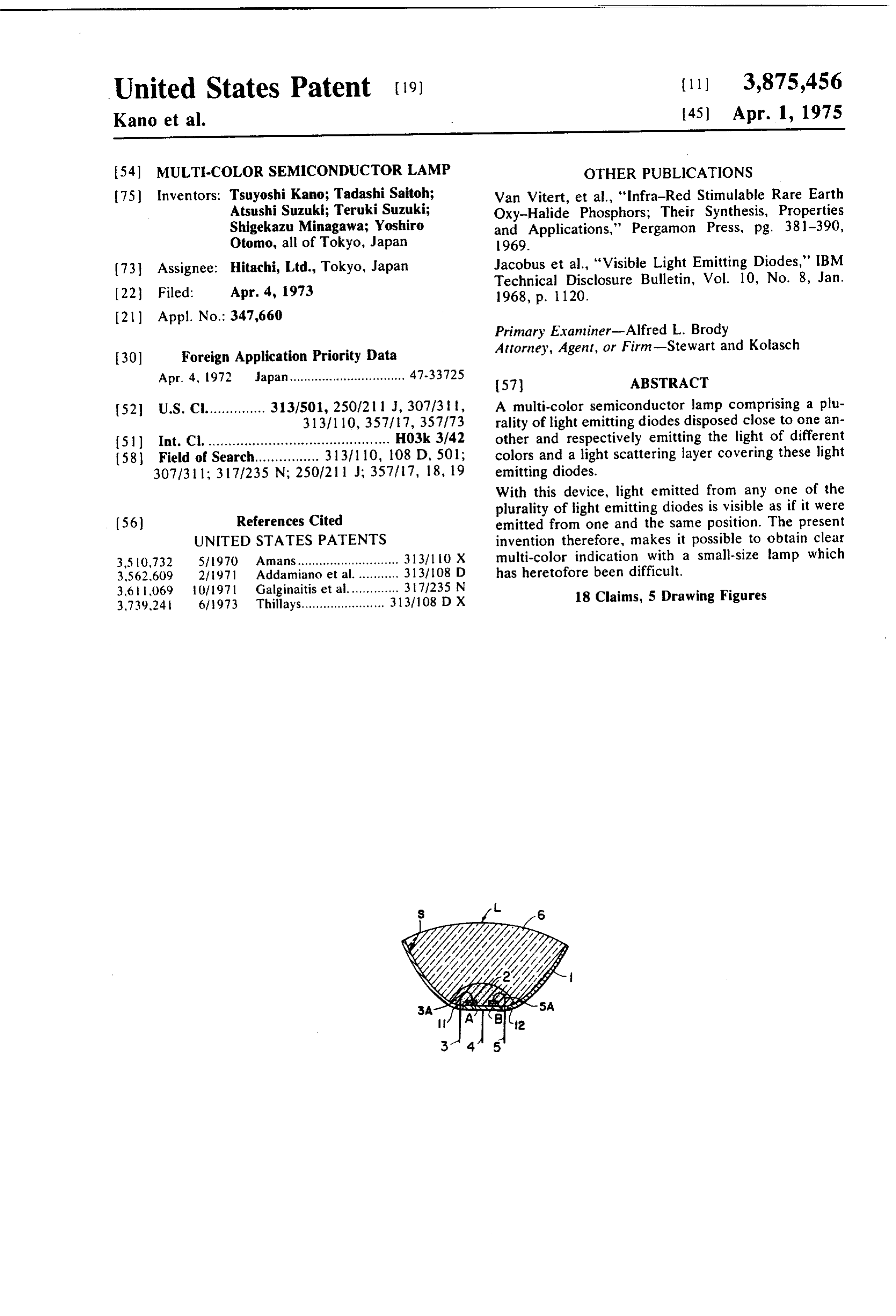
Primary Examiner-Alfred L. Brody (30) Foreign Application Priority Data Attorney, Agent, or Firm-Stewart and Kolasch Apr. 4, 1972 Japan................................ 47.33725 57) ABSTRACT 52 U.S. Cl............... 3131501, 250/21 1 J, 307/3, A multi-color semiconductor lamp comprising a plu 313/110,357/7, 357f73 rality of light emitting diodes disposed close to one an 5) Int. Cl. ............................................. H03k 3/42 other and respectively emitting the light of different 58) Field of Search................ 31311 10, 108 D, 501; colors and a light scattering layer covering these light 307/31; 31 7/235 N; 250/21 1 J; 357/7, 18, 19 emitting diodes.
With this device, light emitted from any one of the plurality of light emitting diodes is visible as if it were 56) References Cited emitted from one and the same position. The present UNITED STATES PATENTS invention therefore, makes it possible to obtain clear 3,50,732 51970 Amans............................ 313/1 O X multi-color indication with a small-size lamp which 3,562,609 21971 Addamiano et al............ 313/08 D has heretofore been difficult. 3,61 1,069 10/1971 Galginaitis et al.............. 37/235 N 18 Claims, 5 Drawing Figures 3,739,241 6/1973 Thillays....................... 313/108 D X
Page 2
Drawing sheet — no readable text.
Page 3
MULTI-COLOR SEMICONDUCTOR LAMP and nevertheless permits to emit light in clear and dis tinct colors.
BACKGROUND OF THE INVENTION
SUMMARY OF THE INVENTION
l, Field of the Invention
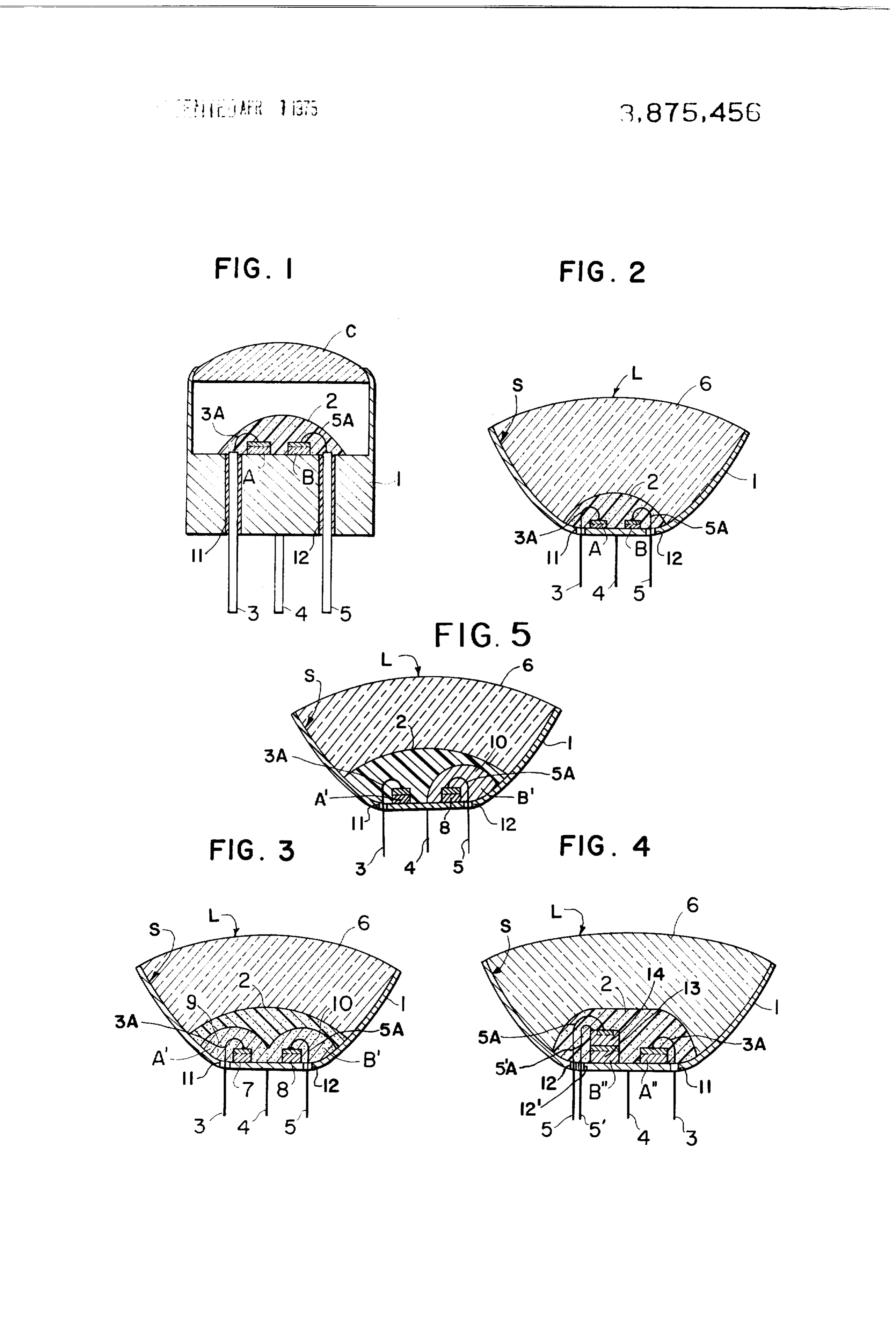
This invention relates to semiconductor lamps and s According to the invention, a plurality of light more particularly, to multi-color semiconductor lamps emitting diodes individually capable of emitting the capable of emitting light of many different colors from light of respectively different colors are disposed close what appears to be a single light source. to one another, and these light-emitting diodes are cov 2. Description of the Prior Art ered with a light scattering layer such that light from A typical example of a multi-color indicating device () any one of this plurality of light sources corresponding is a traffic signal lamp device. It consists of three differ to a respective color is seen as if emitted apparently ent light sources arranged side by side respectively from the same source or position, whereby multicolor emitting the lights of red, orange and green colors, indication with the respectively different colors of the these light sources being selectively and individually individual light emitting diodes as well as blends of switched, on and off electrically, and the colors of these 5 these colors may be obtained. Sources respectively indicating the condition of danger, BRIEF DESCRIPTION OF THE DRAWINGS caution and safety. Since the multi-color indicating de FIG. 1 is a cross-section of a first embodiment of the vice of this type has the excellent function of permitting invention an observer to recognize various conditions instinc 20 casing andincluding multiple color light sources in a lens module, tively, there are extensive applications for these devices such as for indicating the working state of apparatus, theFIG. 2 is a cross-section of a second embodiment of for indicating the occupancy of roads and seats, for in casing and lensincluding invention structure an integrally formed modular for multiple sources of visible dicating positive or negative signs of various values, for light;
indicating whether some value is greater or less than a 25 FIG. 3 is a cross-section of a modification of FIG. 2 reference value and for indicating whether an input sig in which multiple sources of invisible light and visible nal is correct or not.
However, prior-art multi-color indicating devices ciated light producing layers of material are respectively asso such as the afore-mentioned traffic signal lamp device ule of FIG. with said sources in the integrally formed mod usually use a separate light sources for each different 30 FIG. 4 is a2; cross-section of another modification of color, and the individual light sources are located at FIGS. 2 and 3 including at least one compound light different positions. Therefore, an undesirably large source space is required for the whole device. Also, unless the commonand another light source cooperating with a light scattering layer in the modular structure device is located in a dark place, the light sources of FIGS. 2 and 3; and which are not emitting light are likely to be mistaken 35 FIG. S is a cross-section of a further modification of for those emitting light since they can reflect ambient FIGS. 2 and 3 in which the common light scattering light. layer for a plurality of light sources in the modular Due to the above drawbacks it has heretofore been structure includes fluorescent materials. very difficult to achieve clear multi-color indication with a small light emitting device or lamp. 40 DETAILED DESCRIPTION OF THE INVENTION In order to overcome the afore-mentioned draw Referring in detail to the drawings and with specific backs it has been proposed to dispose a plurality of fil reference to FIG. 1, a first preferred embodiment of the ters individually transmitting the lights of respectively present invention is shown as including first and second different particular wavelengths in front of a single conventional light-emitting diodes A and B, each con white light source and switch or position these filters by 45 taining a p-n junction capable of emitting light of a de a suitable means or provide light sources disposed at sired color. The two diodes A and B are disposed the focuses of lenses or curved mirrors mounted in a closely adjacent one another on an internal surface of panel such that these light sources may be not seen a common metal casing 1 such that ohmic contact is from the back of the panel and suitably switch these 50 made between one side of each of the diodes A and B light sources on and off by an appropriate means. All and the said casing 1. Both diodes are encased in a of such systems, however require very complicated common light scattering layer 2 on the casing 1. mechanism, so they are not in popular use yet. The diodes A and B are respectively connected to ex An ideal multi-color indicating device or lamp would ternal terminal leads 3 and 5 which extend through the be one from which light of two or more colors can be 55 casing 1 within respective insulating sleeves 11 and 12. emitted from an apparently single light source with the The internal ends of the terminal leads 3 and 5 are re color selected by simple electric control. Such a light spectively connected through metal wires 3A and 5A source, which would thereby occupy an optimally mini to the other sides of the said diodes A and B, namely, mum amount of space, has not been practically avail those not in ohmic contact with the casing 1. A com able prior to the present invention. mon terminal lead 4 for both diodes is conductively An object of the present invention is to provide a 60 connected to the underside of the metal casing 1. novel and improved multi-color semiconductor lamp. A lens C is positioned over the light scattering layer Another object of the invention is to provide a multi 2 to confine the said layer and the diodes A and B color semiconductor lamp, which can emit light of dif within the said casing 1.
ferent colors apparently from a single light source. 65 The light emitting diode A is energized to emit light A further object of the invention is to provide a mul of its chosen color by impressing an appropriate volt ti-color semiconductor lamp, which is capable of emit age between the input terminal leads 3 and 4 and the ting light of different colors, but occupies smaller space light emitting diode B is energized to emit light of its
Page 4
chosen color by impressing an appropriate voltage be layers of semiconductor crystal presenting different tween the input terminal leads 4 and 5. When these di band gaps, three or more colors of luminescence may odes are so energized, either one at a time or concur be very readily obtained.
rently, the resulting light emitted thereby is scattered in EXAMPLE 1. passing through the light scattering layer 2 so that all 5 such emissions transmitted to the exterior of the casing in the multi-color semiconductor lamp of FIGS. 1 1 through the lens C appear to come from one and the and 2, a green light-emitting gallium phosphide diode Sai SOC, is used as light-emitting diode A, a red light-emitting FIG. 2 shows a modified construction in which like gallium phosphide diode is used as light-emitting diode elements to FIG. 1 bear like numerals. In this case, the O B, and an epoxy resin body containing fine powder of casing 1 has an inner reflecting surfaces, and the light alumina is used as light scattering layer 2. Green light scattering layer 2 is covered with a transparent resin is emitted from the light-emitting diode A by impress layer 6 having a lens-shaped outer surface L. ing between the input terminal leads 3 and 4 an electric FIG. 3 shows another embodiment in which like ele input of 3.5 volts and l O milliamperes, and red light is ments to FIGS. I and 2 bear like numerals. In this case, 5 emitted from the light emitting diode B by impressing light emitting diodes A" and B" for converting infrared between the input terminal leads 4 and 5 the same elec rays to visible light respectively consisting of infrared tric input. These emitted lights are projected through luminescent diodes 7 and 8 covered with respective the lens C or the transparent resin layer 6 as the case resin layers 9 and 10 each containing different phos may be.
phorescent powder are used in place of the conven EXAMPLE 2 tional light emitting diodes A and B described in refer ence to FIG. 2. These diodes and their respective resin In the light-emitting semiconductor lamp of FIG. 3, layers 9 and 10 are covered with the light scattering the light-emitting diode A' comprises a light emitting layer 2 and transparent resin layer 6 as previously de diode in which an infrared luminescent gallium arse scribed with reference to FIG. 2. nide diode 7 is covered with a layer 9 consisting of so While the constructions shown in FIGS. 1 to 3 have dium yttrium fluoride fluorescent powder activated used two light-emitting diodes for emitting respectively with ytterbium and erbium and a resin bonded there different visible lights, similar effects may of course be with; and the lightemitting diode B' comprises a light obtained if three or more different light-emitting diodes 30 emitting diode in which an infrared luminescent gal are used. lium arsenide diode 8 is covered with a layer 10 consist Also, colored light resulting from the blending of the ing of yttrium oxyfluoride phosphor powder activated individual colors from the respective light emitting di with ytterbium and erbium and a resin bonded there odes may be obtained by causing two or more of the with. Over these fluorescent powder layers 9 and 10, said light-emitting diodes to simultaneously emit light. 35 the light scattering layer 2 is provided comprising a fine The light-emitting diodes may be visible light alumina powder bonded with resin and the fluorescent emitting diodes, or a combination of an infrared lumi powder layers 9 and 10 together with the alumina pow nescent diode with a fluorescent material for emitting der layer 2 are covered with the epoxy resin layer 6. visual light in response to the infrared emissions. Green light is emitted through the epoxy resin layer 6 The light scattering layer 2 of the several embodi 40 by impressing an electric input of l.2 volts and 50 milli ments of the invention may comprise a ground glass amperes between the input terminal leads 3 and 4 for body disposed in the position of the lens C of FIG. 1 or the light-emitting diode A", and red light is emitted located between the light-emitting diodes A and B and through the same layer by impressing an electric input the lens C. of 1.2 volts and 100 millivolts between the input termi Alternatively, the light scattering layer 2 may com 45 nal leads 4 and 5 for the light emitting diode B'. prise fine alumina powder bonded with resin. EXAMPLE 3 For infrared to visual conversion, the light scattering layer 2 may comprise powdered phosphors (the fluo A light emitting semiconductor lamp having a func rescent material responsive to infrared emissions) tion similar to that of Example 2 is obtained by utiliz bonded with resin. ing, in the fluorescent layer 10, yttrium oxychloride flu 50 orescent powder activated with ytterbium and erbium
As has been described, according to the invention a variety of combinations may be incorporated into the in place of yttrium oxyfluoride activated with ytterbium device; for instance it is possible to provide a device and erbium of Example 2.
where a plurality of visible light-emitting diodes capa EXAMPLE 4 milliamperes ble of emitting respectively different colored light are 55 covered with a light-scattering layer, a device where a This example is one modification of the lamp of FIG. plurality of infrared luminescent diodes in combination 2emitting or FIG. 3, and is shown in FIG. 5, wherein the light diode A' is replaced by a red light-emitting with respective fluorescent powders capable of con verting infrared rays into visible light of different colors gallium arsenide diode and the light-emitting diode B' are wholly covered with a light scattering layer, or a de 60 is replaced by a light emitting diode in which an infra vice where a visible light emitting diode and an infrared red luminescent gallium arsenide diode is combined luminescent diode are covered with a fluorescent mate with the fluorescent layer 10 consisting of sodium yt rial for visualizing the infrared and scattering the visible trium fluoride fluorescent powder activated with ytter light. bium and erbium. These light-emitting elements A" and Also, by using not only the ordinary light emitting di 65 B' are covered with a light scattering layer 2 of sodium odes having only one p-n junction but also one or more yttrium fluoride fluorescent powder activated with yt multi-color emitting diodes each having two or more layer terbium and erbium, which is fixed with a polystyrene p-n junctions defined between successively laminated 6 covering it. Red light is emitted through the pol
Page 5
ystyrene layer 6 by impressing an electric input of 1.7 Light-scattering layer 2 is formed by hardening a coat volts and 20 milliamperes between the input terminal ing of epoxy resin containing yttrium fluoride fluores leads 3 and 4 for the light-emitting element A', and cent powder activated with ytterbium and erbium. green light is emitted through the same layer by im The crystal 13 makes ohmic contact with the casing pressing an electric input of l.2 volts and 60 milliam 1 and its p-n junction makes ohmic contact with the peres between the input terminal leads 4 and 5 for the crystal 14. The p-n junction of the crystal 14 is con light-emitting element B'. In this case, the light scatter nected with the metal wire 5A from the input terminal ing layer 2 and a fluorescent layer 10 which contain the lead 5 and the crystal 14 is connected with a metal wire fluorescent powders serve the dual roles of both con 5'A extending from an input terminal lead 5' extending verting the wavelengths of light and scattering light. O through the casing 1 via an insulating sleeve 12' in the This lamp is a modification of that of Example 2 in same manner as the input terminal leads 3 and 5 extend that a red light emitting diode A" and an infrared emit through the sleeves 11 and 12, respectively. ting diode 8 are covered directly with a light scattering With this lamp, green light having a wavelength of layer 2 containing powdered fluorescent material. 5,600A is emitted through the resin layer 6 by impress 15 ing voltage between input terminal leads 3 and 4, while
EXAMPLE 5
blue light having a wavelength of 4,750 A is emitted
A light emitting semiconductor lamp having a func through the same layer 6 by impressing voltage be tion similar to that of Example 4 is obtained by using, tween input terminal leads 5 and 5', and red light hav in the fluorescent layer 10, yttrium fluoride fluorscent ing a wavelength of 6,600 A is emitted through the powder activated with ytterbium and erbium in place 20 same layer 6 by impressing voltage between input ter. of sodium yttrium fluoride fluorescent powder acti minal leads 4 and 5'.
vated with ytterbium and erbium. While this embodiment has used a double p-n junc EXAMPLE 6 tion diode composed of GaAsos Pod crystal and GaAs crystal doped with Si, it is also possible to use various
A yellow light-emitting gallium phosphide diode is 25 other double p-n junction diodes, for instance those used as a third light-emitting diode (not shown) in addi composed of GaP crystal doped with Zn and O, and tion to the two light-emitting diode A" and B" of Exam GaP crystal doped with Zn and N.
ple 4. Red light is emitted by impressing an electric Also, by using not only the double junction diode but input of 1.7 volts and 20 milliamperes between the 30 also a multiple junction diode formed by laminating a input terminal leads 3 and 4 for the light-emitting diode greater number of diodes, it is possible to obtain a far A", while green light is emitted by impressing an elec greater tric input of 1.2 volts and 60 milliamperes between the currencenumber of colors for the indication of the oc of a correspondingly greater number of con input terminal terminal leads 4 and 5 for the light emitting diode B", and yellow light is emitted by im 35 d:tions being monitored.
What is claimed is:
pressing an electric input of 3.5 volts and 10 milliamp 1. A semiconductor lamp for emitting a plurality of eress between the input terminal lead 4 and a similar colors of light as if from a single source of light com additional input lead (not shown) extending through prising a plurality of light-emitting semiconductor di the casing 1 like the leads 3 and 5, for the said third odes disposed closely adjacent one another in distinct light-emitting element. 40 and separate positions on a common support means EXAMPLE 7 and capable of emitting light of respectively different colors,
In the lamp of Example 2, green light is emitted by light-emitting a common light scattering layer covering said diodes acting to disperse the light from impressing an electric input of 1.2 volts and 50 milliam said diodes to provide peres between the input leads 3 and 4 for the light of light emitting said respectivelythe appearance of a single source emitting diode A", while red light is emitted by impress 45 the different colors from same position therein, and ing an electric input of l.2 volts and 100 milliamperes each of said diodes extending therefrom input terminal means for between the input leads 4 and 5 for the light emitting electrical input signals to selectively energize for receiving diode B", and yellow light is emitted by simultaneously said di odes to transmit light impressing an electric input of 1.2 volts and 40 milliam 50 light scattering layer. of various colors through said peres between the input leads 3 and 4 for the light emitting diode A" and an electric input of l.2 volts and 2. A multi-color semiconductor lamp according to 80 milliamperes between the input leads 4 and 5 for the claim 1, wherein said light-emitting diodes include at light emitting diode B'. It will thus be seen that light of least one light emitting diode emitting invisible light three different colors can be emitted in employing only 55 and a layer of flourescent material covering said one two different light-emitting diodes. diode and responsive to said invisible light to emit visi ble light of a selective color.
EXAMPLE 8 3. A multi-color semiconductor lamp according to
This example is realized by using the construction as claim 1, wherein said light emitting diodes include at shown in FIG. 2, but a light-emitting diode having two 60 least a first such diode emitting visible light and at least p-n junctions is used as one of the two light-emitting el a second such diode emitting invisible light; and wherein at least said second such diode is covered ements for three-color emission, as will be described with reference to FIG. 4. with a layer of fluorescent material responsive to Referring to the diagrams, light emitting-diode A' is said invisible light to emit visible light of a selective constituted by a conventional light emitting gallium 65 color.
phosphide diode, and light emitting diode B' is com 4. A multi-color semiconductor lamp according to posed of a GaAs crystal doped with Si and a GaAsospo. claim 1, wherein said light-emitting diodes emit invisi crystal, each said crystal containing a p-n junction. ble light; and
Page 6
wherein each such diode is covered by a layer of fluo cated between said diodes and said light scattering rescent material responsive to said invisible light to layer.
emit visible light of a predetermined color. 14. The invention defined in claim 1, wherein said 5. A multi-color semiconductor lamp according to light scattering layer contains powdered fluorescent claim 1, wherein at least one of said light-emitting di 5 material.
odes is a multiple p-n junction light-emitting diode ca 15. The invention defined in claim 1, wherein said pable of emitting light of a different color from each light scattering layer comprises a body of ground glass. said p-n junction. 16. The invention defined in claim 1, wherein said 6. A multi-color semiconductor lamp according to supporting means comprises a metal casing having a claim 1, wherein said light scattering layer contains alu () light emitting opening therein opposite said light scat mina powder. tering layer and lens means positioned across said 7. A multi-color semiconductor lamp according to opening in the provision of a modular semiconductor claim 1, wherein said light scattering layer is covered lamp, and wherein said input terminal means are with a transparent material. mounted on said support means adjacent said light 8. A multi-color semiconductor lamp according to emitting diodes.
claim 1, which further comprises a lens covering said 17. The invention defined in claim 16, wherein said light scattering layer. casing further includes a reflective internal surface and 9. A multi-color semiconductor lamp according to said lens means comprises a transparent layer filling claim 1, wherein said support means comprises a light said casing, covering said light scattering layer and hav reflecting layer defining a casing around said lamp with ing a lens-shaped external surface thereon. a light emitting opening opposite said light scattering 18. A semiconductor lamp for emitting a pluralty of layer. colors of light as if from a single source of light com 10. The invention defined in claim 3, wherein said prising a plurality of light-emitting semiconductor di layer of fluorescent material comprises said light scat odes disposed closely adjacent one another in distinct tering layer. and separate positions on a common support means 11. The invention defined in claim 3, wherein said and capable of emitting light of respectively different layer of fluorescent material is positioned between said colors, a common light scattering layer covering said second such diode and said light scattering layer. light-emitting diodes acting to disperse the light from 12. The invention defined in claim 4, wherein said said diodes to provide the appearance of a single source layer of fluorescent material over each said diode is po of light emitting different colors from the same position sitioned between said diode and said light scattering therein, and input terminal means for each of said di layer. odes extending therefrom for receiving electrical input 13. The invention defined in claim 4, wherein, for signals to selectively simultaneously energize at least one of said diodes said light scattering layer comprises two of said diodes to transmit light of various blends of said fluorescent layer and for the remaining said diodes 35 colors through said cklightsk scattering
layer.
the said respective fluorescent layers for same are lo
Provenance
- Collection
- Cited prior art
- Original PDF
- patentimages.storage.googleapis.com →
- Filed
- 1973-04-04
- Pages
- 6
- Method
- pdftotext (the PDF's own text layer) + pdftoppm 300dpi page scans
- Source
- Google Patents bibliographic record
- Granted
- 1975-04-01
- Inventors
- Tsuyoshi Kano; Tadashi Saitoh; Atsushi Suzuki; Teruki Suzuki; Shigekazu Minagawa; Yoshiro Otomo; Hitachi Ltd
- Transcribed from
- patentimages.storage.googleapis.com →