patent · US6027954
Gas sensing diode and method of manufacturing
22 February 2000
Page 1 — bibliographic record
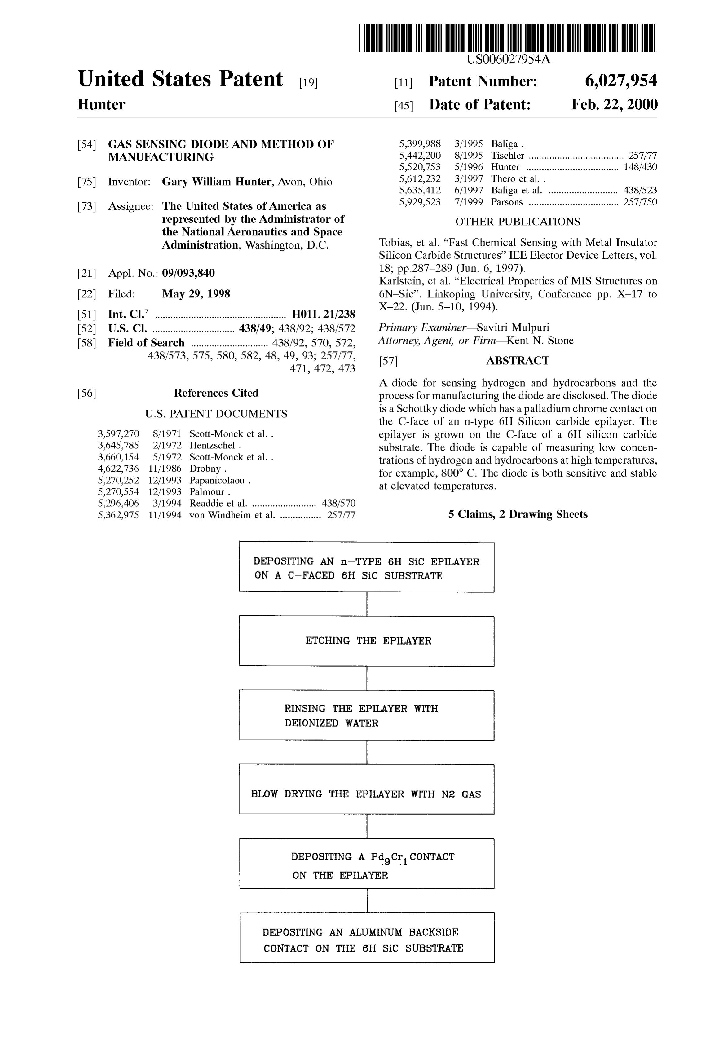
United States Patent (19) 11 Patent Number: 6,027,954 Hunter (45) Date of Patent: Feb. 22, 2000 54). GAS SENSING DIODE AND METHOD OF 5,399,988 3/1995 Baliga. MANUFACTURING 5,442,200 8/1995 Tischler ..................................... 257/77 5,520,753 5/1996 Hunter .................................... 148/430 75 Inventor: Gary William Hunter, Avon, Ohio 5,612.232 3/1997 Thero et al. 5,635,412 6/1997 Baliga et al. ........................... 438/523 73 Assignee: The United States of America as 5,929,523 7/1999 Parsons ................................... 257/750 represented by the Administrator of OTHER PUBLICATIONS the National Aeronautics and Space
Administration, Washington, D.C. Tobias, et al. “Fast Chemical Sensing with Metal Insulator Silicon Carbide Structures' IEEElector Device Letters, vol.
21 Appl. No.: 09/093,840 18; pp.287–289 (Jun. 6, 1997). Karlstein, et al. “Electrical Properties of MIS Structures on 22 Filed: May 29, 1998 6N-Sic'. Linkoping University, Conference pp. X-17 to (51) Int. Cl." ................................................... H01L 21/238 X-22. (Jun. 5–10, 1994). 52 U.S. Cl. ............ . . 438/49; 438/92; 438/572 Primary Examiner Savitri Mulpuri 58 Field of Search .............................. 438/92, 570, 572, Attorney, Agent, or Firm-Kent N. Stone 438/573, 575, 580, 582, 48, 49, 93; 257/77, 57 ABSTRACT
A diode for Sensing hydrogen and hydrocarbons and the 56) References Cited process for manufacturing the diode are disclosed. The diode
the C-face of an n-type 6H Silicon carbide epilayer. The 3,597.270 8/1971 Scott-Monck et al.. epilayer is grown on the C-face of a 6H Silicon carbide 3,645,785 2/1972 Hentzschel. Substrate. The diode is capable of measuring low concen 3,660,154 5/1972 Scott-Monck et al.. trations of hydrogen and hydrocarbons at high temperatures, 4,622,736 11/1986 Drobny. for example, 800° C. The diode is both sensitive and stable 5,270,252 12/1993 Papanicolaou. at elevated temperatures.
5,296,406 3/1994 Readdie et al. ......................... 438/570 5,362.975 11/1994 von Windheim et al. ................ 257/77 5 Claims, 2 Drawing Sheets
DEPOSITING AN n-TYPE 6H SiC EPILAYER
ON A C-FACED 6H SiC SUBSTRATE
ETCHING THE EPIAYER
RINSING THE EPAYER WITH
DEONIZED WATER
BLOW DRYING THE EPLAYER WITH N2 GAS
DEPOSITING A PdCrCONTACT
ON THE EPLAYER
DEPOSITING AN ALUMNUM BACKSIDE
CONTACT ON THE 6H SiC SUBSTRATE
Page 2
Drawing sheet — no readable text.
Page 3
DEPOSITING AN n-TYPE 6H SiC EPLAYER ON A C-FACED 6H SiC SUBSTRATE
ETCHING THE EPILAYER
RINSING THE EPILAYER WITH
DEIONIZED WATER
BLOW DRYING THE EPLAYER WITH N2 GAS
DEPOSITING A Pd 91
C CONTACT
ON THE EPILAYER
DEPOSITING AN ALUMINUM BACKSIDE
CONTACT ON THE 6H SiC SUBSTRATE
Page 4
GAS SENSING DODE AND METHOD OF It is an object of the invention to provide a sensor which MANUFACTURING is stable and sensitive at high temperatures of 425 C. and above.
ORIGIN OF THE INVENTION It is a further object of the present invention to provide a The invention described herein was made by an employee palladium chrome contact on an alpha 6H Silicon carbide Substrate with a metal backside contact.
of the United States Government and may be manufactured and used by or for the Government for Government pur It is an object of the present invention to provide a gas poses without the payment of any royalties thereon or Sensor using an alloy on the C-face of a Silicon carbide therefor. epilayer on a Silicon carbide Substrate. It is an object of the present invention to provide a Sensor
FIELD OF THE INVENTION which is stable and Sensitive following exposure to high The instant invention is a Schottky diode. Its principal use temperatures for long periods of time. is the measurement of hydrogen and hydrocarbons occurring It is an object to provide a Schottky diode employing at low concentrations and high temperatures. 15 Silicon carbide as the Semiconductor to detect hydrogen and hydrocarbons at low concentrations.
BACKGROUND OF THE INVENTION It is an object to provide a hydrogen and/or hydrocarbon U.S. Pat. No. 5,270,252 to Papanicolaou is a Schottky prolongedSensor which can be used at elevated temperatures for periods of time for use in catalytic combustion diode on beta Silicone carbide. The metals taught in the control Systems or other applications which depend on the Papanicolaou disclosure are platinum, tungsten, titanium presence of hydrogen or hydrocarbons.
tungsten, gold and aluminum. The Schottky diode of the
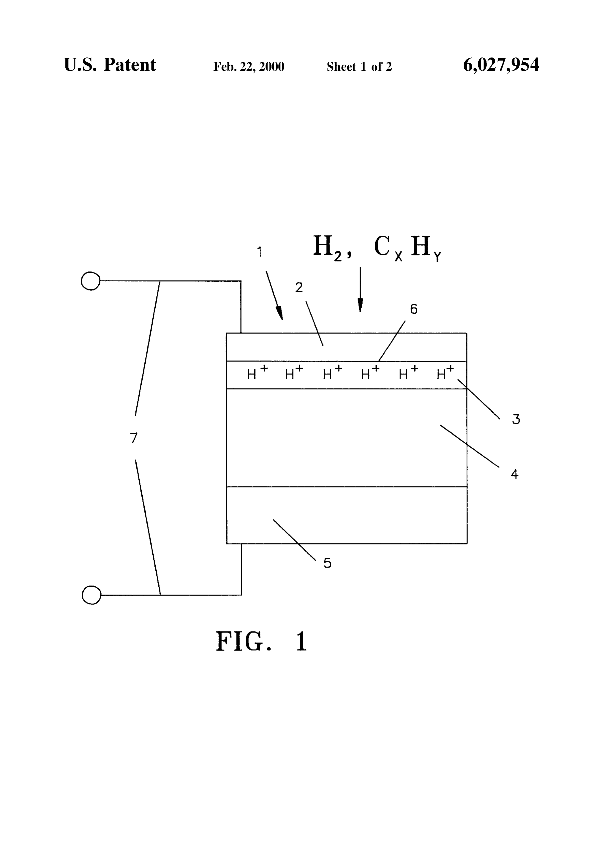
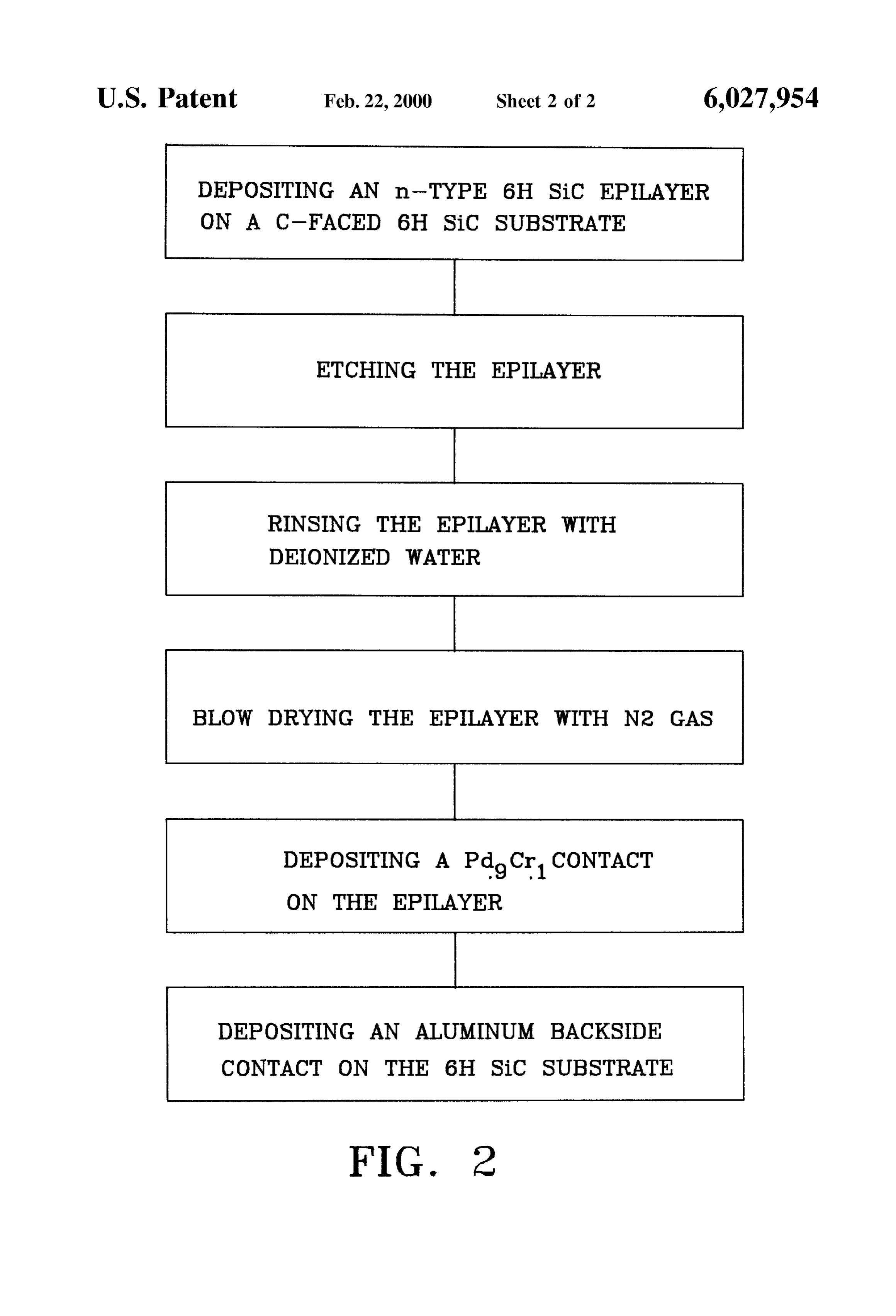
Papanicolaou disclosure is used for high temperature Semi BRIEF DESCRIPTION OF THE DRAWINGS conductor applications and, in particular, it is used as a rectifying diode. Drawing FIG. 1 illustrates the PdCro contact on the 25 C-face of an O. Silicon Carbide epilayer on the C-face of the
U.S. Pat. No. 5,612,232 to Thero, et al. is a Schottky diode C. Silicon Carbide Substrate. Abackside metal contact is also for use in high temperature applications but it cannot be used shown.
as a gas Sensor. Thero, et al. teaches the use of a Silicon Drawing FIG. 2 schematically illustrates the process for carbide Semiconductor with nickel and tungsten as metals. manufacturing the Schottky diode. U.S. Pat. No. 4,622,736 to Drobny discloses Schottky diodes for use in connection with a Silicon Semiconductor. DETAILED DESCRIPTION OF THE Tungsten, titanium-tungsten, and Vanadium are the metals INVENTION used in the invention. The Drobny Schottky diode is not a A Schottky diode is formed by the junction of a metal and gas Sensor. a semiconductor. Other diodes are formed by the junction of The development of a Schottky diode structure has been 35 a p-type and an n-type Semiconductor.
reported by the researchers at Linkoping University. The FIG. 1 is a schematic representation of the structure of the structure of the Linkoping sensor is Pt on TaSix on SiO2 on invention. FIG. 2 is a Schematic of the process used SiC. The Pt/TaSix/SiO2 thicknesses are 100 nm/10 nm/5 nm.
respectively. The Sensor responses are stable and fast but (described above) to manufacture the instant invention. The they are not highly Sensitive. 40 advantage of the Schottky diode 1 of the present invention is that a large Signal difference is obtained in response to a
SUMMARY OF THE INVENTION corresponding Small concentration of hydrogen or hydro carbons in high temperature applications. The Schottky
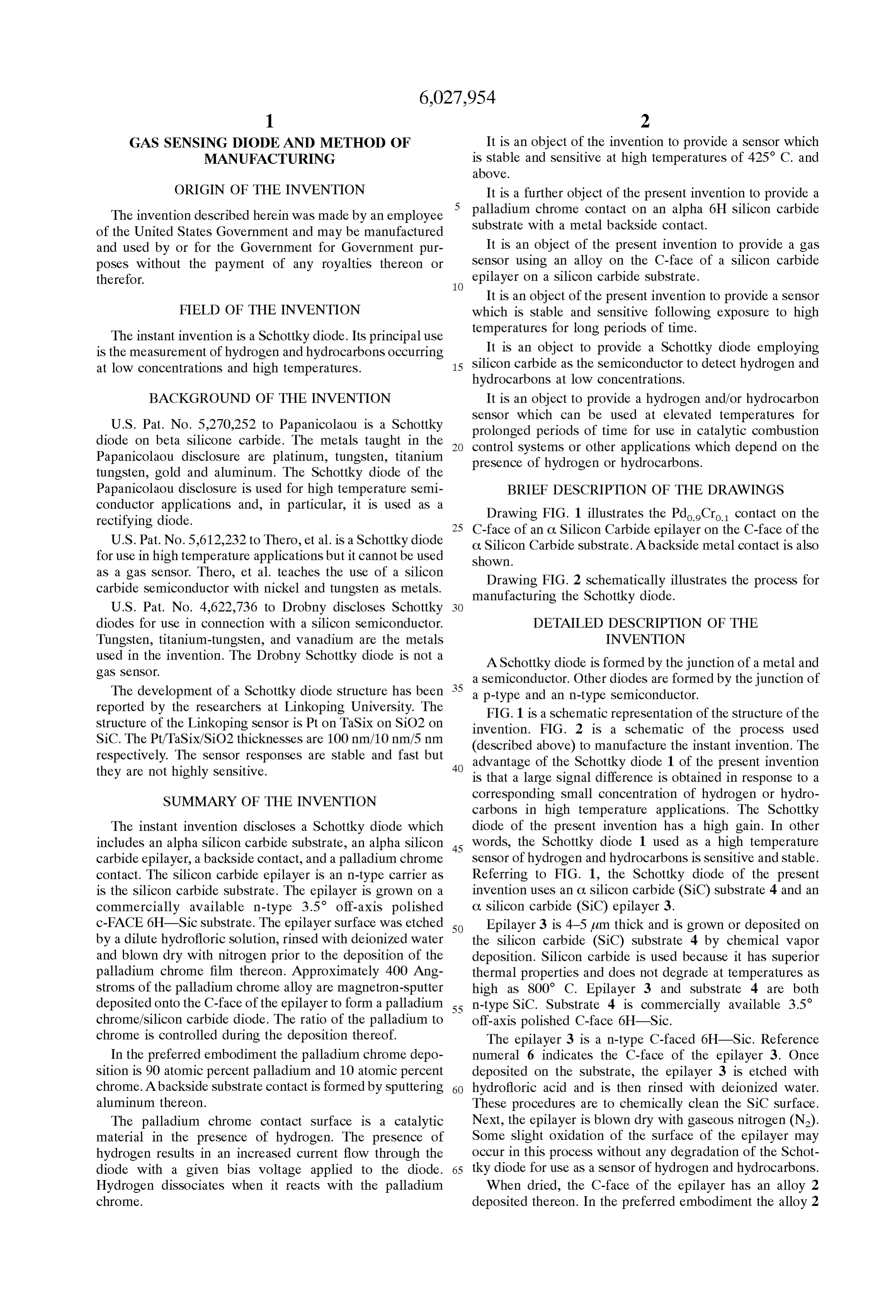
The instant invention discloses a Schottky diode which diode of the present invention has a high gain. In other includes an alpha Silicon carbide Substrate, an alpha Silicon 45 words, the Schottky diode 1 used as a high temperature carbide epilayer, a backside contact, and a palladium chrome Sensor of hydrogen and hydrocarbons is Sensitive and Stable. contact. The Silicon carbide epilayer is an n-type carrier as Referring to FIG. 1, the Schottky diode of the present is the Silicon carbide Substrate. The epilayer is grown on a invention uses an O. Silicon carbide (SiC) Substrate 4 and an commercially available n-type 3.5 off-axis polished C. silicon carbide (SiC) epilayer 3.
c-FACE 6H-Sic substrate. The epilayer surface was etched 50 Epilayer 3 is 4-5 um thick and is grown or deposited on by a dilute hydrofloric solution, rinsed with deionized water the silicon carbide (SiC) substrate 4 by chemical vapor and blown dry with nitrogen prior to the deposition of the deposition. Silicon carbide is used because it has Superior palladium chrome film thereon. Approximately 400 Ang thermal properties and does not degrade at temperatures as Stroms of the palladium chrome alloy are magnetron-Sputter high as 800° C. Epilayer 3 and substrate 4 are both deposited onto the C-face of the epilayer to form a palladium 55 n-type SiC. Substrate 4 is commercially available 3.5 chrome/silicon carbide diode. The ratio of the palladium to off-axis polished C-face 6H-Sic.
chrome is controlled during the deposition thereof. The epilayer 3 is a n-type C-faced 6H-Sic. Reference In the preferred embodiment the palladium chrome depo numeral 6 indicates the C-face of the epilayer 3. Once Sition is 90 atomic percent palladium and 10 atomic percent deposited on the substrate, the epilayer 3 is etched with chrome. Abackside Substrate contact is formed by Sputtering 60 hydrofloric acid and is then rinsed with deionized water. aluminum thereon. These procedures are to chemically clean the SiC Surface. The palladium chrome contact Surface is a catalytic Next, the epilayer is blown dry with gaseous nitrogen (N). material in the presence of hydrogen. The presence of Some slight oxidation of the Surface of the epilayer may hydrogen results in an increased current flow through the occur in this process without any degradation of the Schot diode with a given bias Voltage applied to the diode. 65 tky diode for use as a Sensor of hydrogen and hydrocarbons. Hydrogen dissociates when it reacts with the palladium When dried, the C-face of the epilayer has an alloy 2 chrome. deposited thereon. In the preferred embodiment the alloy 2
Page 5
is palladium chrome (PdCr). The palladium chrome alloy is What is claimed is:
deposited onto the C-face of the epilayer using magnetron 1. A process for manufacturing a Schottky diode having Sputtering. Approximately 400 Angstrums of palladium an n-type polished 6H Silicon carbide Substrate, an n-type chrome are used in the preferred embodiment. However, 6Hsilicon carbide epilayer, a 400 Angstrom thick palladium 300-1000 Angstroms of an alloy such as palladium chrome chrome contact and a backside contact, comprising the Steps may be used. Other forms of physical deposition can be used of:
as well Such as evaporation. Chemical vapor deposition may depositing an n-type C-faced 6H Silicon carbide epilayer also be used. The ratio of palladium is 90 atomic percent to on a polished C-face of a 6H silicon carbide substrate; 10 atomic percent chrome. This ratio may vary from about etching Said epilayer with an acid Solution; 70 to 95 atomic percent palladium to 5 to 30 atomic percent rinsing Said epilayer;
chrome. Palladium dissociates hydrogen. A backside metal drying Said epilayer;
lic contact 5 is affixed to the SiC substrate 4 by magnetron depositing palladium and chrome on Said epilayer; and, Sputtering. In the preferred embodiment the contact 5 is aluminum. depositing a metallic backside contact on Said 6H Silicon carbide Substrate.
The thermal stability of the Schottky diode of the pre 15 2. A process as claimed in claim 1 wherein Said Step of ferred embodiment, to wit, PdCro/6H-Sic, is improved depositing palladium and chrome comprises depositing 90 compared to a Pd/SiC diode. Further, the response of a atomic percent palladium and 10 atomic percent chrome. Pdoo Cro/6H-Sic diode to hydrogen is stable after long 3. A process as claimed in claim 2 wherein Said Step of heating periods. depositing a metallic backside contact comprises depositing Reference numeral 7 indicates the Sensor electrical con an aluminum backside contact.
nections. A bias Voltage is applied to the Schottky diode 1 4. A process as claimed in claim 3 wherein Said Step of (i.e., the Sensor) in operation and the presence of hydrogen depositing palladium and chrome comprises magnetron or hydrocarbons causes a change in the current measured in Sputtering Said palladium and chrome.
the circuit. 5. A process as claimed in claim 4 wherein Said Step of
The foregoing description of the invention has been Set depositing an aluminum backside contact comprises mag forth by way of example only and in no way limits the Scope netron Sputtering Said aluminum backside contact. of the invention. The scope of the invention is set forth in the attached claims. k k k k k
Provenance
- Collection
- Cited prior art
- Original PDF
- patentimages.storage.googleapis.com →
- Filed
- 1998-05-29
- Pages
- 5
- Method
- pdftotext (the PDF's own text layer) + pdftoppm 300dpi page scans
- Source
- Google Patents bibliographic record
- Granted
- 2000-02-22
- Inventors
- Gary William Hunter; National Aeronautics and Space Administration NASA
- Transcribed from
- patentimages.storage.googleapis.com →