patent · US6255133
Electro optical devices with reduced filter thinning on the edge pixel photosites and method of producing same
3 July 2001
Page 1 — bibliographic record
(12) United States Patent (10) Patent No.: US 6,255,133 B1 Ormond et al. (45) Date of Patent: *Jul. 3, 2001
(54) ELECTRO OPTICAL DEVICES WITH 4,814,296 3/1989 Jedlicka et al. ...................... 437/226 REDUCED FILTER THINNING ON THE 5,153,421 10/1992 Tandon et al. .................... 250/208.1 EDGE PIXEL PHOTOSITES AND METHOD 5,340.619 8/1994 Chen et al. .......................... 424/498 OF PRODUCING SAME 5,473,513 12/1995 Quinn ................................... 361/760 5,521,125 5/1996 Ormond et al. ..................... 437/227 (75) Inventors: Brian T. Ormond, Webster; Josef E. 5.530,278 6/1996 Jedlicka et al. ...................... 257/233 Jedlicka, Rochester; Thomas 5,604,362 2/1997 Jedlicka et al. ...................... 257/233 Grimsley, Fairport; Paul A. Hosier, 5,848,331 12/1998 Fromm ........ ... 399/122 Rochester, all of NY (US) 6,111.247 O
(73) Assignee: Xerox Corporation, Stamford, CT
(US) Primary Examiner Savitri Mulpuri (*) Notice: Subject to any disclaimer, the term of this (74) Attorney, Agent, or Firm-P. Daebeler patent is extended or adjusted under 35
U.S.C. 154(b) by 0 days. (57) ABSTRACT
This patent is Subject to a terminal dis The present invention relates to electro optical devices with claimer. a reduced filter thinning on the edge pixels and a method for reducing the thinning of filter layers on the pixels closest to (21) Appl. No.: 09/641,292 the edge of an electro optical device Such as a photoSensitive chip, as would be used, for example, in a full-color digital (22) Filed: Aug. 18, 2000 copier or Scanner. A Semiconductor wafer includes a main Related U.S. Application Data Surface defining a plurality of chip areas and tab regions Separated by grooves, wherein the chip areas include inner (62) Division of application No. 09/196,462, filed on Nov. 19, photoSites, outer photoSites and bonding pads. A plurality of 1998, now Pat. No. 6,201,293. dams are deposited over the main Surface in the tab regions, (51) Int. Cl." ............................................... H01L 21/302 and a clear layer is deposited over the main Surface exclusive (52) U.S. Cl. ................................. 438/57; 438/81; 438/70; of the bonding pads. Alternatively, a clear layer is deposited 438/75; 438/462 over the main Surface exclusive of the bonding pads, and a (58) Field of Search .................................. 438/57, 60, 65, plurality of tabs is then deposited in the tab regions on the 438/68, 70, 75, 73, 80, 81, 460, 462, 795; main Surface. A first primary color filter layer is deposited 257/225, 431, 432, 667, 233 over at least first inner photoSite and first outer photoSite, (56) References Cited and the first primary color filter layer transmits a primary color.
4,315,978 2/1982 Hartman ................................... 430/4 4 Claims, 6 Drawing Sheets
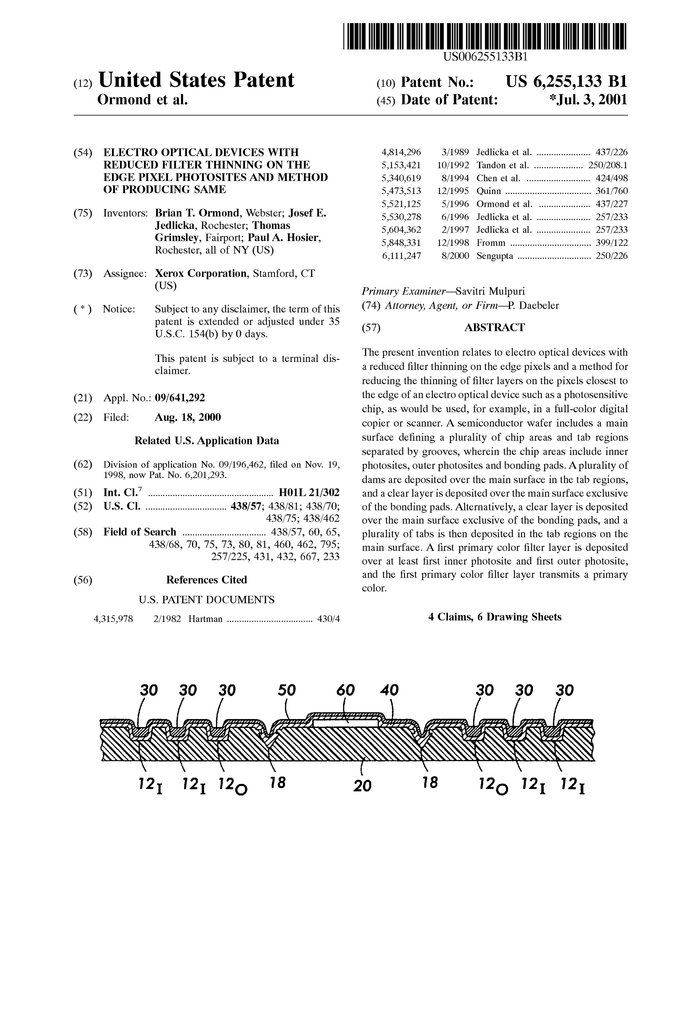
30 30 30 50 6O 40 3O 3O 3O
az722azz,Aa w a Lazzazz a
12I 721 12o 18 2O 18 12o 12 12
Page 2
Drawing sheet — no readable text.
Page 3
Drawing sheet — no readable text.
Page 4
Drawing sheet — no readable text.
Page 5
Drawing sheet — no readable text.
Page 6
Drawing sheet — no readable text.
Page 7
Drawing sheet — no readable text.
Page 8
ELECTRO OPTICAL DEVICES WITH one primary color. Typically, this arrangement can be REDUCED FILTER THINNING ON THE achieved by providing multiple linear arrays of photosensors EDGE PIXEL PHOTOSITES AND METHOD which are physically identical except for a translucent OF PRODUCING SAME primary-color overlay over the photosensitive areas, or “photosites,” for that linear array. In other words, the linear
This application is a divisional of application Ser. No. array which is Supposed to be sensitive to red light only will 09/196,462, filed Nov. 19, 1998 now U.S. Pat. No. 6,201, have a translucent red layer placed on the photoSites thereof, 293. and Such would be the case for a blue-Sensitive array and a Attention is directed to copending application Attorney green-Sensitive array. AS the chip is exposed to an original Docket No. D/98036, U.S. patent application Ser. No. full-color image, only those portions of the image which 09/196,441, filed Nov. 19, 1998, entitled, “ELECTRO correspond to particular primary colors will reach those OPTICAL DEVICES WITH REDUCED FILTER THIN photosensors assigned to the primary color. NING ON THE EDGE PIXEL PHOTSITES AND The most common Substances for providing these trans METHOD FOR PRODUCING SAME'. The disclosure of lucent filter layers over the photoSites is polyimide or this copending application is hereby incorporated by refer 15 acrylic. For example, polyimide is typically applied in liquid ence in its entirety. form to a batch of photosensor chips while the chips are still
FIELD OF THE INVENTION
in undiced, wafer form. After the polyimide liquid is applied to the wafer, the wafer is centrifuged to provide an even
The present invention relates to electro optical devices layer of a particular polyimide. In order to obtain the with a reduced filter thinning on the edge or outer pixel polyimide having the desired primary-color-filtering photoSites and a method for reducing the thinning of filter properties, it is well known to dope the polyimide with either layerS on the pixel photoSites closest to the edge of an electro a pigment or dye of the desired color, and these dopants are optical device Such as a photosensitive chip, as would be readily commercially available. When it is desired to place used, for example, in a full-color digital copier or Scanner. 25 different kinds of color filters on a single chip, a typical technique is to first apply an even layer of polyimide over
BACKGROUND OF THE INVENTION the entire main Surface of the chip (while the chip is still part Image Sensors for Scanning document images, Such as of the wafer) and then remove the unnecessary parts of the charge coupled devices (CCDs), typically have a row or filter by photo-etching or another well known technique. linear array of photoSites together with Suitable Supporting Typically, all of the filter layer placed over the chip is circuitry integrated onto a Semiconductor chip. Usually, a removed except for those areas over the desired Set of Sensor is used to Scan line by line acroSS the width of a photoSites. Acrylic is applied to the wafer in a similar
document with the document being moved or Stepped lengthwise in Synchronism therewith. A typical architecture SUMMARY OF THE INVENTION for Such a Sensor array is given, for example, in U.S. Pat. No. 35 According to a first embodiment of the present invention, 5,153,421. a Semiconductor wafer includes a main Surface defining a In a full-page-width image Scanner, there is provided a plurality of chip areas and tab regions Separated by grooves, linear array of photosensors which extends the full width of wherein the chip areas include inner photoSites, Outer pho an original document, Such as eleven inches. When the toSites and bonding pads. A plurality of dams are deposited original document moves past the linear array, each of the 40 over the main Surface in the tab regions, and a clear layer photoSensors converts reflected light from the original image deposited over the main Surface and dams exclusive of the into electrical Signals. The motion of the original image bonding pads. A first primary color filter layer is deposited perpendicular to the linear array causes a Sequence of Signals over at least first inner photoSite and first outer photoSite, to be output from each photosensor, which can be converted wherein the first primary color filter layer transmits a into digital data. 45 primary color. A Second primary color filter layer is depos A currently-preferred design for creating Such a long ited over at least a Second inner photoSite and a Second outer linear array of photoSensors is to provide a set of relatively photoSite, wherein the Second primary color filter layer Small Semiconductor chips, each Semiconductor chip defin transmits a Second primary color. A third primary color filter ing thereon a linear array of photoSensors along with ancil layer is deposited over at least a third inner photoSite and a lary circuit devices. These chips are assembled end-to-end to 50 third outer photosite, wherein the third primary color filter form a single linear array of photoSensors as disclosed in layer transmits a third primary color. The dams consist of U.S. Pat. No. 5,473,513. However, a single chip having a aluminum, polyimide or acrylic, and the filter layerS and the linear array may also be used for Sensing images and clear layer consist of polyimide or acrylic.
converting those images into electrical Signals to be output According to a Second embodiment, a Semiconductor from each photosensor, which can be converted into a digital 55 wafer includes a main Surface defining a plurality of chip Signal. These chips can also be assembled end to end to form areas and tab regions Separated by grooves, wherein the chip a full width array comprising a multiple parallel linear arrayS areas include inner photoSites, Outer photoSites and bonding of photoSites. pads, and wherein a clear layer is deposited on the main With the gradual introduction of color-capable products Surface exclusive of the bonding pads. A plurality of dams into the office equipment market, it has become desirable to 60 are placed on the clear layer on the main Surface in the tab provide Scanning Systems which are capable of converting regions, and a first primary color filter layer is deposited light from full-color images into Separate trains of image over at least first inner photoSite and first outer photoSite. Signals, each train representing one primary color. In order The first primary color filter layer transmits a primary color. to obtain the Separate Signals relating to color Separations in A Second primary color filter layer is deposited over at least a full-color image, one technique is to provide on a Semi 65 a Second inner photoSite and a Second outer photoSite, conductor chip multiple parallel linear arrays of wherein the Second primary color filter layer transmits a photoSensors, each of the parallel arrays being Sensitive to Second primary color. A third primary color filter layer is
Page 9
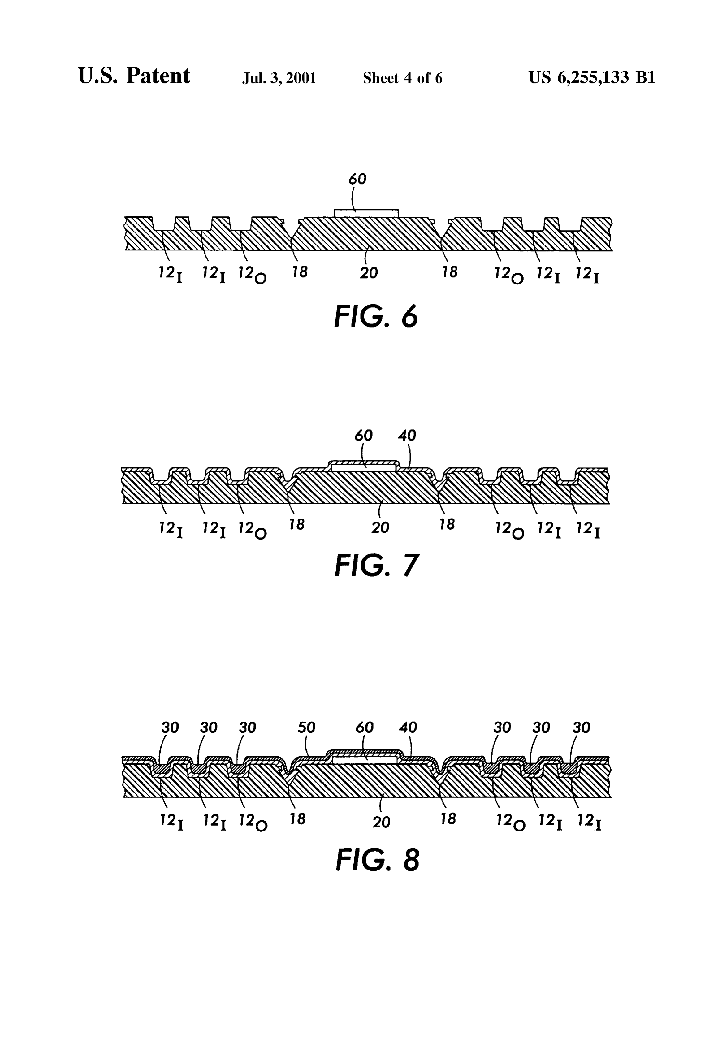
deposited over at least a third inner photoSite and a third FIG. 8 shows a filter layer deposited on the section of the outer photoSite, wherein the third primary color filter layer semiconductor wafer shown in FIG. 6 in accordance with the transmits a third primary color. The dams consist of first embodiment of the present invention;
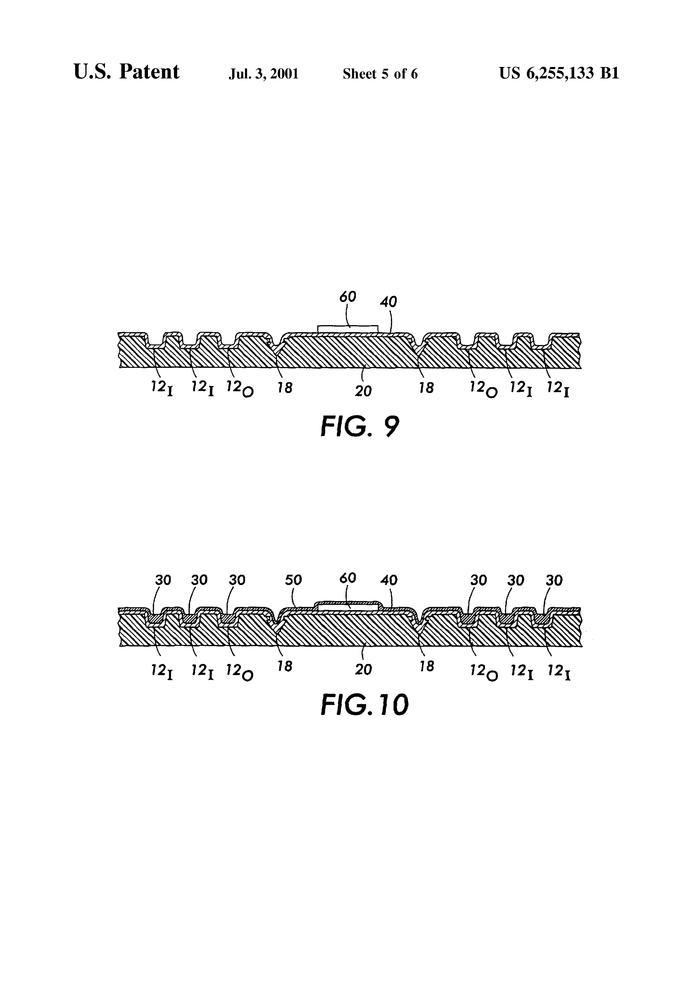
aluminum, polyimide or acrylic, and the filter layerS and the FIG. 9 shows a clear layer deposited on a section of the clear layer consist of polyimide or acrylic. Semiconductor wafer and a dam formed in a tab region on A method for fabricating the photosensitive chips of the the clear layer according to a Second embodiment of the first embodiment comprises providing a Semiconductor present invention;
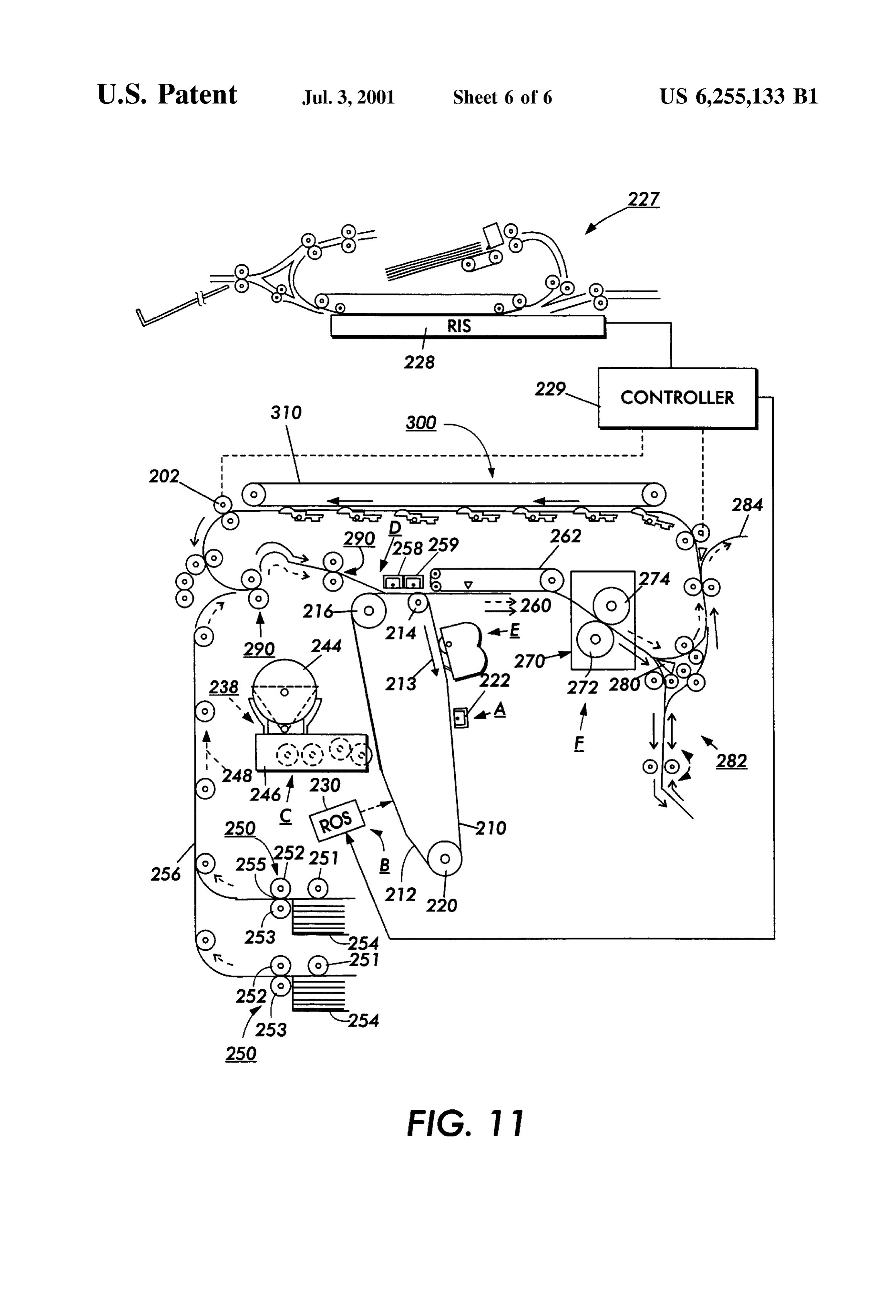
wafer having a main Surface defining chip areas Separated by FIG. 10 shows a filter layer deposited on the section of the V-grooves, the chip areas defining bonding pads and three semiconductor wafer shown in FIG. 9 according to the rows of photoSites, wherein the photoSites include inner Second embodiment of the present invention; and photoSites, outer photoSites and bonding pads, depositing FIG. 11 is a partial schematic elevational view of an dams in tab regions on the Semiconductor wafer; hard example of a digital copier, which employs the photosensi baking the Semiconductor wafer, depositing a clear layer on tive chips of the present invention.
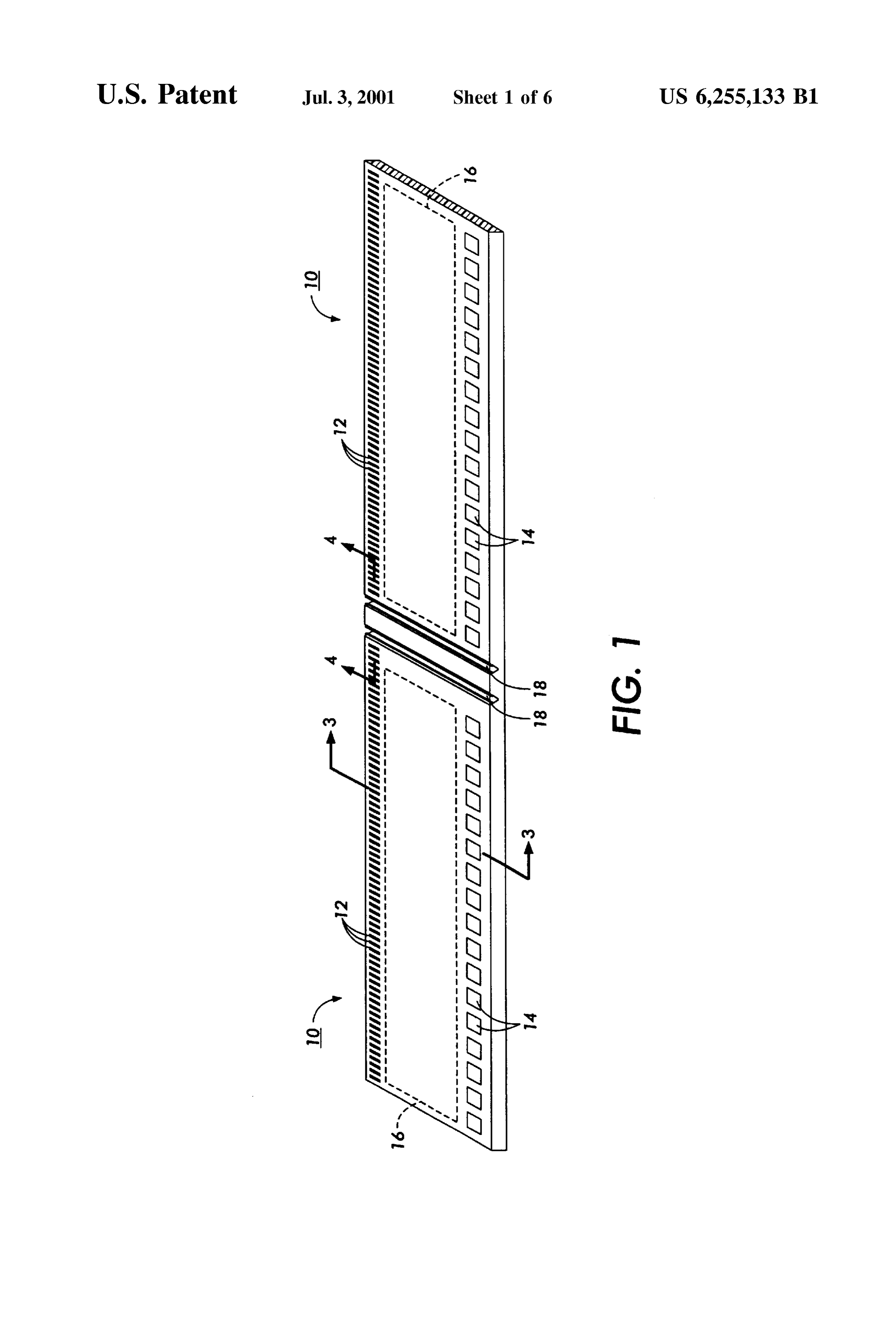
the Semiconductor wafer; Soft baking the Semiconductor wafer, exposing Selective areas of a Semiconductor wafer; 15 DETAILED DESCRIPTION OF THE PRESENT etching the clear layer covering the bonding pads from the INVENTION Semiconductor wafer; hard baking the Semiconductor wafer; FIG. 1 is a perspective view showing two photosensitive and depositing a first primary color filter layer over at least chips 10 relevant to the claimed invention. The chips 10 are first inner photoSite and first outer photoSite, the first primary generally made of a Semiconductor Substrate, as is known in color filter transmitting a primary color. The method for the art, in which circuitry and other elements are formed, fabricating the Semiconductor chip further includes dicing Such as by photolithographic etching. A few of the most the Semiconductor wafer to produce the Semiconductor chip relevant Structures are a linear array of pixel photoSites 12, for Single chip applications or for assembly on a Substrate to each of which forms the photosensitive surface of photo provide a full width array. Sensor circuitry within each chip 10, and a set of bonding A method for fabricating the photosensitive chips of the 25 pads 14. The pixel photoSites 12 are typically arranged in a Second embodiment comprising providing a Semiconductor linear array along one main dimension of each chip 10, with wafer having a main Surface defining chip areas Separated by each pixel photoSite 12 along the array corresponding to one V-grooves, the chip areas defining bonding pads and three pixel in the image Signal. AS will be described in detail rows of photoSites, wherein the photoSites include inner below, the pixel photosite 12 includes photosites 12B, 12G photoSites, outer photoSites and bonding pads, depositing and 12R for Sensing the three primary colors (blue, green first clear layer on the Semiconductor wafer, Soft baking the and red) corresponding to the pixel.
Semiconductor wafer; exposing Selective areas of a Semi The bonding pads 14 are distinct Surfaces on the main conductor wafer, etching the first clear layer covering the Surface of the chips 10, and are intended to accept wire bonding pads from the Semiconductor wafer; hard baking bonds attached thereto. The bonding pads 14 thus serve as the Semiconductor wafer, depositing dams in tab regions on 35 the electronic interface between the chips 10 and any the Semiconductor wafer; hard baking the Semiconductor external circuitry. The circuitry for obtaining Signals related wafer; and depositing a first primary color filter layer over to light directed to the pixel photoSites 12, and unloading at least first inner photoSite and first Outer photoSite, the first image data from the chips 10 is generally indicated as 16, primary color filter layer transmitting a primary color. The and is generally deposited between the linear array of pixel Semiconductor wafer is diced to provide the Semiconductor 40 photoSites 12 and a Substantially linear array of bonding chip for Single applications or for assembly on a Substrate to pads 14.
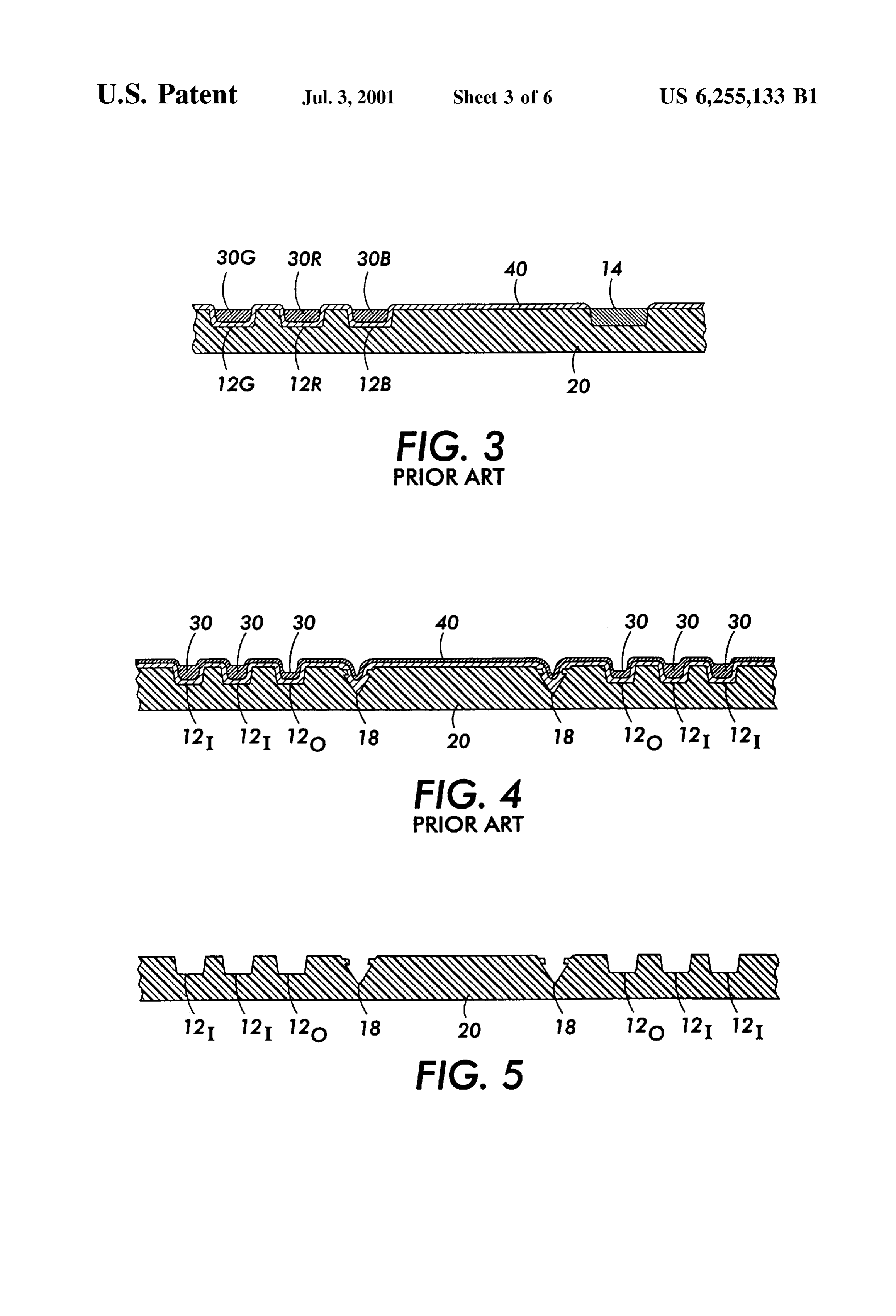
provide a full width array. Chips 10 are typically formed in batches on semiconduc BRIEF DESCRIPTION OF THE DRAWINGS tor wafers, which are Subsequently cleaved, or "diced, to FIG. 1 is a perspective view showing two chips relevant 45 create individual chips. Typically, the Semiconductor wafers are made of Silicon. AS is known in the art, to the present invention; photolithographically-etched V-grooves 18 define precisely FIG. 2 is a perspective view showing a Semiconductor the intended boundaries of a particular chip 10 for dicing. water relevant to the present invention; Thus, all of the pixel photosites 12, bonding pads 14 and FIG. 3 is a cross-sectional view through line 3-3 in the circuitry 16 for relatively large number of chips 10 are direction of the arrows in FIG. 1, showing polyamide or 50 etched simultaneously onto a Single Semiconductor wafer 20 acrylic layerS deposited on a Section of the Semiconductor as shown in FIG. 2. The region between the V-grooves 18 is wafer in accordance with the prior art; called the tab region. The pixel photosite 12 adjacent to each FIG. 4 is a partial cross-sectional view through line 4-4 V-groove is referred to as an outer pixel photoSite 12. Each in the direction of the arrows in FIG. 1, showing polyimide outer pixel photoSite 12, consists of three Outer photoSites or acrylic layerS deposited on a Section of the Semiconductor 55 12B, 12G, and 12R. The other pixel photosites 12 are wafer in accordance with the prior art; referred to as inner pixel photoSites 12, and each inner pixel FIG. 5 is a partial cross-sectional view through line 4-4 photosite 12 consists of three inner photosites 12B, 12G, in the direction of the arrows in FIG. 1, showing a section and 12R.
of the Semiconductor wafer before a clear layer is deposited FIG. 2 shows a typical semiconductor wafer 20, in in accordance with the embodiments of the present inven 60 isolation, wherein a relatively large number of chipS 10 are tion; created in the wafer 20 prior to dicing thereof. Each indi FIG. 6 shows a section of the semiconductor wafer of vidual chip 10 has a distinct chip area within the main FIG. 5 on which a dam is deposited in a tab region in surface of the wafer 20. The phrase “chip area” refers to a accordance with a first embodiment of the present invention; defined area within the main Surface of the wafer 20 which FIG. 7 shows a clear layer deposited on the section of the 65 is intended to comprise a discrete chip 10 after the dicing semiconductor wafer shown in FIG. 6 in accordance with the step, when individual chips 10 are separated from the rest of first embodiment; the wafer 20.
Page 10
S 6
FIG. 3 is a cross sectional view through line 3-3 in the If only one filter layer 30 was to be deposited on semi direction of the arrows of FIG. 1. On the main Surface of conductor wafer 20, then the semiconductor wafer 20 would chip 10 there is provided an inner pixel photosite 12, with be Soft baked. Then, certain areas of the Semiconductor three separate photosites 12B, 12G and 12R, each sensitive wafer 20 would be selectively exposed to ultraviolet light to one primary color. As shown in the FIG. 3, within each using a mask and the filter layer 30 would be etched out of inner pixel photosite 12, is deposited a photosite 12G, the semiconductor wafer 20 except for the pixel photosites Sensitive to greenlight, a photoSite 12R Sensitive to red light, 12. The semiconductor wafer 20 would then be hard baked and a photosite 12B, sensitive to blue light. The three and diced to provide chips 10. photosites 12B, 12G and 12R are on the whole identical as However, two additional filter layers 30 are preferably circuit elements except that the Surface of each photoSite added to semiconductor wafer 20. Therefore, after the first 12B, 12G and 12R is superimposed thereon by a distinct filter layer 30 is deposited on the semiconductor wafer 20, primary-color filter 30. The blue filter layer, the green filter the semiconductor wafer 20 is Soft baked. Certain areas of layer and the red filter layer are indicated by reference the Semiconductor wafer 20 are Selected for exposure to numerals 30B, 30G, and 30R. ultraviolet light using a mask. Preferably, the filter layer 30 AS is known in the art, Such filters preferably comprise a 15 isrowetched out of the semiconductor wafer 20 except for one polyimide or acrylic which has been doped with a partialof cross photoSites in each chip area, which is shown by the section of chips 10 in FIG. 8. The two other commercially-available dye or pigment blended to yield a rows of photoSites in each chip area have Substantially the primary color filter. AS is further known in the art, it is Same configuration as shown in the partial croSS Section of common to provide filters such as 30B, 30G and 30R, by chips 10 in FIG. 7. A second filter layer 30 is deposited on first placing a polyimide or acrylic in liquid form over the the semiconductor wafer 20, and these two rows now have entire main Surface of the chip 10, and then removing the substantially the same configuration as shown in FIG.8. The polyimide or acrylic by photolithography in all areas of the semiconductor wafer 20 is then soft baked, selectively chip 10 except where the filter area is desired. To ensure a exposed to ultraViolet light, Selectively etched and hard uniform coating of these materials, the Semiconductor wafer baked So that two rows of photoSites in each chip area each 20 is partially planarized by using clear layer 40, which is 25 have a different filter layer 30. The two rows having filter preferably a clear polyimide or clear acrylic layer. This clear layerS 30 in each chip area have Substantially the same layer 40 acts to Smoothen the topography of the Semicon configuration as shown by the partial croSS Section in FIG. ductor wafer 20 and partially fill the V-grooves 18 as shown 8. The last row of photosites, which does not have a filter in FIG. 4. Since the clear layer 40 only partially planarizes layer 30, has Substantially the same configuration as shown the semiconductor wafer 20, the V-grooves 18 still allow in the partial cross section in FIG. 7.
Some of the filter material to be channeled away from the A third filter layer 30 is deposited on the semiconductor outer pixel photosites 12, causing thinning of the filter wafer 20. The semiconductor wafer 20 is then Soft baked, material over the outer pixel photoSites 12, as shown in FIG. Selectively exposed to ultraviolet light, Selectively etched 4. The outer pixel photosites 12 on the semiconductor wafer and hard baked so that three rows of photosites now have 20 have substantially thinner filter layers 30 than the inner 35 substantially the same configuration as shown in FIG. 8. photoSite pixels 12 due to the chip topography of the However, each filter layer 30 preferably has a different filter semiconductor wafer 20 as explained above. The two material. Preferably, the three filter layers 30 are red, green embodiments of the present invention enhance the image and blue.
Sensing capability of the photosensitive chips 10 by increas In the Second embodiment of the present invention, a clear ing the thickness of the filter layers of the Outer pixel 40 layer 40 is deposited on the semiconductor wafer 20. The photoSites 12. coated semiconductor wafer 20 is soft baked (partially FIG. 5 is a cross-sectional view through line 4-4 in the baked), and certain areas of the Semiconductor wafer 20 are direction of the arrows in FIG. 1, showing a section of the Selected for exposure to ultraViolet light using a mask. The semiconductor wafer 20 before the acrylic or polyimide clear layer 40 is etched out of the bonding pads 14. An layers are deposited in accordance with the first embodiment 45 etched out bonding pad is shown in FIG. 3. Then, at least one of the present invention. Then, an aluminum, polyimide or aluminum, polyimide or acrylic dam 60 is deposited in the acrylic dam 60 is deposited on at least one tab region as tab region and on the clear layer 40 as shown in FIG. 9. shown in FIG. 6. Preferably, a dam 60 is deposited in each Preferably, a dam 60 is deposited in each tab region between tab region between the chips 10 on the semiconductor wafer the chips 10 on the clear layer 40 of the semiconductor wafer 20. A clear layer 40, which is preferably polyimide or 50 20. According to the Second embodiment of the present acrylic, is deposited on the Semiconductor wafer 20 includ invention, the semiconductor wafer 20 is then hard baked. A ing the dam 60 to Smooth the topography of the Semicon filter layer 30 is deposited on the semiconductor wafer 20 as ductor wafer 20. The coated semiconductor wafer 20 is soft shown in FIG. 10. By forming dams 60 in the tab regions, baked (partially baked), and certain areas of the Semicon the outer pixel photoSites 12, now have a deeper well to ductor wafer 20 are selected for exposure to ultraviolet light 55 collect additional filter materialso that there is a thicker filter using a mask. The clear layer 40 is etched out of the bonding layer 30 in the outer pixel photosites 12 as indicated in FIG. pads 14. An etched out bonding pad 14 is shown in prior art 10. The other filter layers 30 are deposited on the semicon FIG. 3. According to the first embodiment of the present ductor wafer 20 in a similar manner. This enhances the invention, the semiconductor wafer 20 is then hard baked. A image Sensing capability of the photoSensitive chips 10. filter layer 30 is deposited on the semiconductor wafer 20 as 60 If only one filter layer 30 was to be deposited on semi shown in FIG.8. By forming dams 60 in the tab regions, the conductor wafer 20, then the semiconductor wafer 20 would outer pixel photoSites 12, now have a deeper well to collect be Soft baked. Then, certain areas of the Semiconductor additional filter materialso that there is a thicker filter layer wafer 20 would be selectively exposed to ultraviolet light 30 in the outer pixel photosites 12, as indicated in FIG. 8. using a mask and the filter layer 30 would be etched out of The other filter layers 30 are deposited on the semiconductor 65 the semiconductor wafer 20 except for the pixel photosites wafer 20 in a similar manner. This enhances the image 12. The semiconductor wafer 20 would then be hard baked Sensing capability of the photosensitive chips 10. and diced to provide chips 10.
Page 11
However, two additional filter layers 30 are preferably a continuous tone or grayScale rendition of the image which added to semiconductor wafer 20. Therefore, after the first is transmitted to a modulated output generator, for example filter layer 30 is deposited on the semiconductor wafer 20, the raster output Scanner (ROS), indicated generally by the semiconductor wafer 20 is Soft baked. Certain areas of reference numeral 230. Preferably, ESS 229 is a self the Semiconductor wafer 20 are Selected for exposure to contained, dedicated minicomputer. The image Signals ultraviolet light using a mask. Preferably, the filter layer 30 transmitted to ESS 229 may originate from a RIS 228 as is etched out of the semiconductor wafer 20 except for one described above or another type of Scanner utilizing the row of photoSites in each chip area, which is shown by the photosensitive chips 10, thereby enabling the digital copier partial cross section of chips 10 in FIG. 10. The two other to Serve as a remotely located printer for one or more rows of photoSites in each chip area have Substantially the Scanners. Alternatively, the printer may serve as a dedicated Same configuration as shown in the partial croSS Section of printer for a high-Speed computer or for one or more chips 10 in FIG. 9. A second filter layer 30 is deposited on personal computers. The signals from ESS 229, correspond the semiconductor wafer 20, and these two rows now have ing to the continuous tone image desired to be reproduced by substantially the same configuration as shown in FIG. 10. the printer, are transmitted to ROS 230. ROS 230 includes The semiconductor wafer 20 is then soft baked, selectively 15 a laser with rotating polygon mirror blocks. The ROS 230 exposed to ultraViolet light, Selectively etched and hard will expose the photoconductive belt 210 to record an baked So that two rows of photoSites in each chip area each electroStatic latent image thereon corresponding to the con have a different filter layer 30. The two rows having filter tinuous tone image received from ESS 229. As an layerS 30 in each chip area have Substantially the same alternative, ROS 230 may employ a photosensitive array of configuration as shown in the partial croSS Section in FIG. light emitting diodes (LEDs) arranged to illuminate the charged portion of photoconductive belt 210 on a raster-by 10. The last row of photosites, which does not have a filter raster layer 30, is shown by the partial cross section in FIG. 9. basis.
After
A third filter layer 30 is deposited on the semiconductor photoconductivethe electroStatic latent image has been recorded on wafer 20, a The semiconductor water 20 is then Soft baked, surface 212, belt 210 advances the latent Selectively exposed to ultraViolet light, Selectively etched of liquid or dry particles,Station, 25 image to a development C, where toner, in the form is electrostatically attracted to the and hard baked so that three rows of photosites now have latent image using commonly substantially the same configuration as shown in FIG. 10. image attracts toner particlesknown techniques. The latent from the carrier granules
However, each filter layer 30 preferably has a different filter forming a toner powder image thereon. material. Preferably, the three filter layers 30 are red, green troStatic latent images are developed, AS Successive elec toner particles are and blue.
depleted from the developer material. A toner particle
FIG. 11 is a partial schematic elevational view of a digital dispenser, indicated generally by the reference numeral 244, copier, which can utilize photosensitive chips 10 of the present invention by assembling them in generally the same dispenses toner particles into developer housing 246 of developer unit 238.
manner as in U.S. Pat. No. 5,153,421. However, it is With continued reference to FIG. 11, after the electrostatic understood that the photosensitive chips 10 may be used 35 latent together in a full width array or independently in a Single on beltimage 210 is developed, the toner powder image present advances to transfer station D. A print sheet 248 chip application in any imaging or Scanning device. is advanced to the transfer Station, D., by a sheet feeding An original document is positioned in a document handler apparatus, 250. Preferably, sheet feeding apparatus 250 227 on a raster-input Scanner (RIS) indicated generally by 40 includes a nudger roll 251 which feeds the uppermost sheet reference numeral 228. The RIS contains document illumi nation lamps, optics, a mechanical Scanning device and a roll of stack 254 to nip 255 formed by feed roll 252 and retard 253. Feed roll 252 rotates to advance the sheet from plurality of photosensitive chips 10 as shown in FIG.1. The stack 254 into vertical transport 256. Vertical transport 256 photoSensitive chips 10 may include any one of the photo directs the advancing Sheet 248 of Support material into the sensitive arrays described above. The RIS captures the entire 45 registration transport 290 and past image transfer Station D original document and converts it to a Series of raster Scan to receive an image from photoreceptor belt 210 in a timed lines. This information is transmitted to an electronic Sub Sequence So that the toner powder image formed thereon system (ESS) which controls a raster output scanner (ROS). contacts the advancing Sheet 248 at transfer Station D. The digital copier employs a photoconductive belt 210. Transfer Station D includes a corona generating device 258, Preferably, the photoconductive belt 210 is made from a 50 which sprays ions onto the back side of sheet 248. This photoconductive material coated on a ground layer, which, attracts the toner powder image from photoconductive Sur in turn, is coated on an anti-curl backing layer. Belt 210 face 212 to sheet 248. The sheet is then detached from the moves in the direction of arrow 213 to advance Successive photoreceptor by corona generating device 259 which SprayS portions Sequentially through the various processing Stations oppositely charged ions onto the back Side of sheet 248 to deposited about the path of movement thereof. Belt 210 is 55 assist in removing the sheet from the photoreceptor. After entrained about Stripping roller 214, tensioning roller 220 transfer, sheet 248 continues to move in the direction of and drive roller 216. AS roller 216 rotates, it advances belt arrow 260 by way of belt transport 262 which advances 210 in the direction of arrow 213. sheet 248 to fusing station F.
Initially, a portion of the photoconductive Surface passes Fusing Station F includes a fuser assembly indicated through charging Station A. At charging Station A, a corona 60 generally by the reference numeral 270 which permanently generating device indicated generally by the reference affixes the transferred toner powder image to the copy sheet. numeral 222 charges the photoconductive belt 210 to a Preferably, fuser assembly 270 includes a heated fuser roller relatively high, Substantially uniform potential. 272 and a pressure roller 274 with the powder image on the At an exposure Station B, a controller or electronic copy sheet contacting fuser roller 272. The pressure roller Subsystem (ESS), indicated generally by reference numeral 65 274 is loaded against the fuser roller 272 to provide the 229, receives the image Signals representing the desired necessary pressure to fix the toner powder image to the copy output image and processes these signals to convert them to sheet. The fuser roller 272 is internally heated by a quartz
Page 12
lamp (not shown). Release agent, Stored in a reservoir (not apparent to the artisan. All Such modifications and embodi shown), is pumped to a metering roll (not shown). A trim ments as may occur to one skilled in the art are intended to blade (not shown) trims off the excess release agent. The be within the Scope of the appended claims. release agent transfers to a donor roll (not shown) and then We claim:
to the fuser roll 272. Or alternatively, release agent is stored 1. A method for fabricating at least one Semiconductor in a presoaked web (not shown) and applied to the fuser roll chip for a digital copier comprising: 272 by pressing the web against fuser roll 272 and advancing the web at a slow speed. providing a Semiconductor wafer having a main Surface defining chip areas Separated by grooves, the chip areas
The sheet then passes through fuser 270 where the image defining bonding pads and three rows of photoSites, is permanently fixed or fused to the sheet. After passing wherein the photoSites include inner photoSites, outer through fuser 270, a gate 280 either allows the sheet to move photoSites and bonding pads; directly via output 284 to a finisher or stacker, or deflects the (a) depositing dams in tab regions on the Semiconductor sheet into the duplex path 300, specifically, first into single sheet inverter 282 here. That is, if the sheet is either a wafer,
Simplex sheet, or a completed duplex sheet having both side 15 (b) hard baking the Semiconductor wafer; one and Side two images formed thereon, the sheet will be (c) depositing a clear layer on the Semiconductor wafer; conveyed via gate 280 directly to output 284. However, if (d) Soft baking the Semiconductor wafer; the sheet is being duplexed and is then only printed with a (e) exposing Selective areas of a semiconductor wafer; side one image, the gate 280 will be positioned to deflect that etching the clear layer covering the bonding pads from sheet into the inverter 282 and into the duplex loop path 300, the Semiconductor wafer;
where that sheet will be inverted and then fed to acceleration nip 202 and belt transports 310, for recirculation back (f) hard baking the Semiconductor wafer; and through transfer station D and fuser 270 for receiving and (g) depositing a first primary color filter layer over at least permanently fixing the Side two image to the backside of that first inner photoSite and first outer photoSite, the first duplex sheet, before it exits via exit path 284. 25 primary color filter transmitting a primary color. After the print sheet is separated from photoconductive 2. The method for fabricating at least one Semiconductor surface 212 of belt 210, the residual toner/developer and chip for a digital copier as in claim 1, further comprising paper fiber particles adhering to photoconductive Surface dicing the Semiconductor wafer to produce the Semiconduc 212 are removed therefrom at cleaning Station E. Cleaning tor3.chip. A method for fabricating at least one Semiconductor station E includes a rotatably mounted fibrous brush in chip for a digital copier comprising: contact with photoconductive surface 212 to disturb and remove paper fibers and a cleaning blade to remove the providing a Semiconductor wafer having a main Surface nontransferred toner particles. The blade may be configured defining chip areas Separated by grooves, the chip areas in either a wiper or doctor position depending on the 35 defining bonding pads and three rows of photoSites, application. Subsequent to cleaning, a discharge lamp (not wherein the photoSites include inner photoSites, outer shown) floods photoconductive surface 212 with light to photoSites and bonding pads; dissipate any residual electrostatic charge remaining thereon (a) depositing clear layer on the Semiconductor wafer; prior to the charging thereof for the next Successive imaging (b) Soft baking the Semiconductor wafer; cycle. 40 (c) exposing Selective areas of a semiconductor wafer; Controller 229 regulates the various printer functions. The (d) etching the clear layer covering the bonding pads from controller 229 is preferably a programmable microprocessor the Semiconductor wafer;
which controls all of the printer functions hereinbefore (e) hard baking the Semiconductor wafer; described. The controller 229 provides a comparison count of the copy Sheets, the number of documents being 45 (f) depositing dams in tab regions on the Semiconductor recirculated, the number of copy sheets Selected by the wafer;
operator, time delays, jam corrections, etc. The control of all (g) hard baking the Semiconductor wafer; and of the exemplary Systems heretofore described may be (h) depositing a first primary color filter layer over at least accomplished by conventional control Switch inputs from first inner photoSite and first outer photoSite, the first the printing machine consoles Selected by the operator. 50 primary color filter layer transmitting a primary color. Conventional sheet path Sensors or Switches may be utilized 4. The method for fabricating the at least one Semicon to keep track of the position of the document and the copy ductor chip for a digital copier as in claim 3, further sheets. comprising dicing the Semiconductor wafer to produce the While the invention has been described in detail with Semiconductor chip.
reference to Specific and preferred embodiments, it will be appreciated that various modifications and variations will be
Provenance
- Collection
- Cited prior art
- Original PDF
- patentimages.storage.googleapis.com →
- Filed
- 2000-08-18
- Pages
- 12
- Method
- pdftotext (the PDF's own text layer) + pdftoppm 300dpi page scans
- Source
- Google Patents bibliographic record
- Granted
- 2001-07-03
- Inventors
- Brian T. Ormond; Josef E. Jedlicka; Thomas Grimsley; Paul A. Hosier; Xerox Corp
- Transcribed from
- patentimages.storage.googleapis.com →