patent · US6014232
Electrical device comprising an array of pixels
11 January 2000
Page 1 — bibliographic record
United States Patent (19) 11 Patent Number: 6,014,232 Clarke (45) Date of Patent: Jan. 11, 2000 54 ELECTRICAL DEVICE COMPRISING AN 5,052,783 10/1991 Hamada ...................................... 349/5 ARRAY OF PIXELS 5,719,706 2/1998 Masumoto et al. . 359/622 5,751,387 5/1998 Iligahama et al. ......................... 349/95 75 Inventor: John A. Clarke, Carshalton, United FOREIGN PATENT DOCUMENTS Kingdom
73 Assignee: U.S. Philips Corporation, New York,
N.Y. OTHER PUBLICATIONS “Microlens Arrays”, by M. Hutley et al., in Physics World, 21 Appl. No.: 08/924,802 Jul. 1991, pp. 27–32.
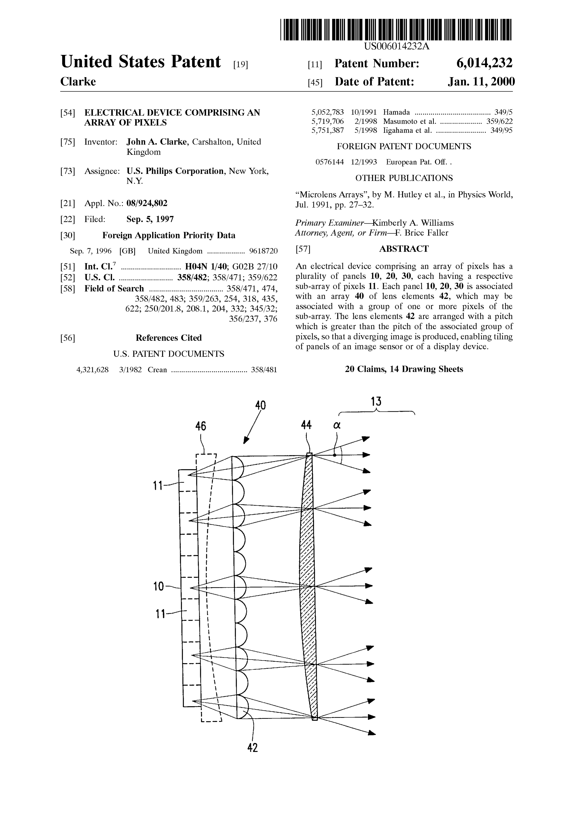
22 Filed: Sep. 5, 1997 Primary Examiner Kimberly A. Williams 30 Foreign Application Priority Data Attorney, Agent, or Firm-F. Brice Faller Sep. 7, 1996 GB United Kingdom ................... 96.1872O 57 ABSTRACT 51 Int. Cl." .............................. H04N 1/40; G02B 27/10 An electrical device comprising an array of pixels has a 52 U.S. Cl. ........................... 358/.482; 358/471; 359/622 plurality of panels 10, 20, 30, each having a respective 58 Field of Search ..................................... 358/471, 474, sub-array of pixels 11. Each panel 10, 20, 30 is associated 358/482, 483; 359/263, 254, 318, 435, with an array 40 of lens elements 42, which may be 622; 250/2018, 208.1, 204, 332: 345/32; asSociated with a group of one or more pixels of the 356/237, 376 Sub-array. The lens elements 42 are arranged with a pitch which is greater than the pitch of the associated group of 56) References Cited pixels, So that a diverging image is produced, enabling tiling of panels of an image Sensor or of a display device.
4.321,628 3/1982 Crean ...................................... 358/481 20 Claims, 14 Drawing Sheets
Page 2
Drawing sheet — no readable text.
Page 3
Drawing sheet — no readable text.
Page 4
Drawing sheet — no readable text.
Page 5
Drawing sheet — no readable text.
Page 6
Drawing sheet — no readable text.
Page 7
Drawing sheet — no readable text.
Page 8
Drawing sheet — no readable text.
Page 9
Drawing sheet — no readable text.
Page 10
Drawing sheet — no readable text.
Page 11
Drawing sheet — no readable text.
Page 12
Drawing sheet — no readable text.
Page 13
Drawing sheet — no readable text.
Page 14
Drawing sheet — no readable text.
Page 15
Drawing sheet — no readable text.
Page 16
ELECTRICAL DEVICE COMPRISING AN a significant distance between the array and the document to ARRAY OF PIXELS be sensed. Size constraints are, of course, equally important in the case of displays where the Overall depth of a display
BACKGROUND OF THE INVENTION panel is to be maintained as Small as possible. This invention relates to electrical devices having arrayS SUMMARY OF THE INVENTION of pixels, for example liquid crystal displayS or optical According to the present invention there is provided an image Sensors. The invention is particularly concerned with electrical device comprising an array of pixels, and having devices having arrays of pixels which are divided into a plurality of electrical panels, each panel providing a Sub-arrayS. respective Sub-array of pixels, an array of lens elements In order to make possible the manufacture of large area being associated with each panel. Each lens element is arrays, it is known to form a device from a plurality of asSociated with a group of one or more pixels of the Sub-arrays of pixels which are arranged beside each other in Sub-array, the lens elements being arranged with a pitch order to provide a large composite array. The known prob which is greater than the pitch of the associated groups of lem arises, both for image Sensors and for displays, that it is 15 pixels.
desirable to disguise the join between the Sub-arrayS. In accordance with the invention, a lens array is provided Generally, this may be achieved in one of two ways. One over each Sub-array of pixels, and the lens array covers a possibility is to use Sub-arrays which may be abutted greater area than the area of the Sub-array (by Virtue of the together, whilst maintaining a uniform pixel pitch acroSS the greater pitch). The general outline of the lens array is similar join. Obviously, this requires very accurate machining of the to the panel shape, for example a Square lens array over a Sub-arrays, particularly when the pixel dimensions are to be Square panel, or a rectangular lens array over a rectangular reduced to a minimum size, to increase the resolution of the panel.
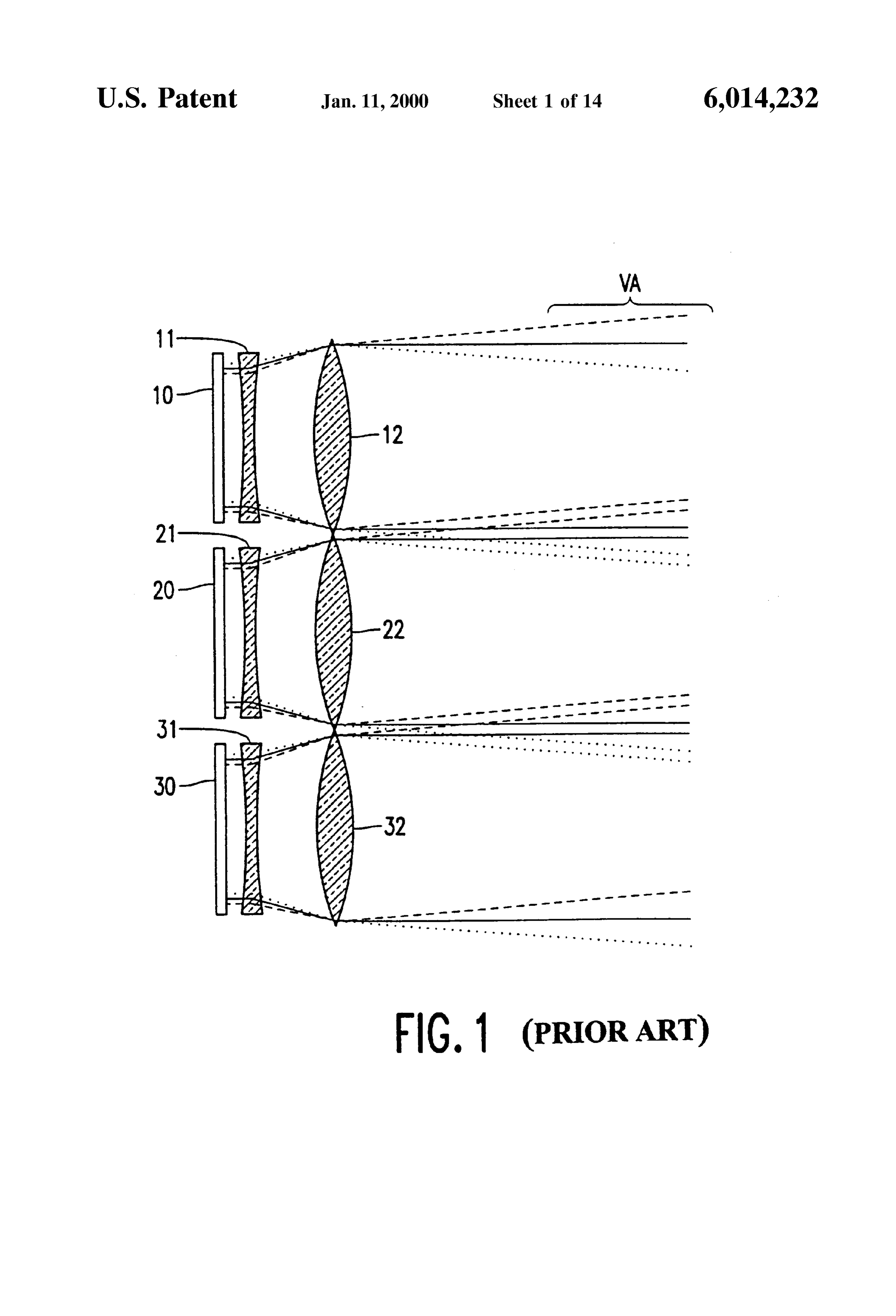
device. Also, electrical connections to peripheral circuitry The lens elements preferably comprise microlens ele can not be made along abutting edges, restricting the number ments. For example, a microlens may be associated with of Sub-arrays that can be used. The alternative possibility is 25 each pixel, in which case the pitch of the microlenses is to employ an optical System, which enables the Sub-arrays to greater than the pitch of the pixels. Alternatively, a microlens be slightly Spaced apart. The present invention concerns an may be associated with a group of pixels, for example a optical Solution to the problem of tiling a plurality of Square of nXn pixels. In this case, the pitch of the micro Sub-arrays to enable the manufacture of a larger array. lenses is greater than n times the pitch of the pixels. The The basic principle underlying the use of an optical “pitch of associated groups of pixels' as referred to above System to enable tiling of Sub-arrayS is that the optical and in the following description and claims is intended to System should provide an optical enlargement of each Sub indicate n times the individual pixel pitch, where the group array, So that the image of the Sub-arrays produced by the of pixels has a dimension of n pixels. Although described as optical System constitutes a uniform image, and the joins Square, the group of pixels could be rectangular, hexagonal between the sub-arrays have been eliminated. In other 35 or Some other shape. The value of n, when referring to a words, in the case of a display, an enlarged view of the dimension of n pixels, does not have to be an integer. Sub-arrayS is viewed, and in the case of an image Sensor, the The greater pitch of the lens elements results in the image to be Sensed is divided into portions which are microlens array thereby receiving a diverging image from reduced in size for Sensing by the Sub-arrayS. the Sub-array of pixels (or producing a converging image to This basic concept of optical enlargement could, for 40 the Sub-array of pixels). This gives rise to a focused real example, Suggest the use of the arrangement employed in a image of the Sub-array which is greater in Size than the Galilean telescope, as represented Schematically in FIG. 1. Sub-array, thereby enabling tiling to form a large area Three sub-arrays are represented as 10, 20 and 30, each imaging or display device.
having an associated diverging lens 11, 21, 31 and an Each panel may comprise a converging field lens associ asSociated converging lens 12, 22, 32. Such an arrangement 45 ated with all pixels of the sub-array, the field lenses of can maintain parallel beams at the output of the converging adjacent panels Substantially abutting one another, and hav lenses, whilst providing enlargement. However, the image ing the same general shape as the respective panel, for Seen from the viewing area VA is an enlarged virtual image example a Square field lens associated with a Square panel. of each sub-array 10, 20, 30. For a display, this presents the This enables the light beams incident upon, or emitted by, problem that the range of viewing angles may be limited, 50 each pixel of the Sub-array to travel Substantially perpen because viewing from different angles will result in Some dicularly to the plane of the Sub-array in the active area of loSS of the image at the boundaries, Since these images are the device. For the purposes of this description, the active Virtual and may be partially hidden by the lens apertures. In area is defined as the viewing area of a display, or the area the case of an image Sensor, imaging must take place at the in which a document to be imaged is positioned for an image real optical focus of the optical System, So the arrangement 55 SCSO.
of FIG. 1 will only work if a supplementary optical system The microlens array and the respective field lens may be is provided to image the document at the Virtual image combined as a single unit, by providing the array of lens plane. elements on a face of the field lens. U.S. Pat. No. 4,321,628 discloses an image scanning A diverging lens may be provided adjacent each panel System in which a linear array of photoSensitive elements is 60 between the respective panel and the lens array, and asso divided into Sub-arrays which are Spaced apart. Each Sub ciated with all pixels of the sub-array. This ensures that light array is associated with a pair of converging lenses which is incident to, or emitted from, each pixel Substantially effectively focus a non-inverted image of the Sub-array onto normally or at the same angle. This gives better contrast in a platen 10, where a document can be placed for Scanning. the case of a display, and improved light collection in the The sensor arrangement of U.S. Pat. No. 4,321,628 requires 65 case of an image Sensor.
converging lenses of Sufficient power to produce a focused A non-inverting lens arrangement may be associated with image of each entire Sub-array at the platen, and this imposes each panel, the non-inverting lens arrangement including the
Page 17
lens array and at least one further lens array, the lens tinuous image in the active area 13 may be Scaled down by elements of the lens array and the at least one further lens the optical System to enable these portions to be Sensed by array being arranged with different pitches, each greater than different Spaced image Sensing panels. the pitch of the associated group of pixels. The use of a In general terms, the invention provides a lens array 40 non-inverting lens arrangement Simplifies the alignment of asSociated with the Sub-array of pixels of each panel 10, and the lens arrangement with the panels. which comprises an array of individual lens elements 42. AS described above, the electrical device of the invention The lens elements may comprise shaped microlenses. may comprise a display or an image Sensor. In either case, However, other forms of Small Scale converging lens ele each lens element is preferably associated with a plurality of ment may be employed, for example graded-indeX lenses pixels. Each panel may comprise a further array of lens (which rely upon non-uniform refractive index within the elements arranged Such that light incident on or emitted by lens element instead of relying upon the shape of the each pixel of the panel is Substantially telecentric in the boundary between media of different refractive indices). It is active area of the device. This enables light beams associ equally possible to fabricate arrays of holographic lenses or ated with each pixel to project perpendicularly to the plane of diffractive elements. These possibilities will all be evident of the Sub-array, in the active area of the device. 15 to those skilled in the art.
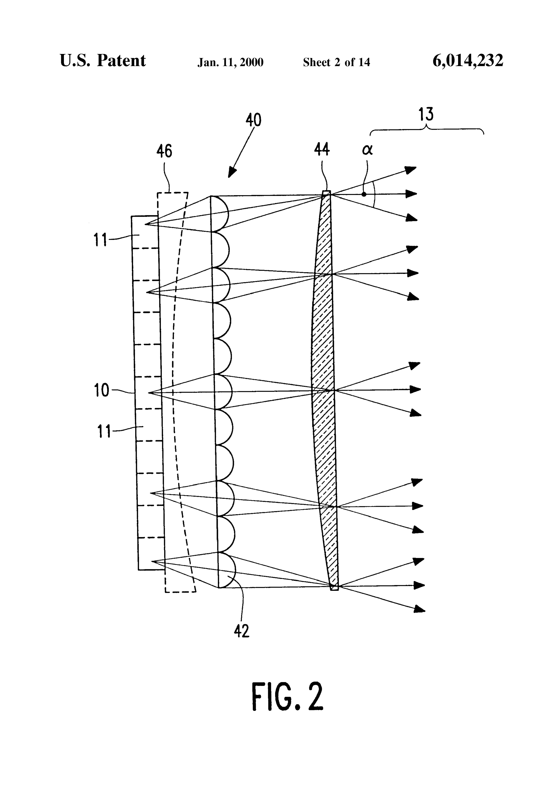
The lens elements of the lens array may have a diameter In the example shown in FIG.2, each microlens 42 can be Substantially corresponding to their pitch, So that the lens considered to be associated with an individual pixel 11 of the elements Substantially abut one another. This is preferred Sub-array. The pitch of the microlenses 42 is slightly greater with displays, where a large field of view is desired. A than the pitch of the pixels 11, Such that the microlens array diffusing Surface may also be included to increase the field 40 occupies a greater area than the area of the Sub-array. The of view. spacing of the microlens array 40 from the Sub-array and the However, for image Sensors, the diameter of the lens spacing from the active area are Selected according to the elements may be less than the pitch of lens elements with at focal length of each microlens element 42, in Such a way that least a portion of the Space between the lens elements being 25 an image of each pixel is produced by the optical System at filled with opaque material. Thus, the open aperture of each the Surface of the display or at the Surface where a document lens element may be reduced, and this has the advantage of to be imaged is positioned. It is preferred that the local improving the depth of focus for an image Sensor, for enlargement of each pixel by the microlenses corresponds to example in document Scanning applications. the global enlargement of the entire Sub-array by virtue of In addition, means may be provided for blocking the the is pitch of the microlenses. The single microlens array 40
Sufficient, to provide the required focusing and enlarge passage of light between each pixel and regions of the active ment of the image of the Sub-array to enable tiling of display area other than a region associated with the respective pixel. or image Sensor Sub-arrayS.
This avoids the appearance of ghost images in a captured image, or improves the quality of a displayed image. This An additional factor influencing the desired local magni means may comprise blocking arrangements of opaque 35 fication produced by the microlenses 42 is the “open area’ material, and/or aperture arrayS. of the pixels. If the light responsive portion of a pixel 11 occupies a relatively Small area, compared to the area of the
BRIEF DESCRIPTION OF THE DRAWINGS panel 10 associated with that pixel, then an increased magnification of the microlenses 42 may be desirable So that
FIG. 1 shows a conventional telescope arrangement for the output of the display is continuous, or an image Sensor optical enlargement, the arrangement being applied to Sub 40 receives Signals representing the entire image to be Sensed. arrayS,
Microlens arrays are known, and the microlens array used
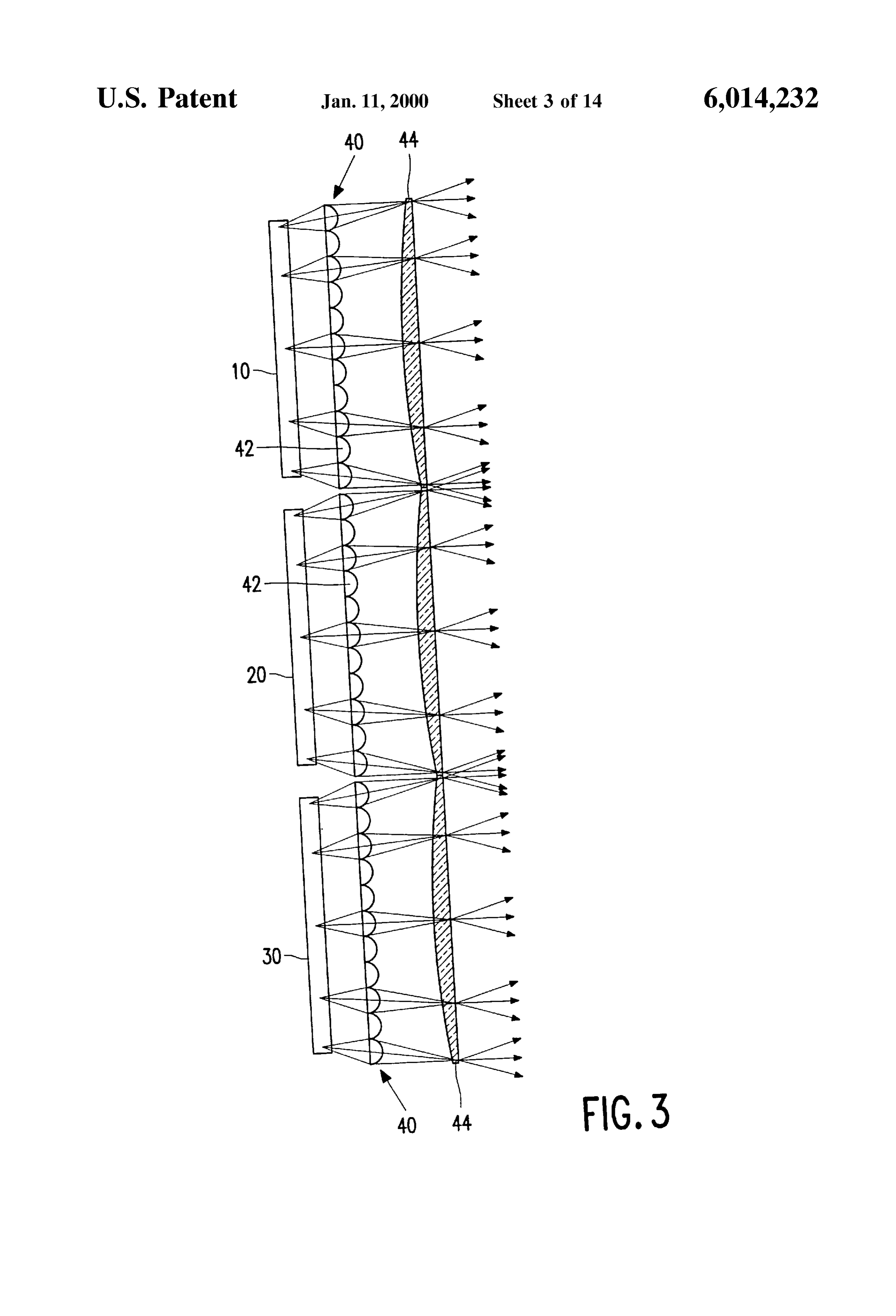
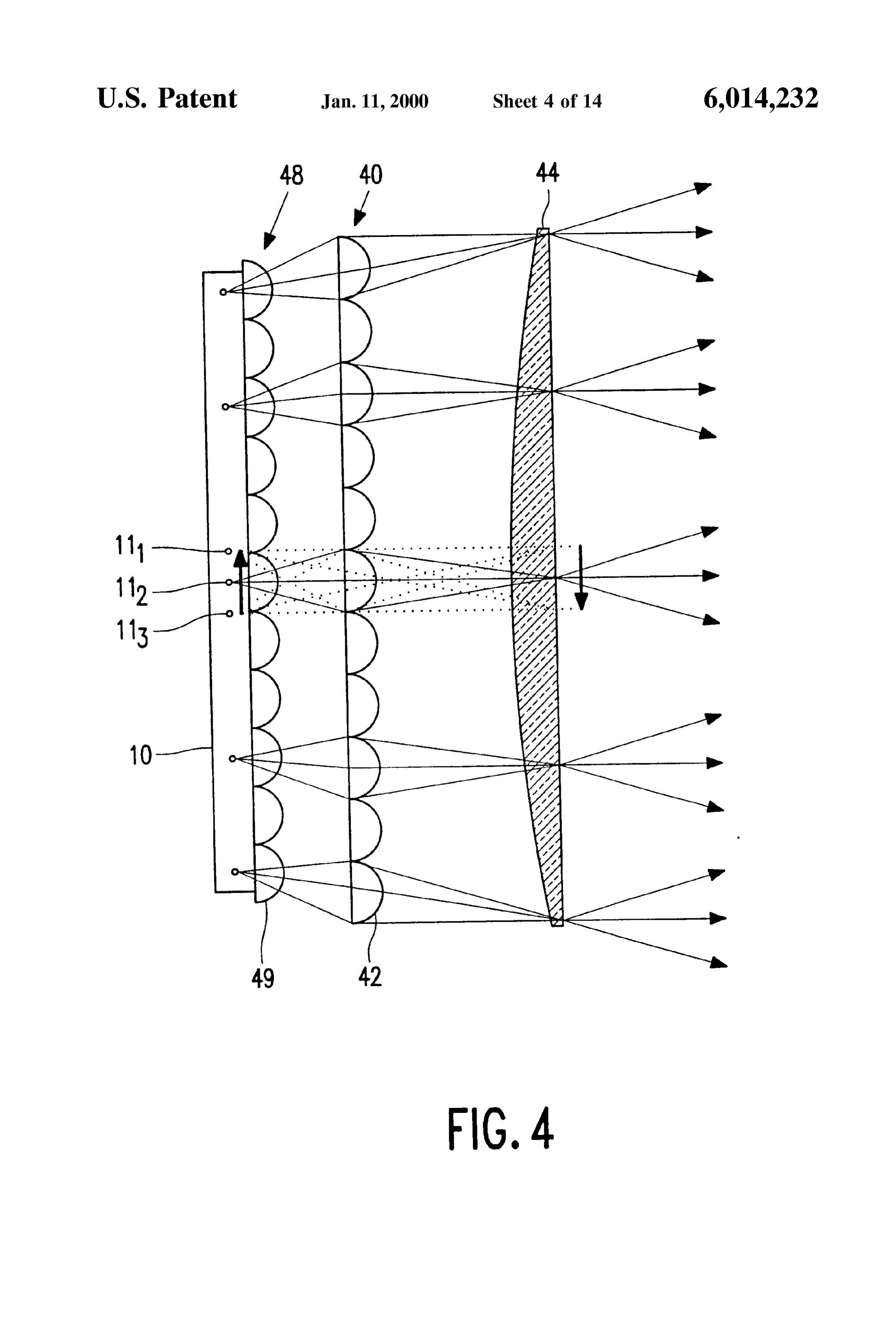
FIG. 2 shows a panel and associated optical arrangement in the present invention may be formed by known tech of an electrical device according to the invention; niques. The precise technique to be adopted will depend FIG. 3 shows a device according to the invention com 45 upon the size of the microlens elements to be adopted. prising three of the panels of FIG. 2; and If a microlens is to be associated with each pixel, Very FIGS. 4 to 14 show various modifications to the optical Small microlenses are required. In Such a case, it is known arrangement associated with each panel. to form shaped lens elements of diameter as low as 50 um
DETAILED DESCRIPTION OF THE
from reformed thermoplastic resin. For this purpose, a
PREFERRED EMBODIMENTS 50 Substrate of the array 40 (usually glass) is coated with a thermoplastic resin layer, which may be applied by means of
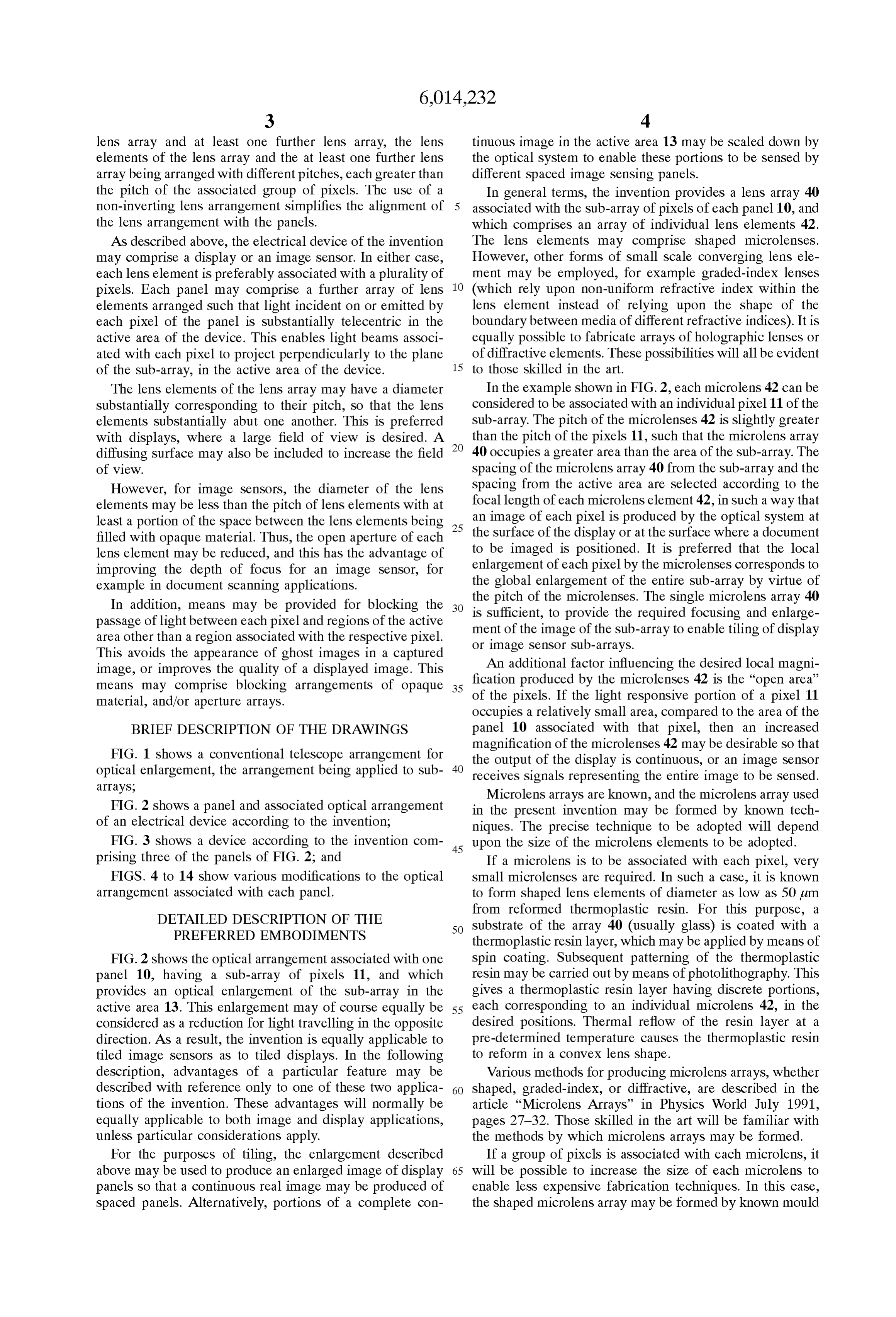
FIG. 2 shows the optical arrangement associated with one Spin coating. Subsequent patterning of the thermoplastic panel 10, having a Sub-array of pixels 11, and which resin may be carried out by means of photolithography. This provides an optical enlargement of the Sub-array in the gives a thermoplastic resin layer having discrete portions, active area 13. This enlargement may of course equally be 55 each corresponding to an individual microlens 42, in the considered as a reduction for light travelling in the opposite desired positions. Thermal reflow of the resin layer at a direction. As a result, the invention is equally applicable to pre-determined temperature causes the thermoplastic resin tiled image Sensors as to tiled displayS. In the following to reform in a convex lens shape.
description, advantages of a particular feature may be Various methods for producing microlens arrays, whether described with reference only to one of these two applica 60 shaped, graded-index, or diffractive, are described in the tions of the invention. These advantages will normally be article “Microlens Arrays” in Physics World July 1991, equally applicable to both image and display applications, pages 27–32. Those skilled in the art will be familiar with unless particular considerations apply. the methods by which microlens arrays may be formed. For the purposes of tiling, the enlargement described If a group of pixels is associated with each microlens, it above may be used to produce an enlarged image of display 65 will be possible to increase the Size of each microlens to panels So that a continuous real image may be produced of enable leSS expensive fabrication techniques. In this case, Spaced panels. Alternatively, portions of a complete con the shaped microlens array may be formed by known mould
Page 18
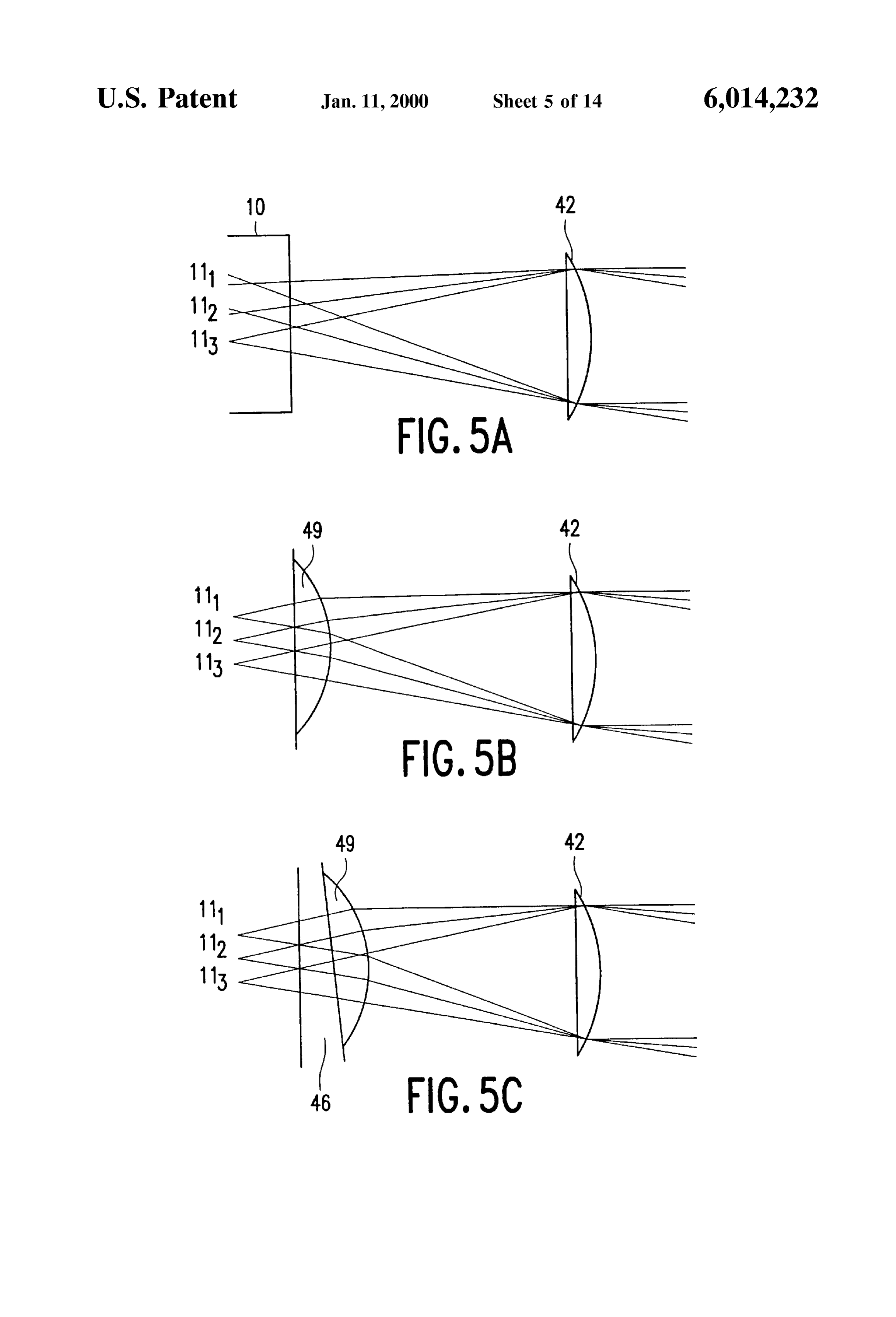
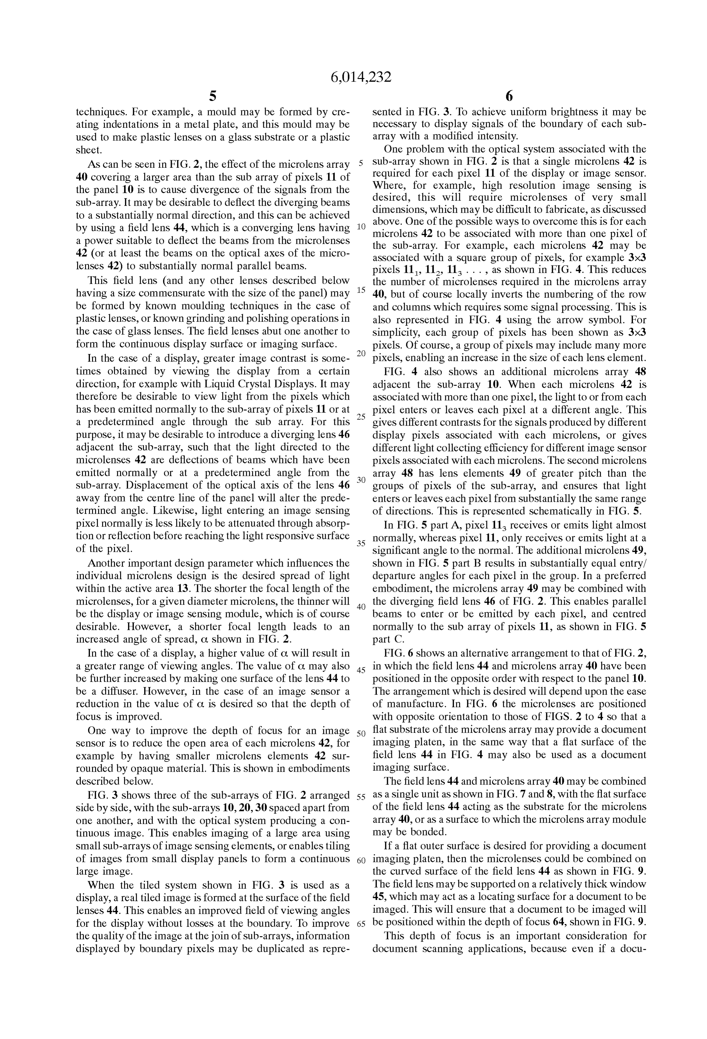
S 6 techniques. For example, a mould may be formed by cre sented in FIG. 3. To achieve uniform brightness it may be ating indentations in a metal plate, and this mould may be necessary to display Signals of the boundary of each Sub used to make plastic lenses on a glass Substrate or a plastic array with a modified intensity. sheet. One problem with the optical system associated with the As can be seen in FIG. 2, the effect of the microlens array sub-array shown in FIG. 2 is that a single microlens 42 is 40 covering a larger area than the Sub array of pixels 11 of required for each pixel 11 of the display or image Sensor. the panel 10 is to cause divergence of the Signals from the Where, for example, high resolution image Sensing is Sub-array. It may be desirable to deflect the diverging beams desired, this will require microlenses of very Small to a Substantially normal direction, and this can be achieved dimensions, which may be difficult to fabricate, as discussed above. One of the possible ways to overcome this is for each by using a field lens 44, which is a converging lens having microlens 42 to be associated with more than one pixel of a power Suitable to deflect the beams from the microlenses the Sub-array. For example, each microlens 42 may be 42 (or at least the beams on the optical axes of the micro asSociated with a Square group of pixels, for example 3x3 lenses 42) to Substantially normal parallel beams. pixels 11, 11, 11 . . . , as shown in FIG. 4. This reduces This field lens (and any other lenses described below 15 the number of microlenses required in the microlens array having a size commensurate with the size of the panel) may 40, but of course locally inverts the numbering of the row be formed by known moulding techniques in the case of and columns which requires Some Signal processing. This is plastic lenses, or known grinding and polishing operations in also represented in FIG. 4 using the arrow symbol. For the case of glass lenses. The field lenses abut one another to Simplicity, each group of pixels has been shown as 3x3 form the continuous display Surface or imaging Surface. pixels. Of course, a group of pixels may include many more In the case of a display, greater image contrast is Some pixels, enabling an increase in the size of each lens element. times obtained by Viewing the display from a certain FIG. 4 also shows an additional microlens array 48 direction, for example with Liquid Crystal DisplayS. It may adjacent the sub-array 10. When each microlens 42 is therefore be desirable to view light from the pixels which asSociated with more than one pixel, the light to or from each has been emitted normally to the sub-array of pixels 11 or at 25 pixel enters or leaves each pixel at a different angle. This a predetermined angle through the Sub array. For this gives different contrasts for the Signals produced by different purpose, it may be desirable to introduce a diverging lens 46 display pixels associated with each microlens, or gives adjacent the Sub-array, Such that the light directed to the different light collecting efficiency for different image Sensor microlenses 42 are deflections of beams which have been pixels associated with each microlens. The Second microlens emitted normally or at a predetermined angle from the array 48 has lens elements 49 of greater pitch than the sub-array. Displacement of the optical axis of the lens 46 groups of pixels of the Sub-array, and ensures that light away from the centre line of the panel will alter the prede enters or leaves each pixel from Substantially the same range termined angle. Likewise, light entering an image Sensing of directions. This is represented schematically in FIG. 5. pixel normally is less likely to be attenuated through absorp In FIG. 5 part A, pixel 11 receives or emits light almost tion or reflection before reaching the light responsive Surface 35 normally, whereas pixel 11, only receives or emits light at a of the pixel. Significant angle to the normal. The additional microlens 49, Another important design parameter which influences the shown in FIG. 5 part B results in Substantially equal entry/ individual microlens design is the desired spread of light departure angles for each pixel in the group. In a preferred within the active area 13. The shorter the focal length of the embodiment, the microlens array 49 may be combined with microlenses, for a given diameter microlens, the thinner will 40 the diverging field lens 46 of FIG. 2. This enables parallel be the display or image Sensing module, which is of course beams to enter or be emitted by each pixel, and centred desirable. However, a shorter focal length leads to an normally to the Sub array of pixels 11, as shown in FIG. 5 increased angle of Spread, C. Shown in FIG. 2. part C.
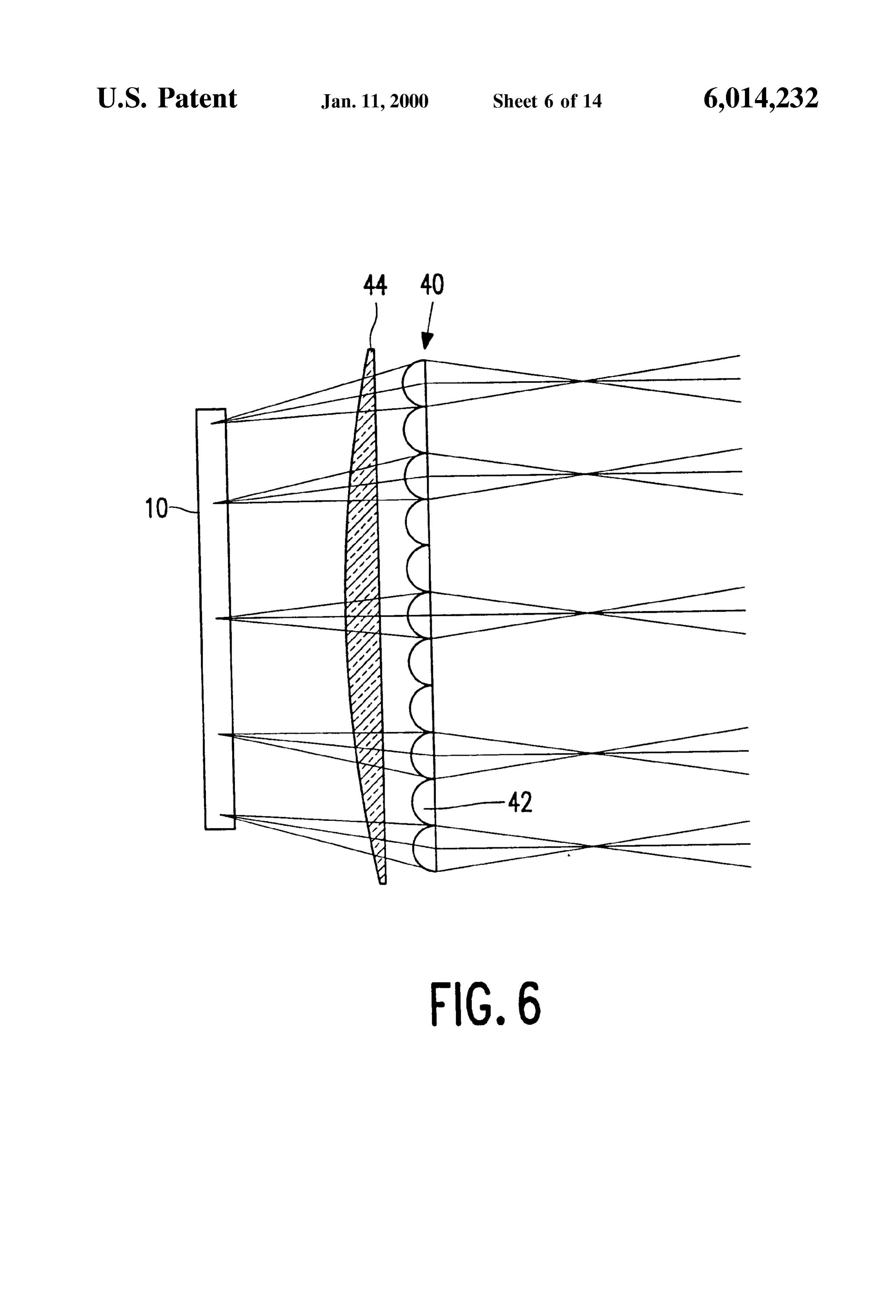
In the case of a display, a higher value of C. will result in FIG. 6 shows an alternative arrangement to that of FIG. 2, a greater range of viewing angles. The value of C. may also 45 in which the field lens 44 and microlens array 40 have been be further increased by making one Surface of the lens 44 to positioned in the opposite order with respect to the panel 10. be a diffuser. However, in the case of an image Sensor a The arrangement which is desired will depend upon the ease reduction in the value of C. is desired so that the depth of of manufacture. In FIG. 6 the microlenses are positioned focus is improved. with opposite orientation to those of FIGS. 2 to 4 so that a One way to improve the depth of focus for an image 50 flat Substrate of the microlens array may provide a document Sensor is to reduce the open area of each microlens 42, for imaging platen, in the same way that a flat Surface of the example by having Smaller microlens elements 42 Sur field lens 44 in FIG. 4 may also be used as a document rounded by opaque material. This is shown in embodiments imaging Surface.
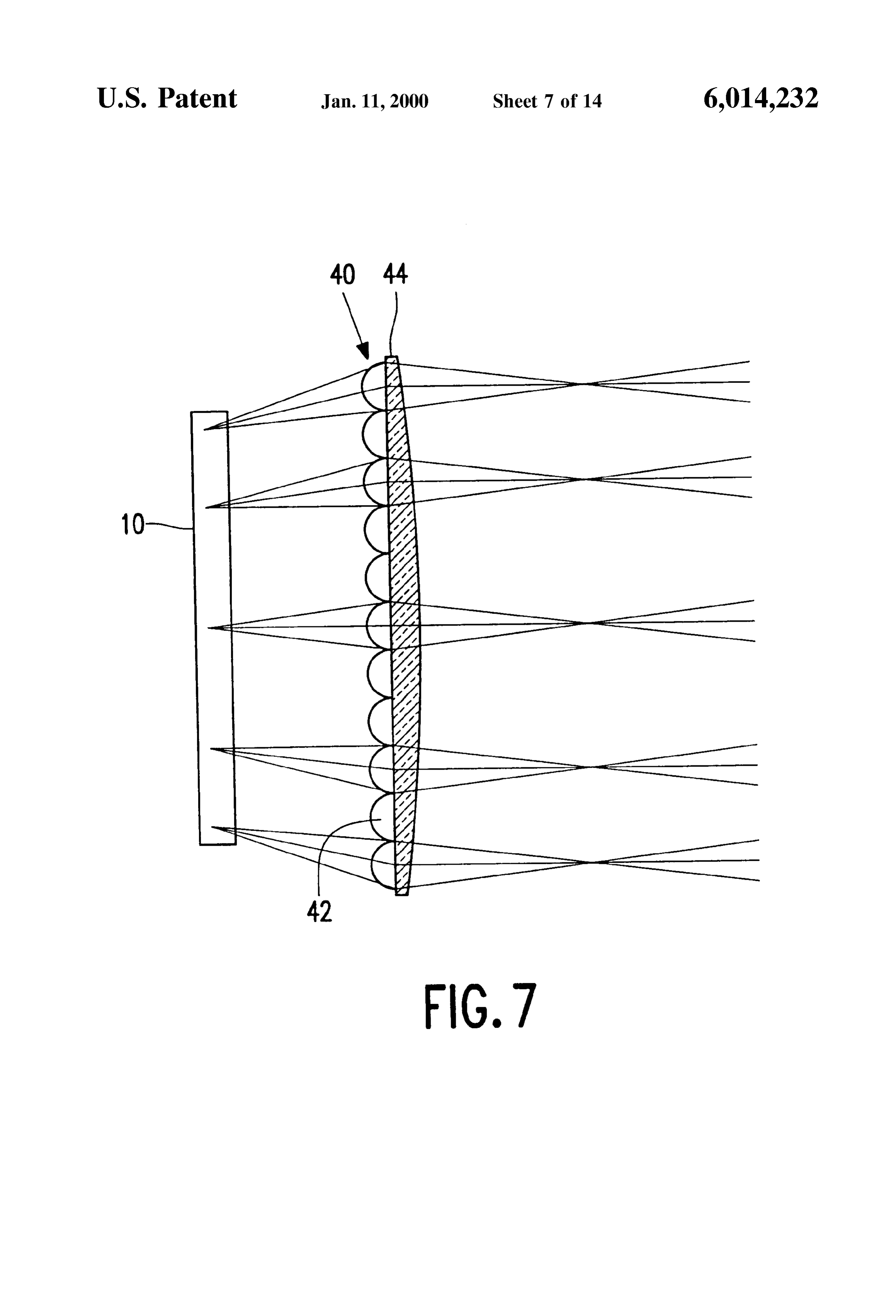
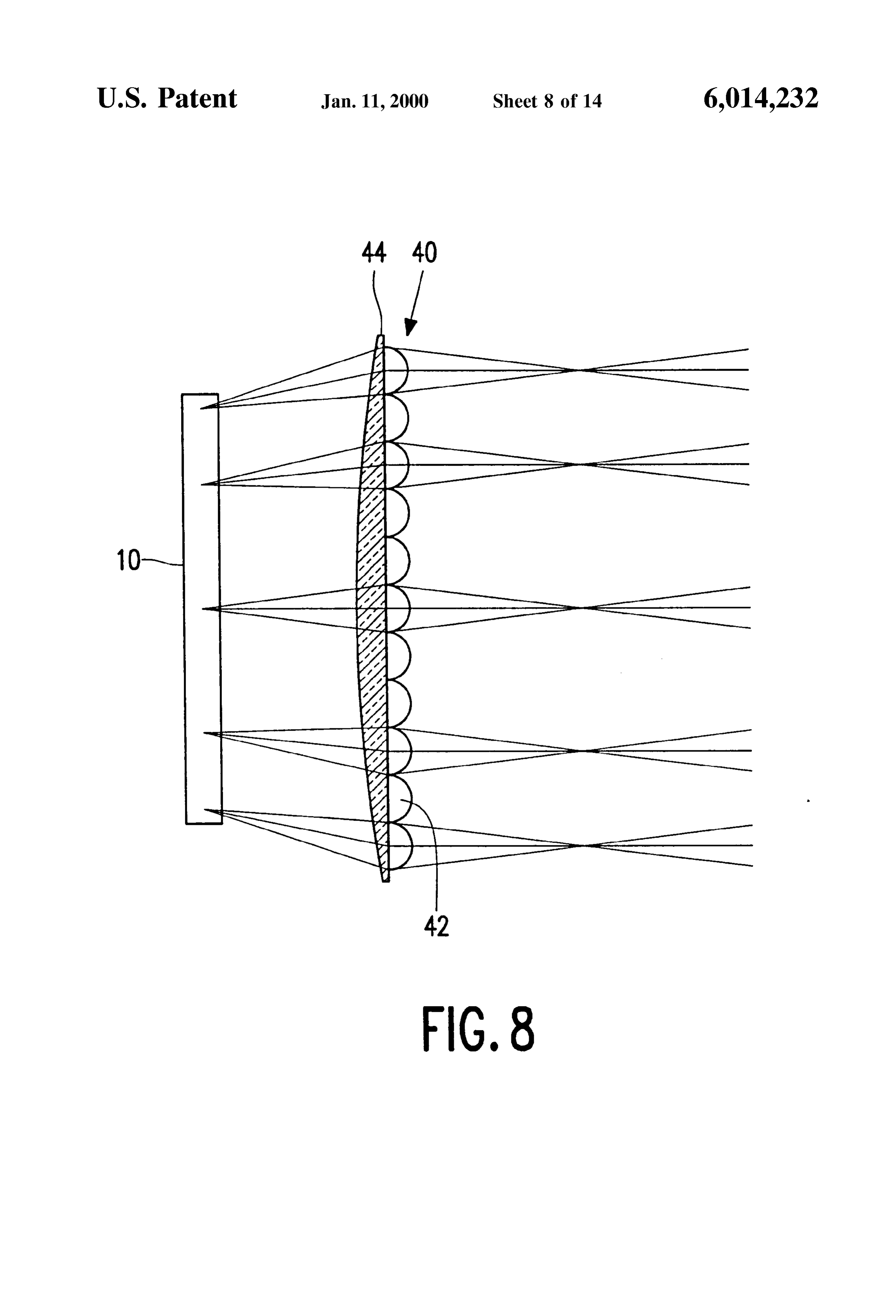
described below. The field lens 44 and microlens array 40 may be combined FIG. 3 shows three of the Sub-arrays of FIG. 2 arranged 55 as a single unit as shown in FIG. 7 and 8, with the flat surface side by side, with the sub-arrays 10, 20, 30 spaced apart from of the field lens 44 acting as the Substrate for the microlens one another, and with the optical System producing a con array 40, or as a Surface to which the microlens array module tinuous image. This enables imaging of a large area using may be bonded.
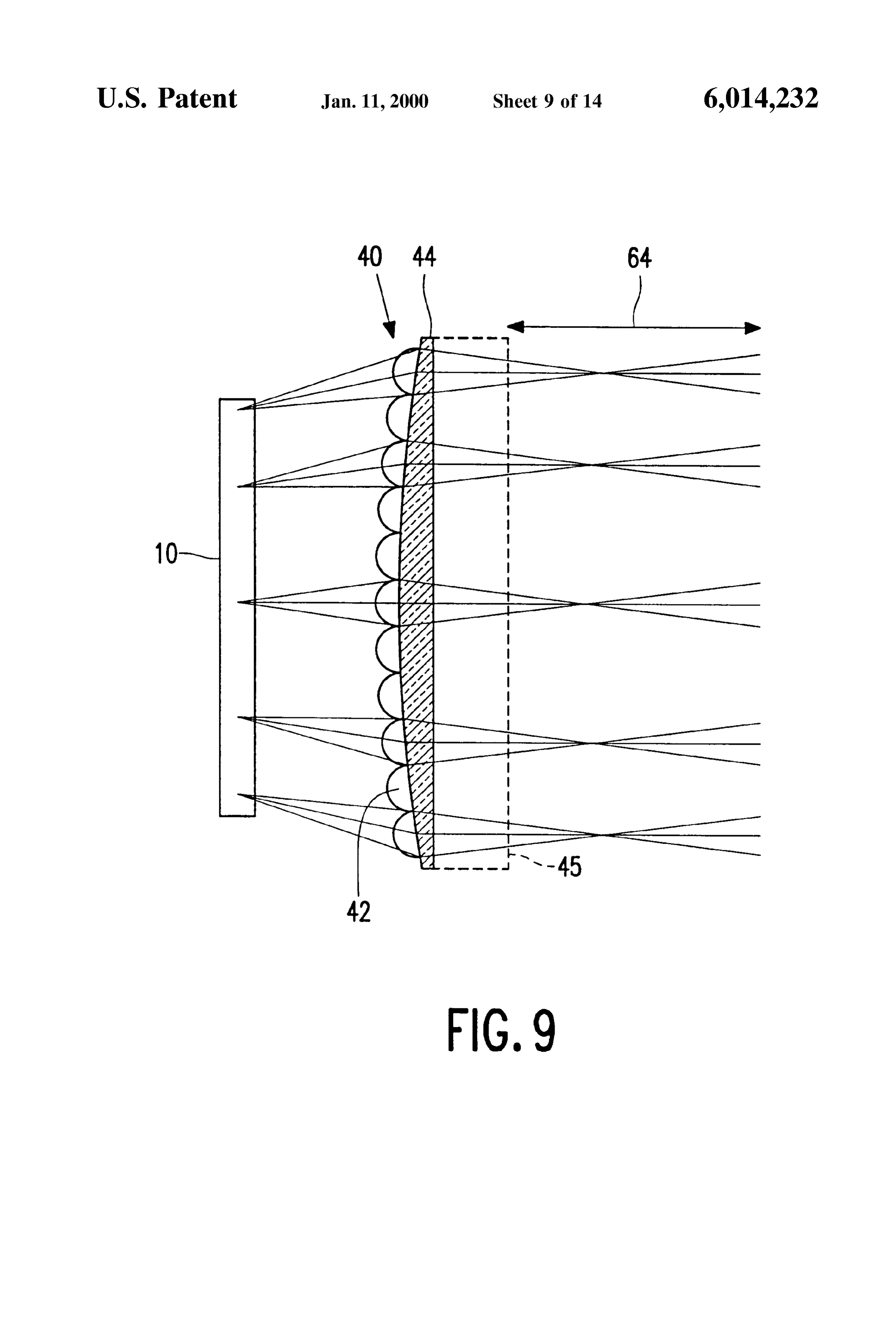
Small Sub-arrays of image Sensing elements, or enables tiling If a flat Outer Surface is desired for providing a document of images from Small display panels to form a continuous 60 imaging platen, then the microlenses could be combined on large image. the curved Surface of the field lens 44 as shown in FIG. 9. When the tiled system shown in FIG. 3 is used as a The field lens may be supported on a relatively thick window display, a real tiled image is formed at the Surface of the field 45, which may act as a locating Surface for a document to be lenses 44. This enables an improved field of Viewing angles imaged. This will ensure that a document to be imaged will for the display without losses at the boundary. To improve 65 be positioned within the depth of focus 64, shown in FIG. 9. the quality of the image at the join of Sub-arrays, information This depth of focus is an important consideration for displayed by boundary pixels may be duplicated as repre document Scanning applications, because even if a docu
Page 19
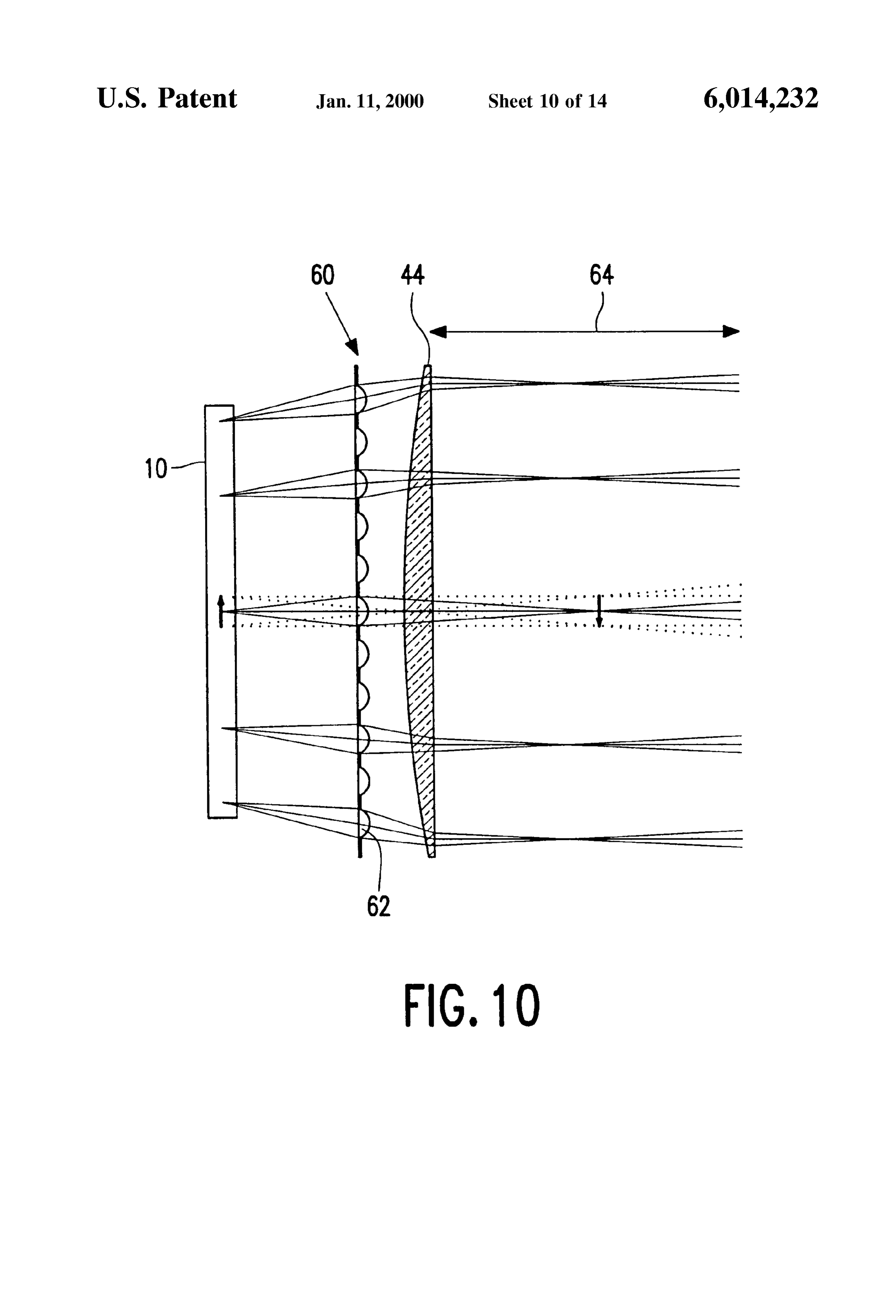
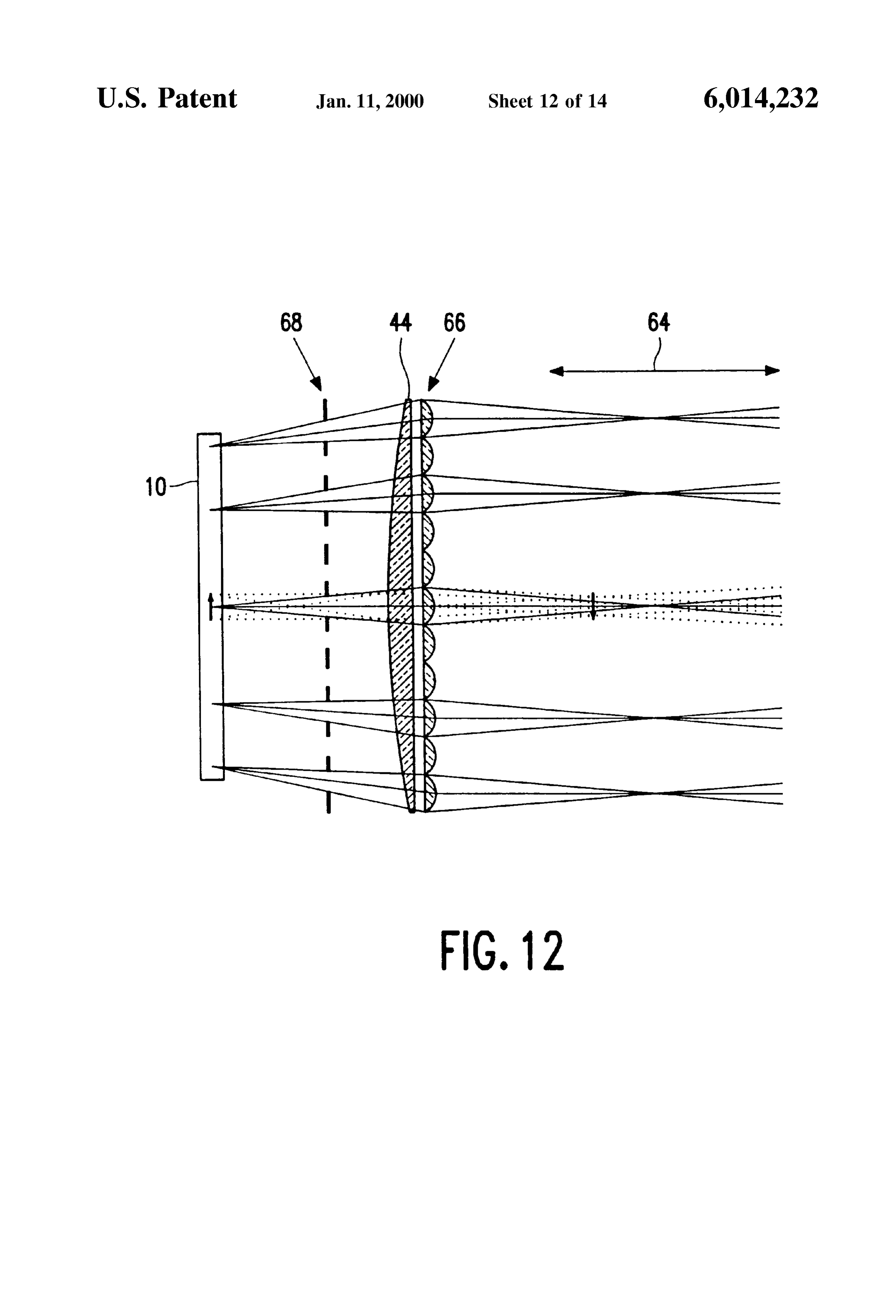
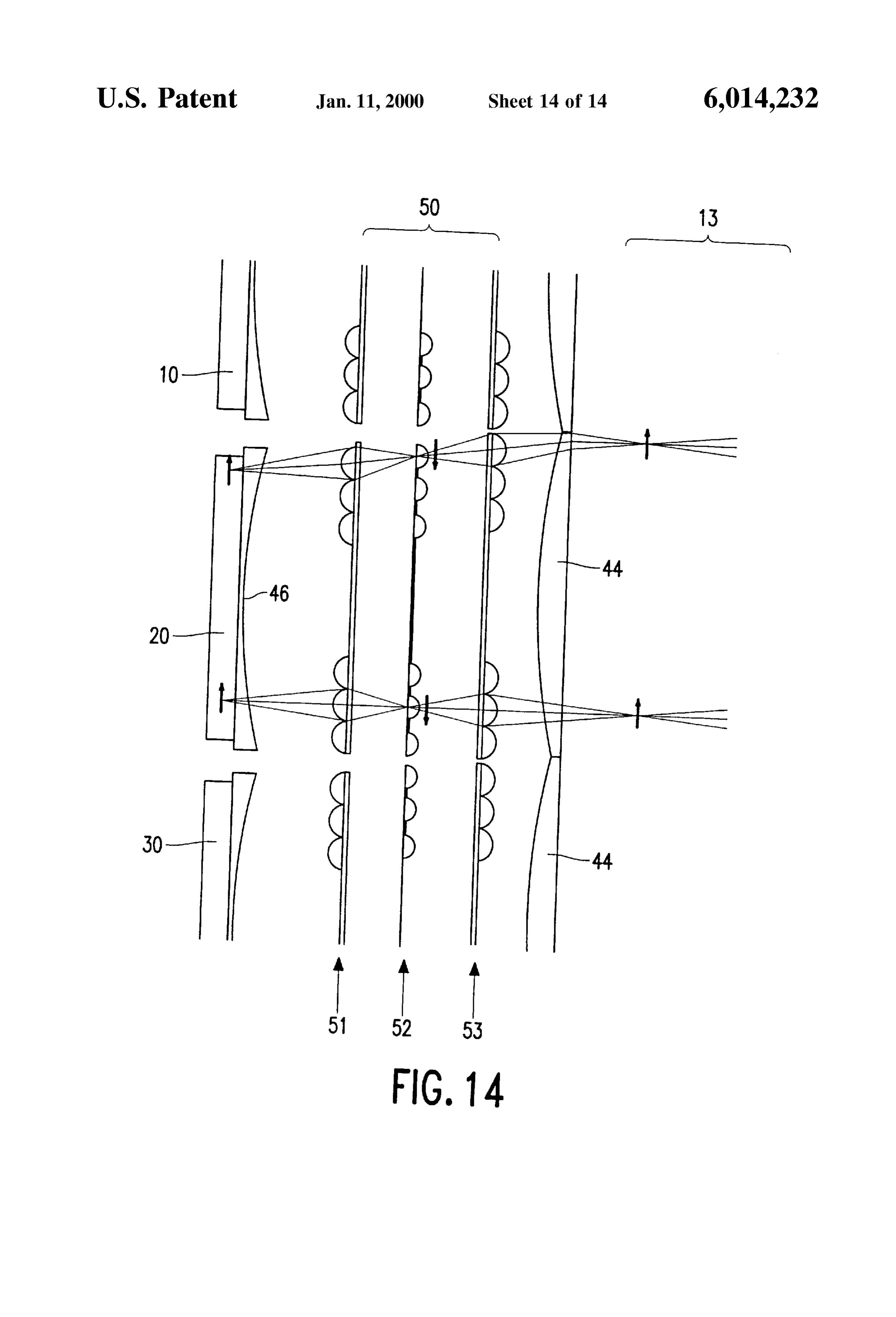
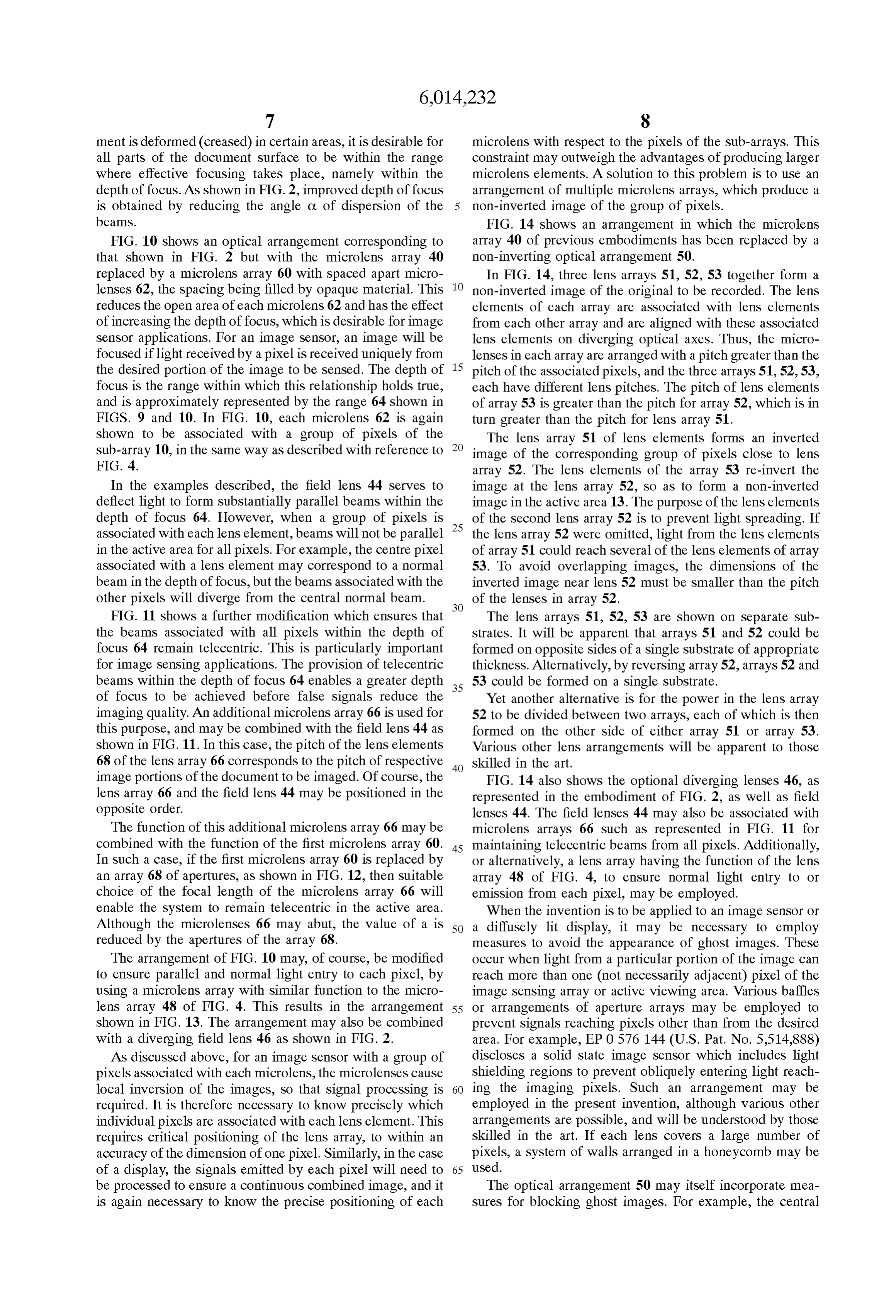
ment is deformed (creased) in certain areas, it is desirable for microlens with respect to the pixels of the Sub-arrayS. This all parts of the document Surface to be within the range constraint may outweigh the advantages of producing larger where effective focusing takes place, namely within the microlens elements. A Solution to this problem is to use an depth of focus. As shown in FIG. 2, improved depth of focus arrangement of multiple microlens arrays, which produce a is obtained by reducing the angle C. of dispersion of the non-inverted image of the group of pixels. beams. FIG. 14 shows an arrangement in which the microlens FIG. 10 shows an optical arrangement corresponding to array 40 of previous embodiments has been replaced by a that shown in FIG. 2 but with the microlens array 40 non-inverting optical arrangement 50.
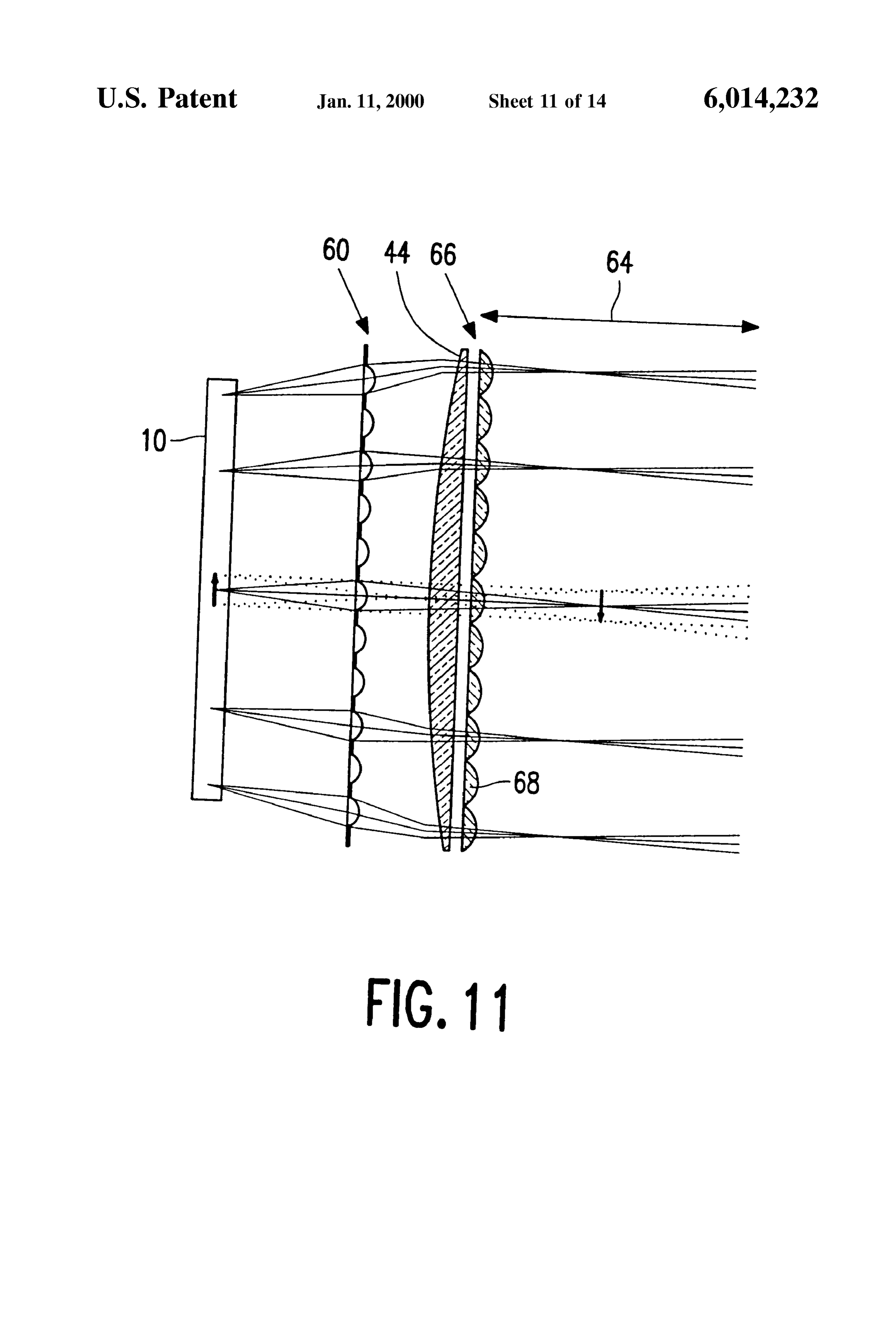
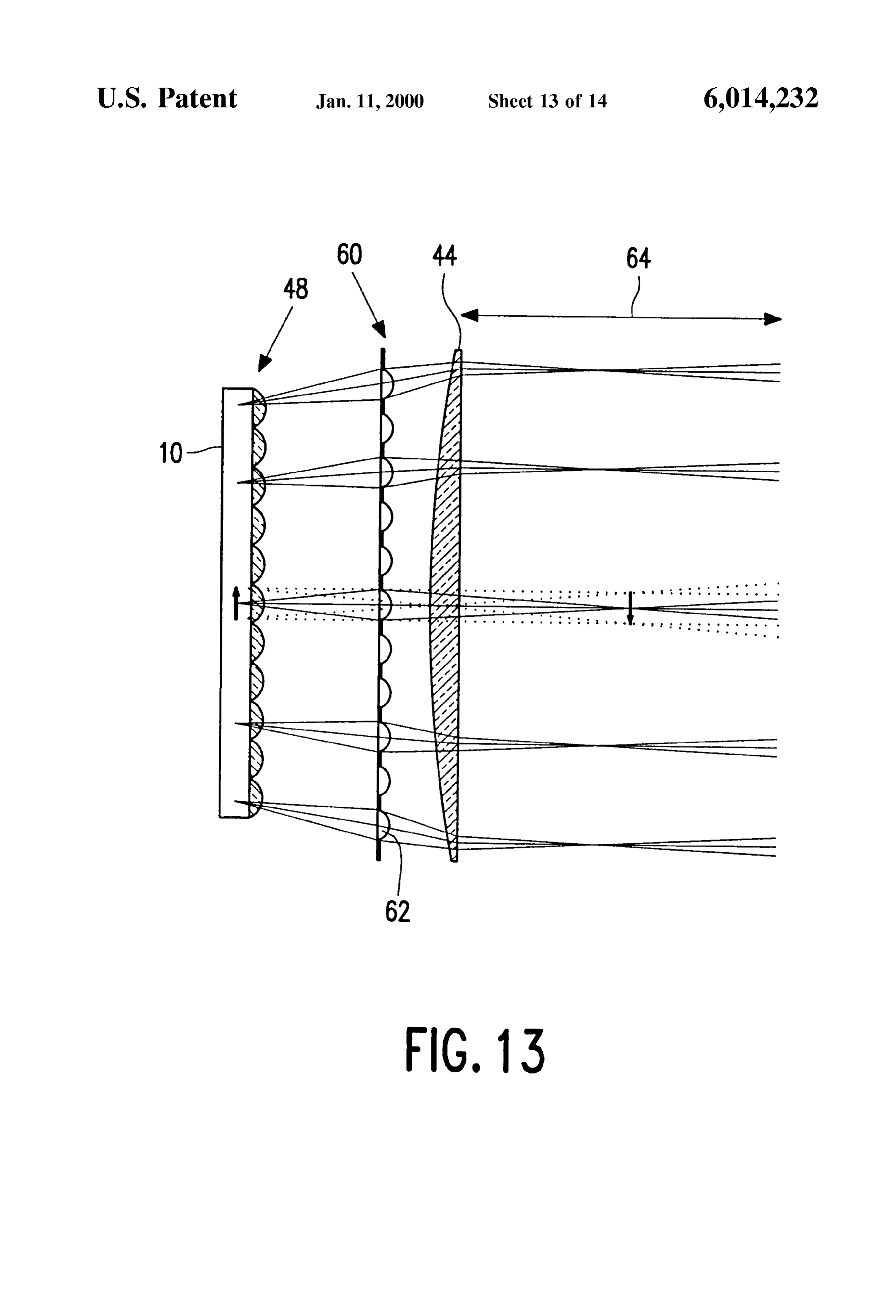
replaced by a microlens array 60 with Spaced apart micro In FIG. 14, three lens arrays 51, 52, 53 together form a lenses 62, the Spacing being filled by opaque material. This non-inverted image of the original to be recorded. The lens reduces the open area of each microlens 62 and has the effect elements of each array are associated with lens elements of increasing the depth of focus, which is desirable for image from each other array and are aligned with these associated Sensor applications. For an image Sensor, an image will be lens elements on diverging optical axes. Thus, the micro focused if light received by a pixel is received uniquely from lenses in each array are arranged with a pitch greater than the the desired portion of the image to be sensed. The depth of 15 pitch of the associated pixels, and the three arrays 51, 52, 53, focus is the range within which this relationship holds true, each have different lens pitches. The pitch of lens elements and is approximately represented by the range 64 shown in of array 53 is greater than the pitch for array 52, which is in FIGS. 9 and 10. In FIG. 10, each microlens 62 is again turn greater than the pitch for lens array 51. shown to be associated with a group of pixels of the The lens array 51 of lens elements forms an inverted sub-array 10, in the same way as described with reference to image of the corresponding group of pixels close to lens FIG. 4. array 52. The lens elements of the array 53 re-invert the In the examples described, the field lens 44 serves to image at the lens array 52, So as to form a non-inverted deflect light to form substantially parallel beams within the image in the active area 13. The purpose of the lens elements depth of focus 64. However, when a group of pixels is 25 of the Second lens array 52 is to prevent light spreading. If asSociated with each lens element, beams will not be parallel the lens array 52 were omitted, light from the lens elements in the active area for all pixels. For example, the centre pixel of array 51 could reach several of the lens elements of array asSociated with a lens element may correspond to a normal 53. To avoid overlapping images, the dimensions of the beam in the depth of focus, but the beams associated with the inverted image near lens 52 must be Smaller than the pitch other pixels will diverge from the central normal beam. of the lenses in array 52.
FIG. 11 shows a further modification which ensures that The lens arrays 51, 52, 53 are shown on separate Sub the beams associated with all pixels within the depth of strates. It will be apparent that arrays 51 and 52 could be focus 64 remain telecentric. This is particularly important formed on opposite Sides of a single Substrate of appropriate for image Sensing applications. The provision of telecentric thickness. Alternatively, by reversing array 52, arrayS 52 and beams within the depth of focus 64 enables a greater depth 35 53 could be formed on a single substrate. of focus to be achieved before false signals reduce the Yet another alternative is for the power in the lens array imaging quality. An additional microlens array 66 is used for 52 to be divided between two arrays, each of which is then this purpose, and may be combined with the field lens 44 as formed on the other side of either array 51 or array 53. shown in FIG. 11. In this case, the pitch of the lens elements Various other lens arrangements will be apparent to those 68 of the lens array 66 corresponds to the pitch of respective 40 skilled in the art.
image portions of the document to be imaged. Of course, the FIG. 14 also shows the optional diverging lenses 46, as lens array 66 and the field lens 44 may be positioned in the represented in the embodiment of FIG. 2, as well as field opposite order. lenses 44. The field lenses 44 may also be associated with The function of this additional microlens array 66 may be microlens arrays 66 Such as represented in FIG. 11 for combined with the function of the first microlens array 60. 45 maintaining telecentric beams from all pixels. Additionally, In such a case, if the first microlens array 60 is replaced by or alternatively, a lens array having the function of the lens an array 68 of apertures, as shown in FIG. 12, then suitable array 48 of FIG. 4, to ensure normal light entry to or choice of the focal length of the microlens array 66 will emission from each pixel, may be employed. enable the System to remain telecentric in the active area. When the invention is to be applied to an image Sensor or Although the microlenses 66 may abut, the value of a is 50 a diffusely lit display, it may be necessary to employ reduced by the apertures of the array 68. measures to avoid the appearance of ghost images. These The arrangement of FIG. 10 may, of course, be modified occur when light from a particular portion of the image can to ensure parallel and normal light entry to each pixel, by reach more than one (not necessarily adjacent) pixel of the using a microlens array with Similar function to the micro image Sensing array or active viewing area. Various baffles lens array 48 of FIG. 4. This results in the arrangement 55 or arrangements of aperture arrayS may be employed to shown in FIG. 13. The arrangement may also be combined prevent Signals reaching pixels other than from the desired with a diverging field lens 46 as shown in FIG. 2. area. For example, EP 0576 144 (U.S. Pat. No. 5,514,888) AS discussed above, for an image Sensor with a group of discloses a Solid State image Sensor which includes light pixels associated with each microlens, the microlenses cause Shielding regions to prevent obliquely entering light reach local inversion of the images, So that signal processing is 60 ing the imaging pixels. Such an arrangement may be required. It is therefore necessary to know precisely which employed in the present invention, although various other individual pixels are associated with each lens element. This arrangements are possible, and will be understood by those requires critical positioning of the lens array, to within an skilled in the art. If each lens covers a large number of accuracy of the dimension of one pixel. Similarly, in the case pixels, a System of walls arranged in a honeycomb may be of a display, the Signals emitted by each pixel will need to 65 used.
be processed to ensure a continuous combined image, and it The optical arrangement 50 may itself incorporate mea is again necessary to know the precise positioning of each Sures for blocking ghost images. For example, the central
Page 20
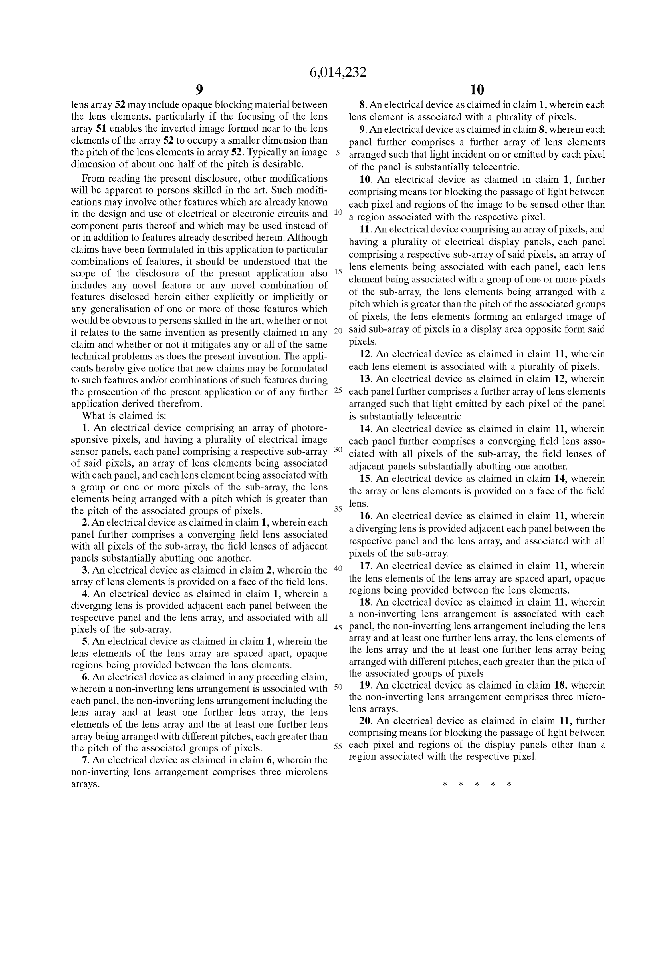
lens array 52 may include opaque blocking material between 8. An electrical device as claimed in claim 1, wherein each the lens elements, particularly if the focusing of the lens lens element is associated with a plurality of pixels. array 51 enables the inverted image formed near to the lens 9. An electrical device as claimed in claim 8, wherein each elements of the array 52 to occupy a Smaller dimension than panel further comprises a further array of lens elements the pitch of the lens elements in array 52. Typically an image arranged Such that light incident on or emitted by each pixel dimension of about one half of the pitch is desirable. of the panel is Substantially telecentric. From reading the present disclosure, other modifications 10. An electrical device as claimed in claim 1, further will be apparent to perSons Skilled in the art. Such modifi comprising means for blocking the passage of light between cations may involve other features which are already known each pixel and regions of the image to be Sensed other than in the design and use of electrical or electronic circuits and a region associated with the respective pixel. component parts thereof and which may be used instead of 11. An electrical device comprising an array of pixels, and or in addition to features already described herein. Although having a plurality of electrical display panels, each panel claims have been formulated in this application to particular comprising a respective Sub-array of Said pixels, an array of combinations of features, it should be understood that the
Scope of the disclosure of the present application also lens 15 elements being associated with each panel, each lens element being associated with a group of one or more pixels includes any novel feature or any novel combination of of the Sub-array, the lens elements being arranged with a features disclosed herein either explicitly or implicitly or pitch which is greater than the pitch of the associated groups any generalisation of one or more of those features which of pixels, the lens elements forming an enlarged image of would be obvious to persons skilled in the art, whether or not it relates to the same invention as presently claimed in any Said Sub-array of pixels in a display area opposite form Said claim and whether or not it mitigates any or all of the same pixels.
technical problems as does the present invention. The appli 12. An electrical device as claimed in claim 11, wherein cants hereby give notice that new claims may be formulated each lens element is associated with a plurality of pixels. to Such features and/or combinations of Such features during 13. An electrical device as claimed in claim 12, wherein the prosecution of the present application or of any further 25 each panel further comprises a further array of lens elements application derived therefrom. arranged Such that light emitted by each pixel of the panel What is claimed is: is Substantially telecentric.
1. An electrical device comprising an array of photore 14. An electrical device as claimed in claim 11, wherein Sponsive pixels, and having a plurality of electrical image each panel further comprises a converging field lens asso Sensor panels, each panel comprising a respective Sub-array ciated with all pixels of the Sub-array, the field lenses of of Said pixels, an array of lens elements being associated adjacent panels Substantially abutting one another. with each panel, and each lens element being associated with 15. An electrical device as claimed in claim 14, wherein a group or one or more pixels of the Sub-array, the lens the array or lens elements is provided on a face of the field elements being arranged with a pitch which is greater than lens.
the pitch of the associated groups of pixels. 35 2. An electrical device as claimed in claim 1, wherein each 16. An electrical device as claimed in claim 11, wherein panel further comprises a converging field lens associated a diverging lens is provided adjacent each panel between the with all pixels of the Sub-array, the field lenses of adjacent respective panel and the lens array, and associated with all pixels of the Sub-array.
panels Substantially abutting one another.
3. An electrical device as claimed in claim 2, wherein the 40 17. An electrical device as claimed in claim 11, wherein array of lens elements is provided on a face of the field lens. the lens elements of the lens array are spaced apart, opaque 4. An electrical device as claimed in claim 1, wherein a regions being provided between the lens elements. diverging lens is provided adjacent each panel between the 18. An electrical device as claimed in claim 11, wherein respective panel and the lens array, and associated with all a non-inverting lens arrangement is associated with each pixels of the Sub-array. 45 panel, the non-inverting lens arrangement including the lens 5. An electrical device as claimed in claim 1, wherein the array and at least one further lens array, the lens elements of lens elements of the lens array are spaced apart, opaque the lens array and the at least one further lens array being regions being provided between the lens elements. arranged with different pitches, each greater than the pitch of 6. An electrical device as claimed in any preceding claim, the associated groups of pixels.
wherein a non-inverting lens arrangement is associated with 50 19. An electrical device as claimed in claim 18, wherein each panel, the non-inverting lens arrangement including the the non-inverting lens arrangement comprises three micro lens array and at least one further lens array, the lens lens arrayS.
20. An electrical device as claimed in claim 11, further elements of the lens array and the at least one further lens comprising array being arranged with different pitches, each greater than means for blocking the passage of light between the pitch of the associated groups of pixels. 55 each pixel and regions of the display panels other than a 7. An electrical device as claimed in claim 6, wherein the region associated with the respective pixel. non-inverting lens arrangement comprises three microlens arrayS.
Provenance
- Collection
- Cited prior art
- Original PDF
- patentimages.storage.googleapis.com →
- Filed
- 1997-09-05
- Pages
- 20
- Method
- pdftotext (the PDF's own text layer) + pdftoppm 300dpi page scans
- Source
- Google Patents bibliographic record
- Granted
- 2000-01-11
- Inventors
- John A. Clarke; US Philips Corp
- Transcribed from
- patentimages.storage.googleapis.com →