patent · US5835514
Laser-based controlled-intensity light source using reflection from a convex surface and method of making same
10 November 1998
Page 1 — bibliographic record
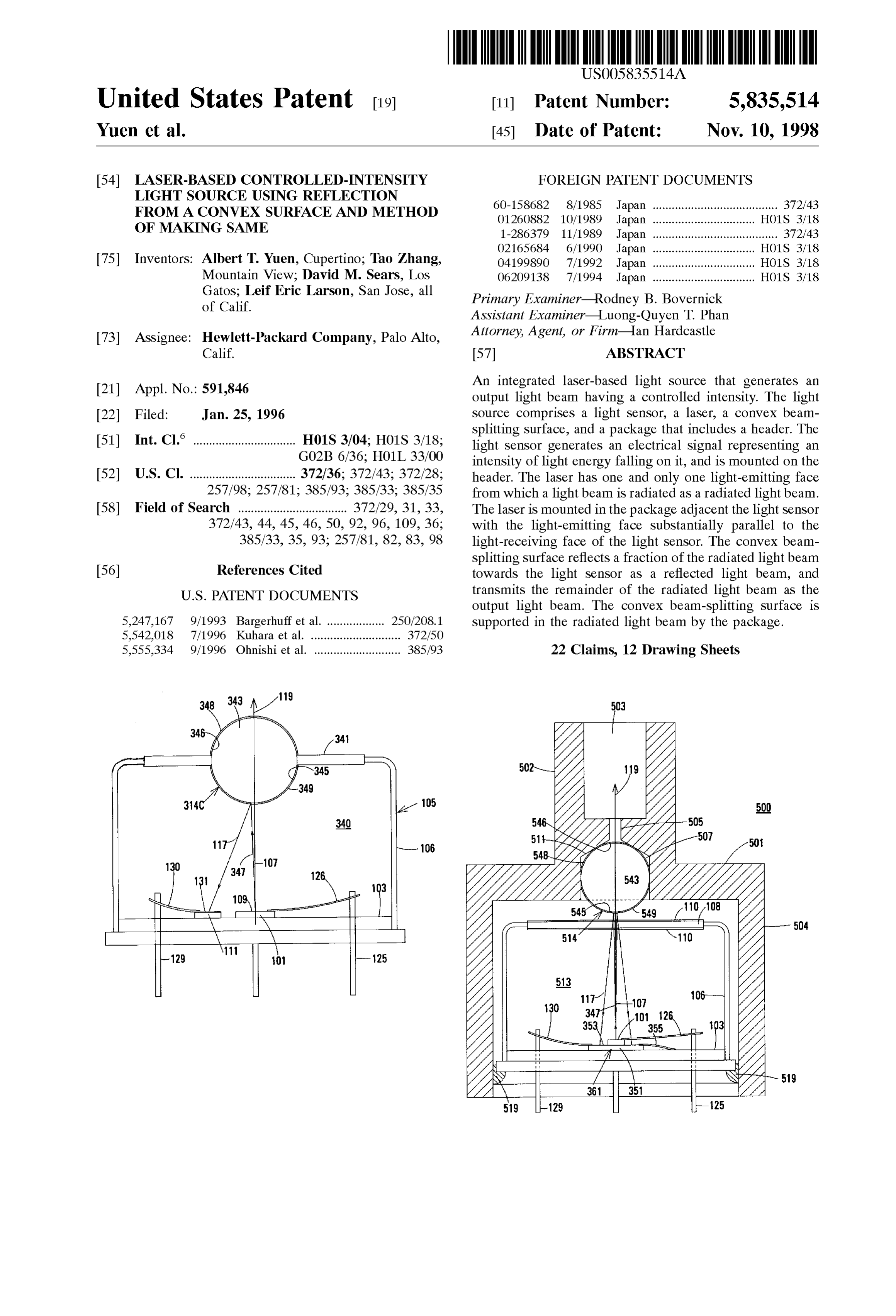
United States Patent (19) 11 Patent Number: 5,835,514 Yuen et al. (45) Date of Patent: Nov. 10, 1998 54) LASER-BASED CONTROLLED-INTENSITY FOREIGN PATENT DOCUMENTS LIGHT SOURCE USING REFLECTION 60-158682 8/1985 Japan ....................................... 372/43
FROM A CONVEX SURFACE AND METHOD
OF MAKING SAME 01260882 10/1989 Japan .
1-286379 11/1989 Japan ....................................... 372/43 02165684 6/1990 Japan . HO1S 3/18 (75) Inventors: Albert T. Yuen, Cupertino; Tao Zhang, O4199890 7/1992 Japan ... HO1S 3/18 Mountain View; David M. Sears, Los 06209138 7/1994 Japan ................................ HO1S 3/18 eif Eric Larson, San Jose, all Primary Examiner Rodney B. Bovernick
Assistant Examiner Luong-Quyen T. Phan 73 Assignee: Hewlett-Packard Company, Palo Alto, Attorney, Agent, or Firm-Ian Hardcastle Calif. 57 ABSTRACT
An integrated laser-based light Source that generates an 21 Appl. No.: 591,846 output light beam having a controlled intensity. The light 22 Filed: Jan. 25, 1996 Source comprises a light Sensor, a laser, a convex beam 6 Splitting Surface, and a package that includes a header. The 51 Int. Cl. ................................ HOS 3/04; HO1S 3/18; light SCSO generates an electrical Signal representing G02B 6/36; H01L 33/00 intensity of light energy falling on it, and is mounted on the 52 U.S. Cl. ................................. 372/36; 372/43; 372/28; header. The laser has one and only one light-emitting face 257/98; 257/81; 385/93; 385/33; 385/35 from which a light beam is radiated as a radiated light beam. 58 Field of Search .................................. 372/29, 31, 33, The laser is mounted in the package ad acent the light SCSO 372/43, 44, 45, 46, 50, 92, 96, 109,36; with the light-emitting face Substantially parallel to the 385/33, 35,93; 257/81, 82, 83, 98 light-receiving face of the light Sensor. The convex beam Splitting Surface reflects a fraction of the radiated light beam 56) References Cited towards the light Sensor as a reflected light beam, and
output light beam. The convex beam-splitting Surface is 5,247,167 9/1993 Bargerhuffet al................... 250/208.1 Supported in the radiated light beam by the package. 5,542,018 7/1996 Kuhara et al. ............................ 372/50 5,555,334 9/1996 Ohnishi et al. ........................... 385/93 22 Claims, 12 Drawing Sheets
Page 2
Drawing sheet — no readable text.
Page 3
Drawing sheet — no readable text.
Page 4
Drawing sheet — no readable text.
Page 5
Drawing sheet — no readable text.
Page 6
Drawing sheet — no readable text.
Page 7
Drawing sheet — no readable text.
Page 8
Drawing sheet — no readable text.
Page 9
Drawing sheet — no readable text.
Page 10
Drawing sheet — no readable text.
Page 11
Drawing sheet — no readable text.
Page 12
Drawing sheet — no readable text.
Page 13
Drawing sheet — no readable text.
Page 14
LASER-BASED CONTROLLED-INTENSITY area will tend to be printed too faintly because of insufficient LIGHT SOURCE USING REFLECTION light output from the laser as a result of the laser temperature FROM A CONVEX SURFACE AND METHOD being too low.
OF MAKING SAME To prevent variations in the light intensity generated by the laser from impairing the performance of the laser printer,
FIELD OF THE INVENTION optical communication link or other laser-based apparatus, it is desirable to employ a control System to vary the laser
This invention relates to laser-based light Sources and, in current to maintain the light intensity at a predetermined particular to laser-based light Sources generating light hav level in the highlight condition or in the low light condition, ing a controlled intensity. or to maintain the light intensity at a first predetermined
BACKGROUND OF THE INVENTION
level in the high light condition and at a Second predeter mined level in the low light condition, irrespective of the
Lasers are used as light Sources in many consumer and temperature and the age of the laser.
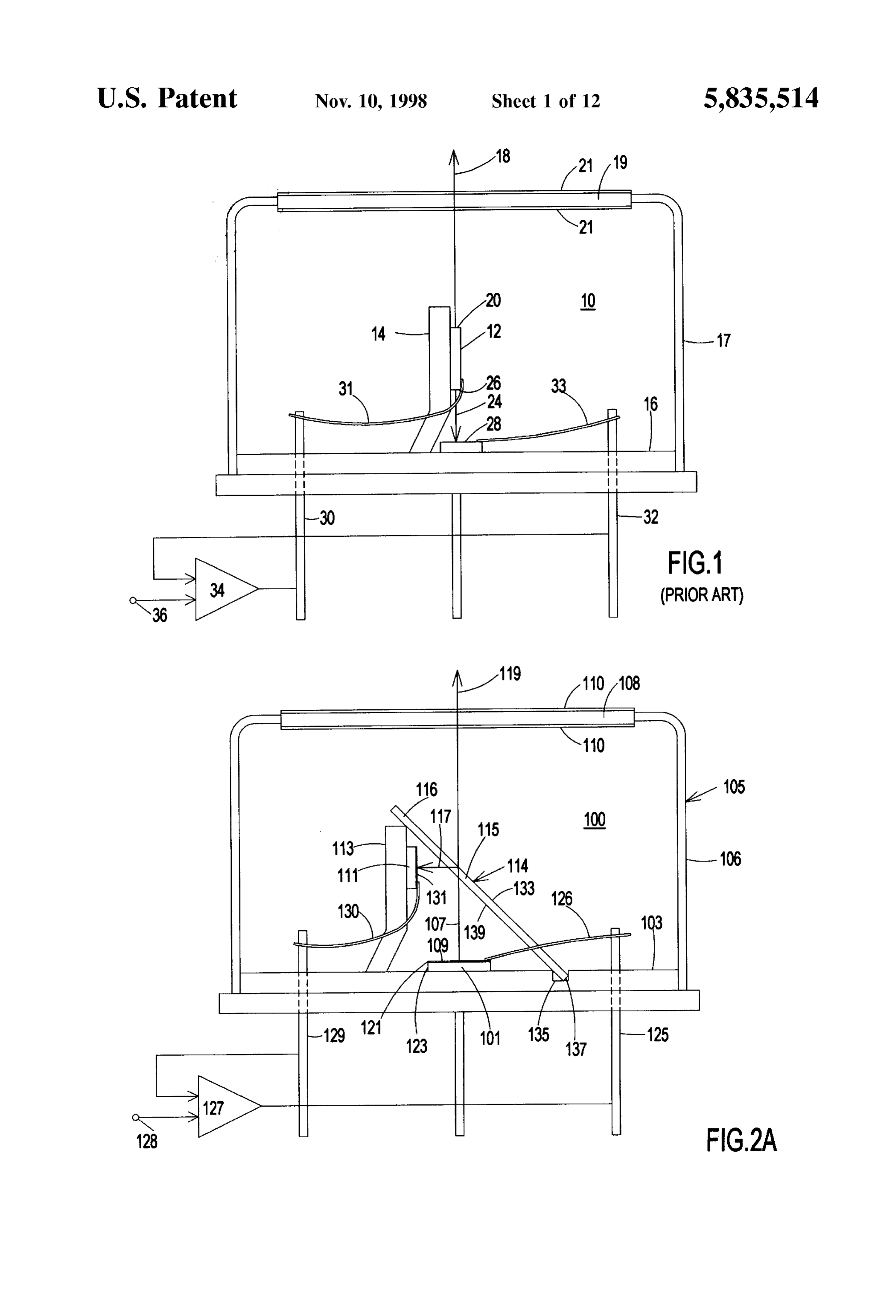
industrial products including laser printers and optical com FIG. 1 shows part of a known laser light source 10 munication linkS. In laser printers, the light output of the 15 generating light with a controlled intensity. In the laser light laser is modulated to Selectively discharge the photo con Source 10, the edge-emitting laser 12 is mounted on the post ductive drum. In optical communication links, the light 14 projecting from the header 16. The can 17 is attached to output of the laser is modulated to represent the States of a the header 16, and usually forms a hermetic seal with the digital information signal. LaserS having a modulated light header. The can includes the window 19 though which the output are also used to write a digital information Signal on light beam 18 generated by the laser 12 is emitted. The an optical disc, for example. In these and other applications, window is normally coated with the anti-reflective layer 21 the need to modulate the light output of the laser at high to prevent the window from reflecting part of the light beam Speed normally precludes modulating the light output by 18 back into the laser 12.
Simply Switching the laser on and off. Instead, the light The edge-emitting laser 12 is formed by creating a output of the laser is modulated between a high light 25 Structure in a Suitable Semiconductor Such as gallium arS condition and a low light condition, which is normally just enide. The edge-emitting laser 12 emits the light beam 18 in above threshold level of the laser. However, in the following response to a current Supplied from an external power Source disclosure, the low-light condition will be regarded as via the conductor 30, which passes through an electrically encompassing the Zero-light condition in which the laser isolated passage (not shown) in the header 16, and the current is reduced to below the threshold current or to zero. bonding wire 31, which connects the conductor 30 to a When the light output of the laser is modulated between metallization layer (not shown) on the laser 12. The edge a high light condition and a low light condition, the light emitting laser 12 emits the light beam 18 from a very narrow intensity in at least one of the two light conditions must be aperture about 0.1 um wide in the cleaved edge 20, and also well defined. For example, in the laser printer application, emits the Secondary light beam 24 from the cleaved edge 26, when the low light condition is above the Zero light 35 opposite the cleaved edge 20.
condition, the light intensity in the low light condition must In applications in which the intensity of the light gener remain below the discharge threshold of the photo conduc ated by the edge-emitting laser 12 must be controlled, the tive drum. Moreover, since the size of the spot on the photo light sensor 28 is mounted on the header 16 positioned to be conductive drum discharged by the light beam depends on directly illuminated by the secondary light beam 24. The the intensity of the light beam, the intensity of the laser in 40 light Sensor 28 is typically a Silicon, gallium arsenide, or the high light condition must also be defined to ensure indium gallium arsenide photo diode, the type depending on consistent line widths. In the optical communication link the wavelength of the light generated by the laser 12. The application, the difference between the high light condition electrical output of the light sensor 28 is fed to the outside and the low light condition may be made relatively Small to of the package by the conductor 32, which passes through an maximize the modulation rate, and hence the data transmis 45 electrically-isolated passage (not shown) in the header, and Sion Speed. The light intensities in both light conditions must the bonding wire 33, which connects the conductor 32 to a be accurately defined to enable the two light conditions to be metallization layer (not shown) on the light sensor 28. distinguished from one another by the receiver of the optical The conductor 32 is also connected to the control circuit communication link. 34. The control circuit also receives a digital input signal via The light intensity generated by a Semiconductor laser for 50 the input terminal 36. The State of the digital input Signal a given laser current depends primarily on the temperature determines whether the control circuit drives the laser 12 to of the laser. Aging is a Secondary factor. The temperature of emit the light beam in the high light condition or in the low the laser depends in part on the magnitude and the duty cycle light condition. The control circuit 34 controls the current of the current through the laser, i.e., the laser current. The fed to the laser 12 via the conductors 30 and 31 to obtain a duty cycle of the laser depends on the digital input Signal 55 predetermined value of the electrical output of the light modulating the laser. For example, in a laser printer, the laser sensor 28 in one or both of the high light condition and the continuously generates light in the high light condition to low light condition. This predetermined value of the output create “area fills,” and continuously generates light in the of the light Sensor 28 corresponds to the Secondary light low light condition to create white areas, Such as margins beam 24 having a predetermined intensity in the respective and borders. The thermal time constant of a typical Semi 60 light condition. Since the intensity of the Secondary light conductor laser is very rapid, of the same order as the time beam 24 has a substantially linear relationship to that of the required to print about ten pixels. Thus, if the light output of primary light beam 18, the light sensor 28 monitoring the the laser increases with increasing temperature, for example, intensity of the Secondary light beam 24 conveniently pro the temperature, and hence the light output, of the laser will vides an acceptably accurate control of the intensity of the Steadily increase (with a resulting increase in print density 65 primary light beam 18.
and line width) in the course of printing an area fill. On the Recently, Vertical-cavity Surface-emitting lasers other hand, isolated narrow vertical lines printed in a white (VCSELs) have been introduced. Such lasers are formed in
Page 15
a structure of Semiconductor layerS deposited on a Semicon Signal representing the intensity of light energy falling on it, ductor Substrate, and emit light from a port in the Surface of and is mounted on the header. The laser has one and only one the Structure, instead of from the very narrow region about light-emitting face from which a light beam is radiated as a 0.1 um wide on the cleaved edge of the device, as in an radiated light beam. The laser is mounted in the package edge-emitting laser. AVCSEL offers numerous performance adjacent the light Sensor with the light-emitting face Sub advantages over an edge-emitting laser. For example, a Stantially parallel to the light-receiving face of the light VCSEL inherently has a smaller numeric aperture and Sensor. The convex beam-splitting Surface reflects a fraction generates a much more Symmetrical light beam than an of the radiated light beam towards the light Sensor as a edge-emitting laser. As a result, the light from the VCSEL reflected light beam, and transmits the remainder of the can be coupled into the optical System of the laser printer or radiated light beam as the output light beam. The convex optical communication link more efficiently than the light beam-splitting Surface is Supported in the radiated light from the edge-emitting laser. The increased coupling effi beam by the package.
ciency enables the VCSEL to be run at lower power to The convex beam-splitting Surface reflects the fraction of produce a given light intensity. However, the VCSEL gen the radiated light beam towards the light Sensor while erally emits a Single light beam instead of the two light 15 minimizing the intensity of light returning to the laser beams emitted by the edge-emitting laser. Therefore, a following reflection by the light Sensor and a Second reflec VCSEL-based light Source generating light with a controlled tion by the convex beam-splitting Surface. The reflected light intensity cannot be made simply by substituting the VCSEL beam diverges from the convex beam-splitting Surface, for the edge-emitting laser 12 in the arrangement shown in which reduces the accuracy with which the light Sensor must FIG.1. An alternative arrangement is required to monitor the be located relative to the laser to receive the reflected light intensity of the light generated by the VCSEL. beam.
A possible solution for this problem is described in G. The convex beam-splitting Surface may include a reflec Hasnian et al., Monolithic Integration of Photodiode with tion control element that determines the intensity ratio Vertical Cavity Surface Emitting Laser, 27 ELECTRONICs between the reflected light beam and the output light beam. LETTERS 18, p. 1630 (1991). In this, a p-i-n photo diode is 25 The laser and the light Sensor may be mounted Side-by grown on the p-type mirror region of a top-emitting VCSEL.
Although this arrangement gives a good monitoring Side on on the header. Alternatively, the laser may be mounted part of the light-receiving face of the light Sensor.
performance, it increases the complexity of the manufactur
The ing process because additional epitaxial layerS must be the can may Support package may include a can attached to the header, and deposited to provide the layers of the photo diode, and the convex beam-splitting Surface in the because an additional etching process is required to delin radiated light beam.
eate the photo diode. Moreover, the etching process leaves The light Source may additionally comprise a lens that the edges of the layers exposed to contamination which can includes the convex beam-splitting Surface. compromise the reliability and accuracy of the arrangement. The package may include an axial bore in which the lens U.S. Pat. No. 5,491,712, assigned to the Assignee of the 35 is mounted, and a body portion optically aligned with the present application, describes Some alternative arrange axial bore. In this embodiment, the body portion is dimen ments for monitoring the intensity of the light generated by Sioned to accommodate the header in an adjustable position a VCSEL. In a first one of these, a Schottky structure is relative to the lens, and the axial bore includes a portion formed as a photo detector on the top Surface of the layer 40 dimensioned to receive an optical fibre and to position the structure in which the VCSEL is formed. This arrangement optical fibre accurately in a predetermined position relative also requires that additional layers be deposited on the layer to the lens.
structure of the VCSEL, albeit fewer than the number of The laser, the light Sensor and the convex beam-splitting additional layerS required for the p-i-n photo diode. Surface may be arranged Such that light reflected by the In a Second arrangement, a photo detector is delineated 45 light-receiving face of the light Sensor is directed away from adjacent the VCSEL in the layer structure in which the the light-emitting face of the laser to reduce noise in the VCSEL is formed. Light is transmitted laterally in the layer output light beam.
structure between the light-generating layer of the VCSEL The light Source may additionally include a controller that and the photo detector. The magnitude of the current flowing controls the laser current in response to the electrical Signal through the photo detector in response to a reverse bias 50 generated by the light Sensor. The controller may addition applied to the photo detector (as opposed to the forward bias ally control the laser current to limit the electrical Signal to which the VCSEL is subject) represents the intensity of generated by the light Sensor to a predetermined maximum the light in the light generating layer of the VCSEL. This corresponding to a predetermined maximum intensity of the arrangement provides a structurally-Simple way to monitor output light beam.
the intensity of the light in the light-generating layer of the 55 The radiated light beam generated by the laser may have VCSEL, but may not provide an acceptable intensity moni a Signal-to-noise ratio that depends on its intensity. The toring accuracy because the relationship between the inten intensity at which the radiated light beam has a signal-to sity of the light in the light-generating layer and the intensity noise ratio above a threshold level may be greater than a of the light beam actually emitted by the VCSEL is not well predetermined maximum intensity. In this case, the beam defined. 60 Splitting Surface may reflect Such a fraction of the radiated
SUMMARY OF THE INVENTION
light beam to the light Sensor that the output light beam has a signal-to-noise ratio greater than the threshold level and an
The invention provides an integrated laser-based light intensity less than the predetermined maximum intensity. Source that generates an output light beam having a con The invention also provides an integrated laser-based trolled intensity. The light Source comprises a light Sensor, a 65 light Source for illuminating an optical fibre with an output laser, a convex beam-splitting Surface, and a package that light beam having a controlled intensity. The light Source includes a header. The light Sensor generates an electrical comprises a laser/sensor assembly, a ball lens, and a pack
Page 16
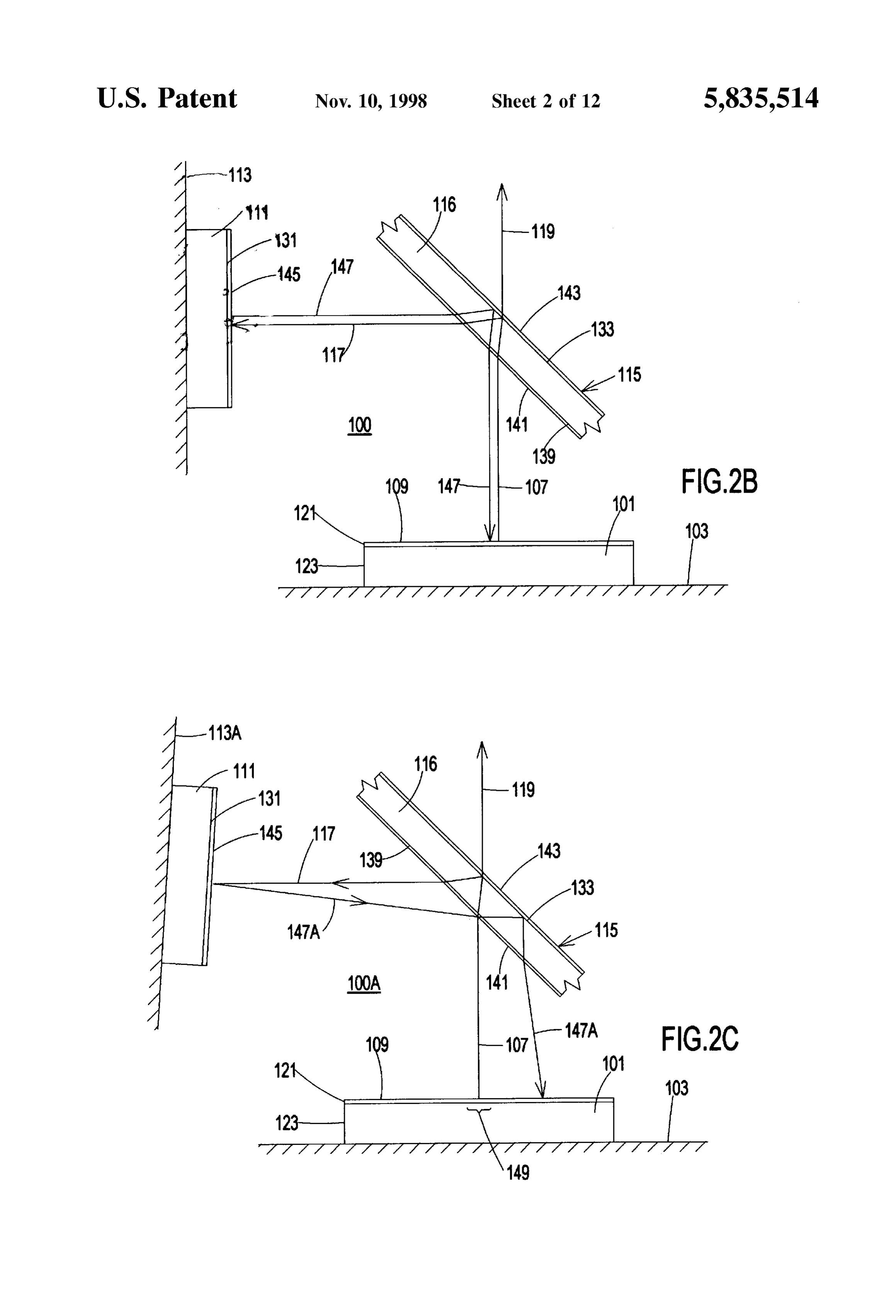
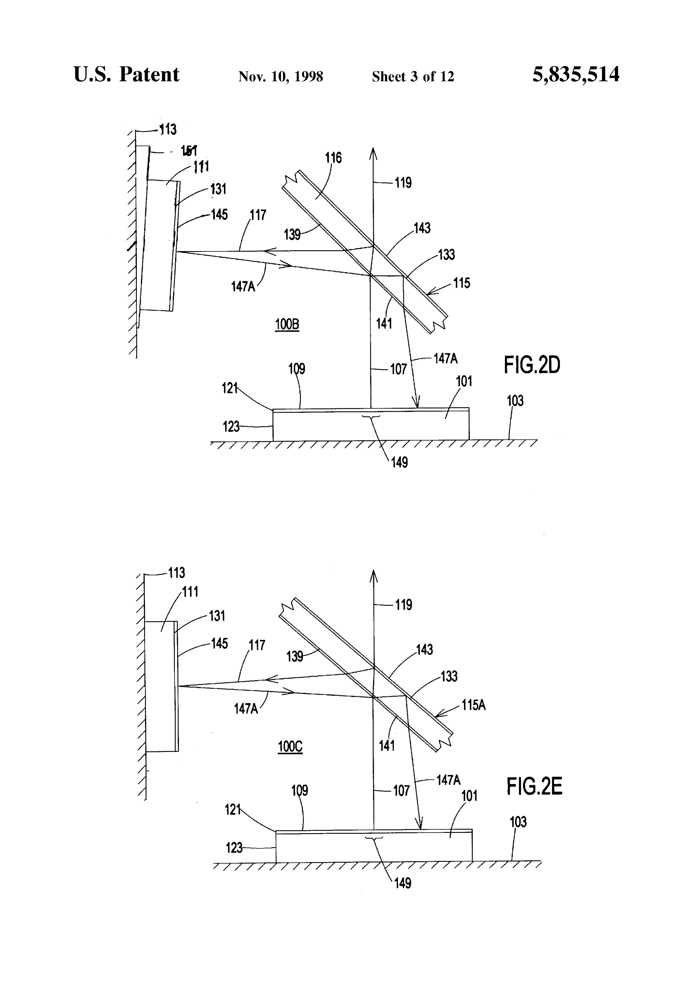
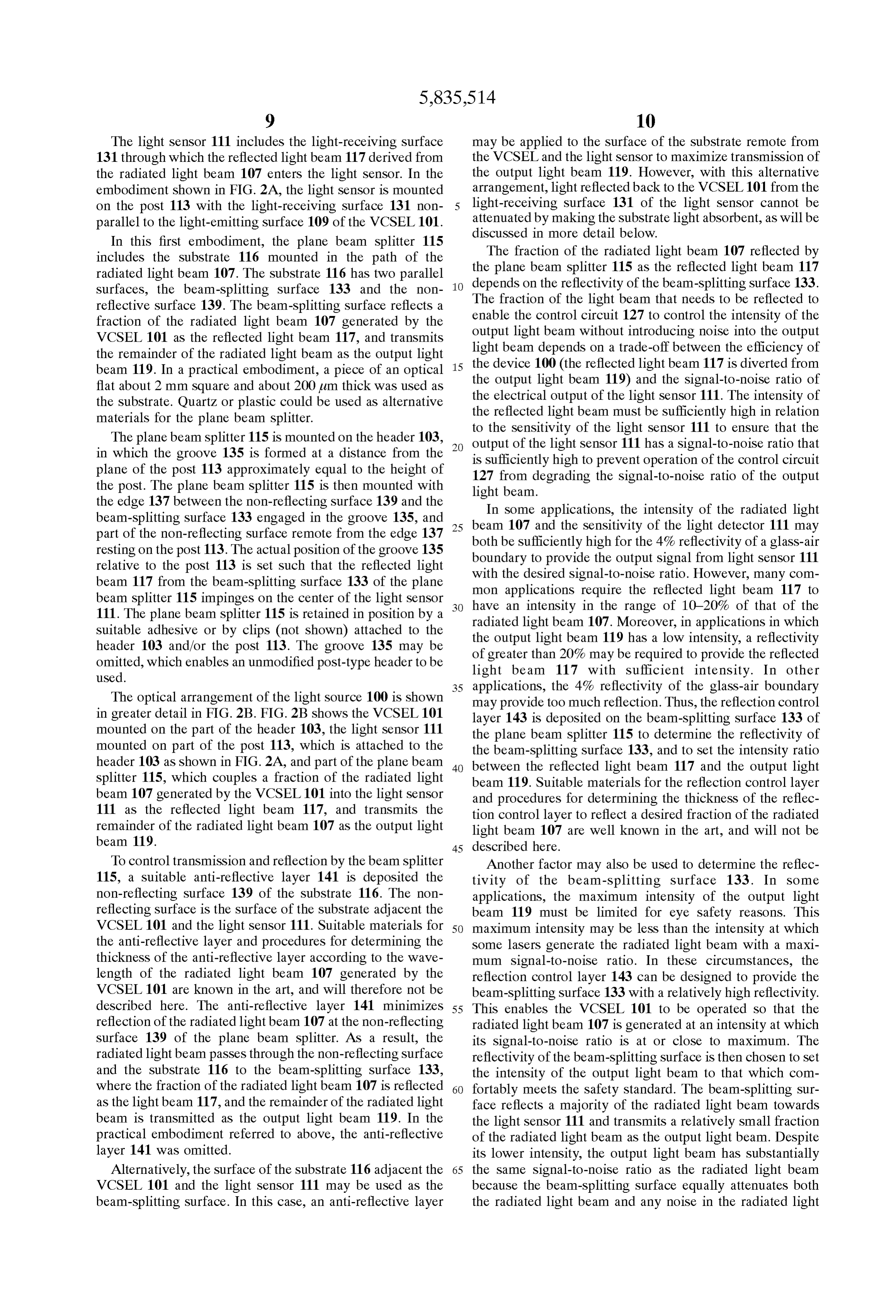
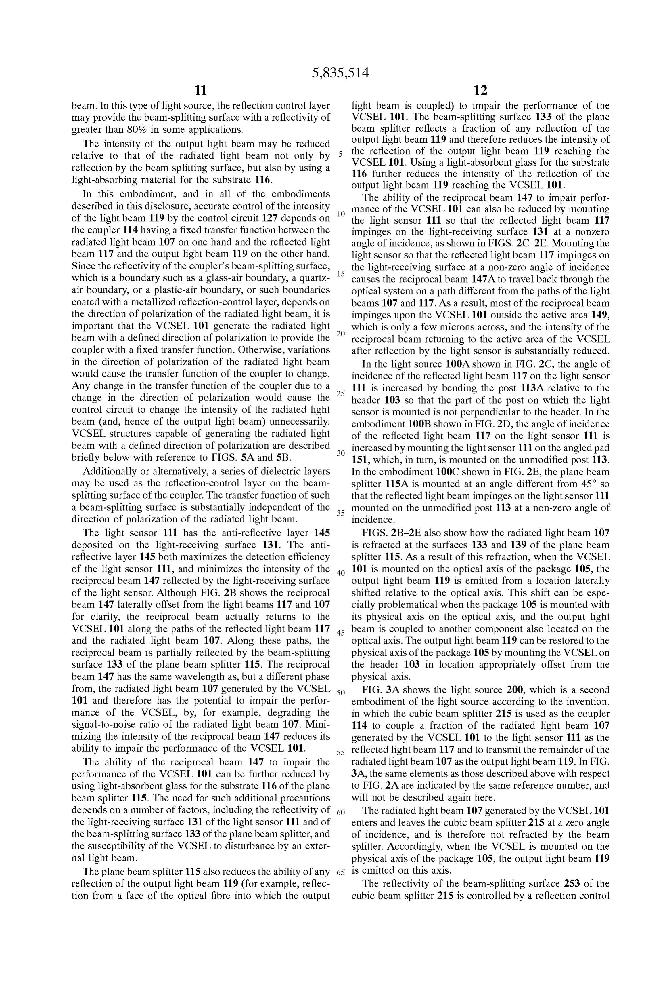
S 6 age. The laser/sensor assembly includes a header, a light FIGS. 2C-2E show three alternative structures for attenu Sensor, and a laser. The light Sensor generates an electrical ating the light re-entering the laser following reflection of Signal representing the intensity of light energy falling on it, the reflected light beam by the light sensor in the embodi and is mounted on the header. The laser has one and only one ment of the integrated laser-based light Source according to light-emitting face from which a light beam is radiated as a the invention shown in FIG. 2A.
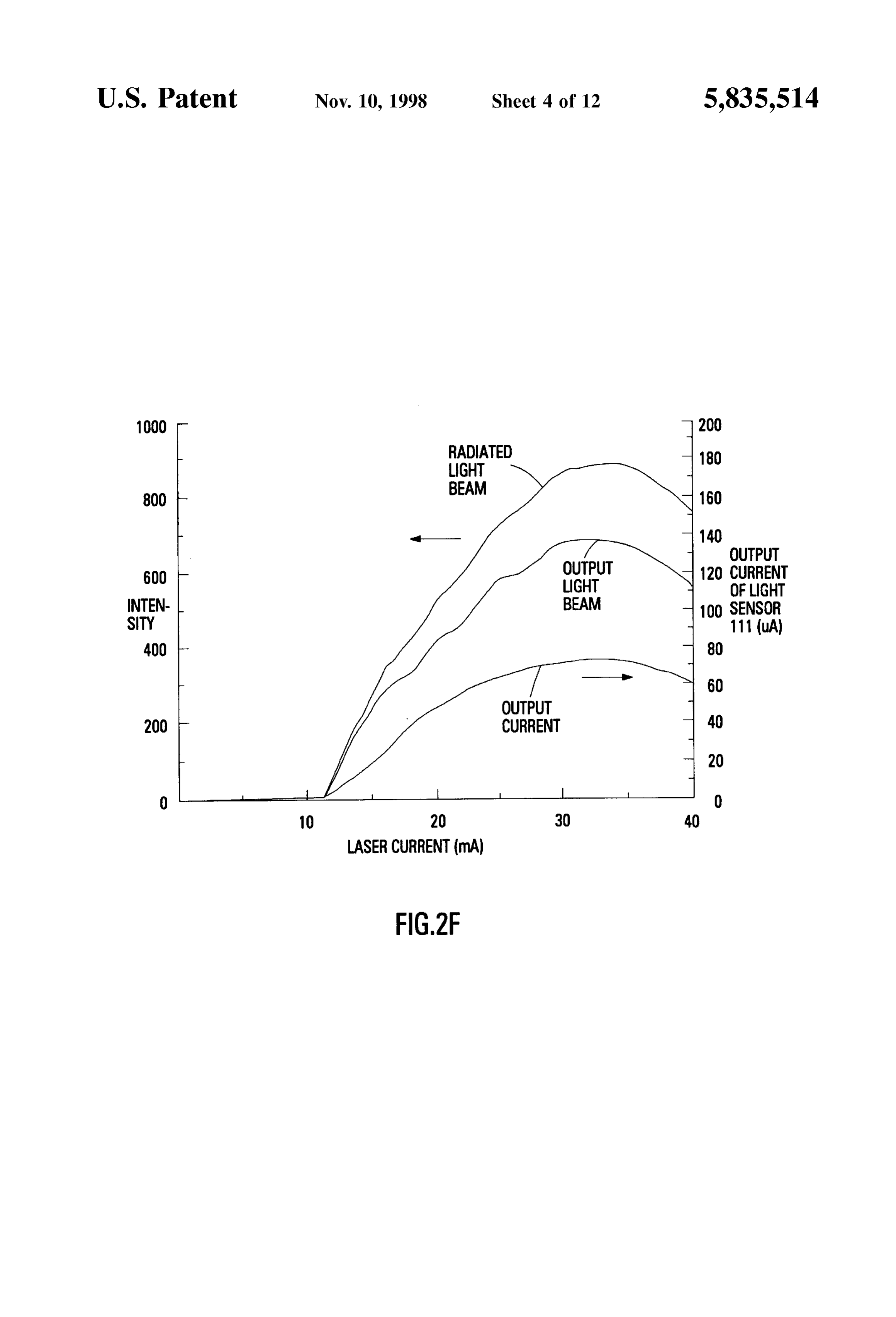
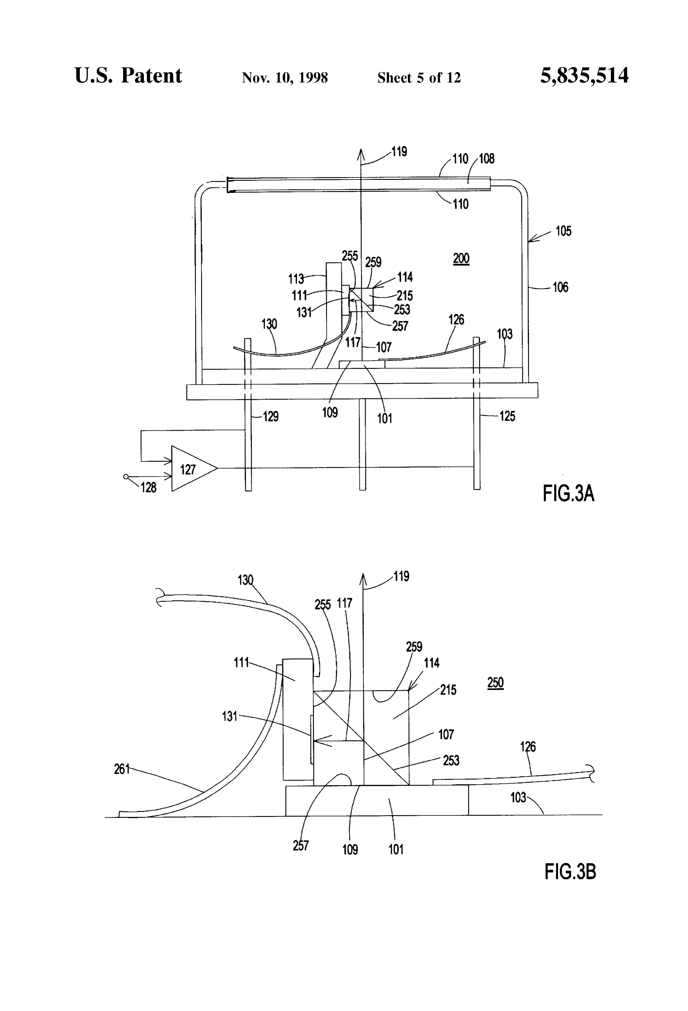
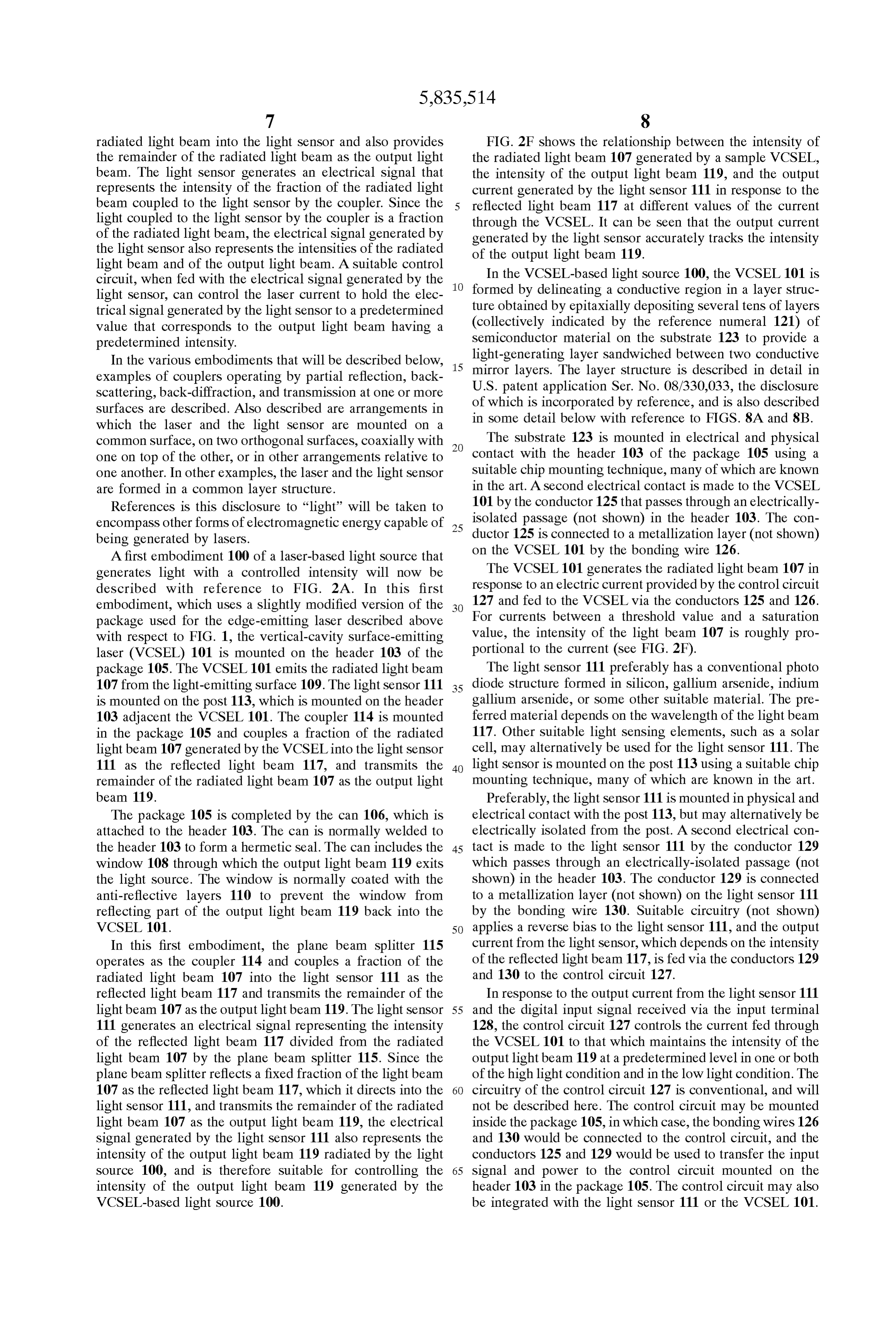
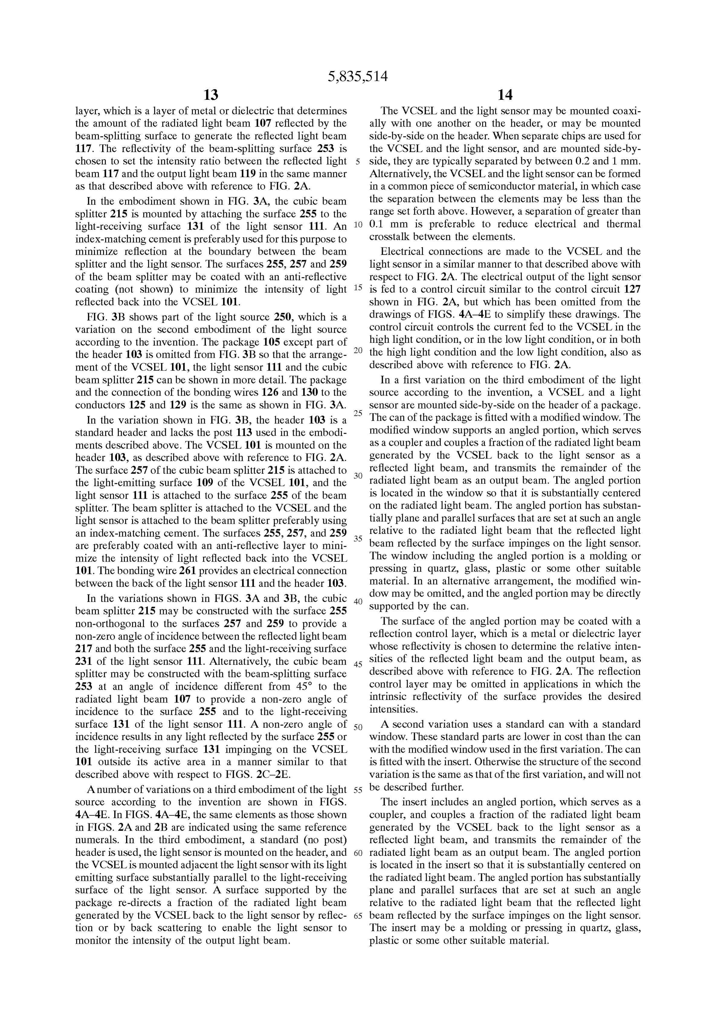
radiated light beam. The laser is mounted adjacent the light FIG. 2F is a graph showing the relationship between the Sensor with the light-emitting face Substantially parallel to intensity of the light beam generated by a sample VCSEL, the light-receiving face. The package includes an axial bore the intensity of the output light beam, and the output current and a body portion. The ball lens is mounted in the axial generated by the light Sensor in response to the reflected bore, which includes a portion dimensioned to receive the light beam at different values of the current through the optical fibre and to position the optical fibre accurately relative to the ball lens. The body portion is optically aligned VCSEL in the embodiment of the integrated laser-based with the axial bore and is dimensioned to adjustably accom light Source according to the invention shown in FIG. 2A. modate the laser/Sensor assembly in a position, relative to FIG.3A shows a side view of a second embodiment of the the ball lens, at which the ball lens reflects a fraction of the 15 integrated laser-based light Source according to the inven radiated light beam towards the light Sensor as a reflected tion.
light beam, at which the ball lens transmits a remainder of FIG. 3B shows details of a variation on the embodiment the radiated light beam as the output light beam, and at of the integrated laser-based light Source according to the which the intensity of the output light beam is maximized. invention shown in FIG. 3A.
The laser and the light Sensor may be mounted Side-by FIG. 4A shows a side view of a third variation on a third Side on the header. Alternatively, the laser may be mounted embodiment of the integrated laser-based light Source on part of the light-receiving face of the light Sensor. according to the invention.
Finally, the invention provides a method of making an FIG. 4B shows a side view of a fourth variation on the integrated laser-based light Source for illuminating an opti third embodiment of the integrated laser-based light Source cal fibre with an output light beam having a controlled 25 according to the invention.
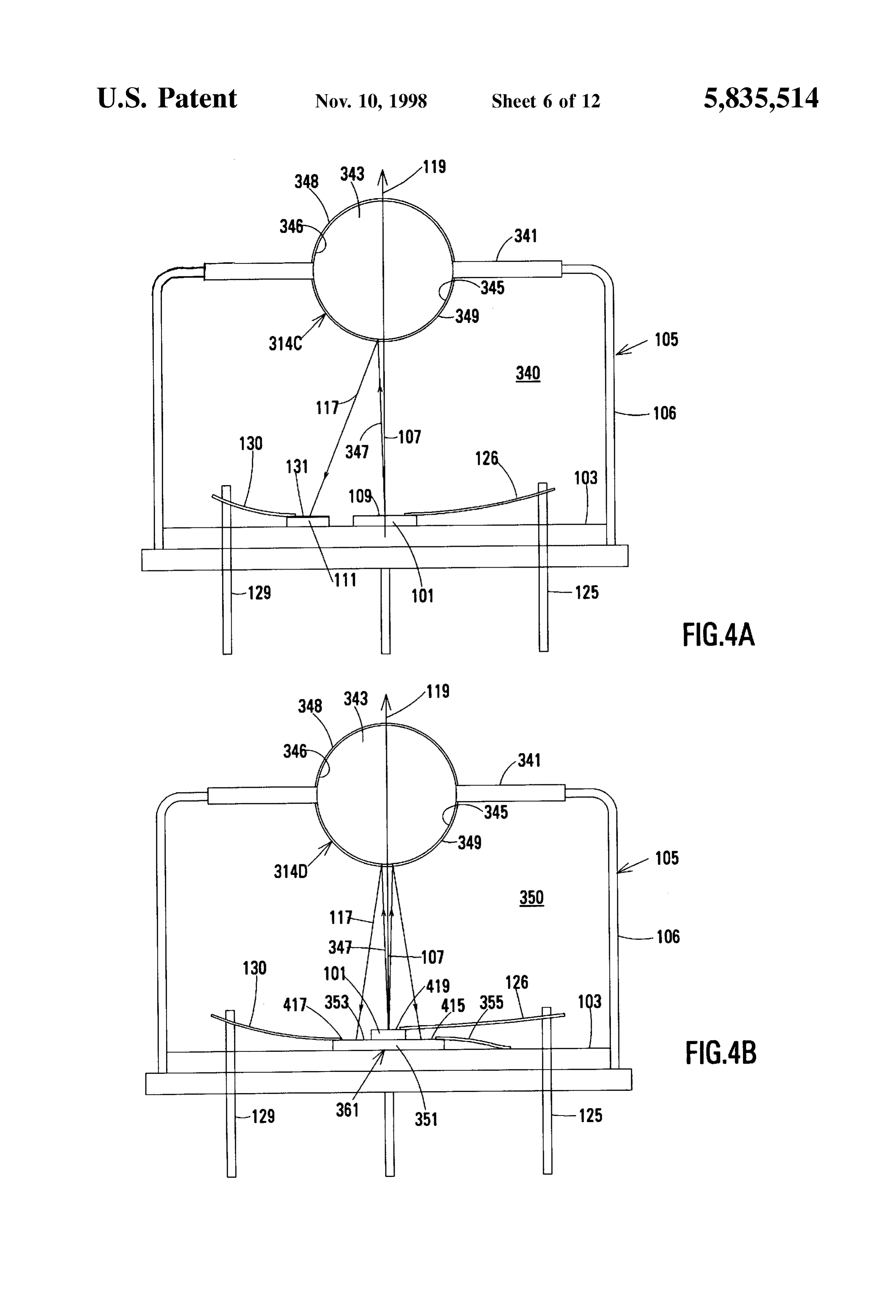
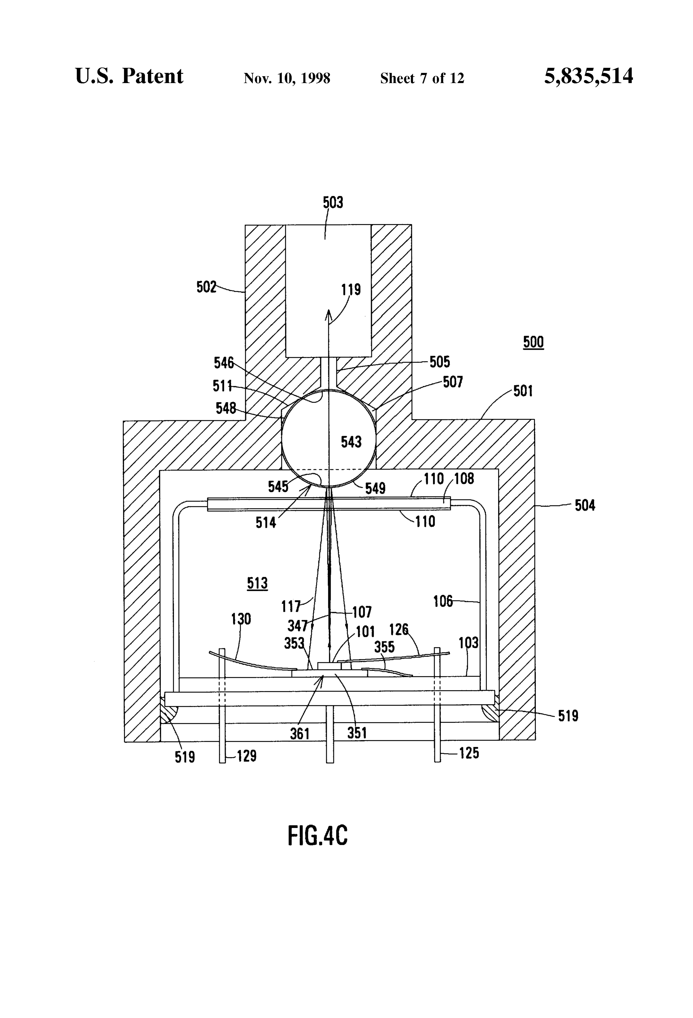
intensity. In the method, a laser/sensor assembly, a lens FIG. 4C shows a cross-sectional view of a fifth variation having a conveX Surface, and a package are provided. The on the third embodiment of the integrated laser-based light laser/sensor assembly includes a header, a light Sensor, and Source according to the invention.
a laser. The light Sensor generates an electrical signal FIG. 4D shows a side view of a sixth variation of a third representing the intensity of light energy falling on it, and is embodiment mounted on the header. The laser has one and only one according to the of the integrated laser-based light Source light-emitting face from which a light beam is radiated as a invention.
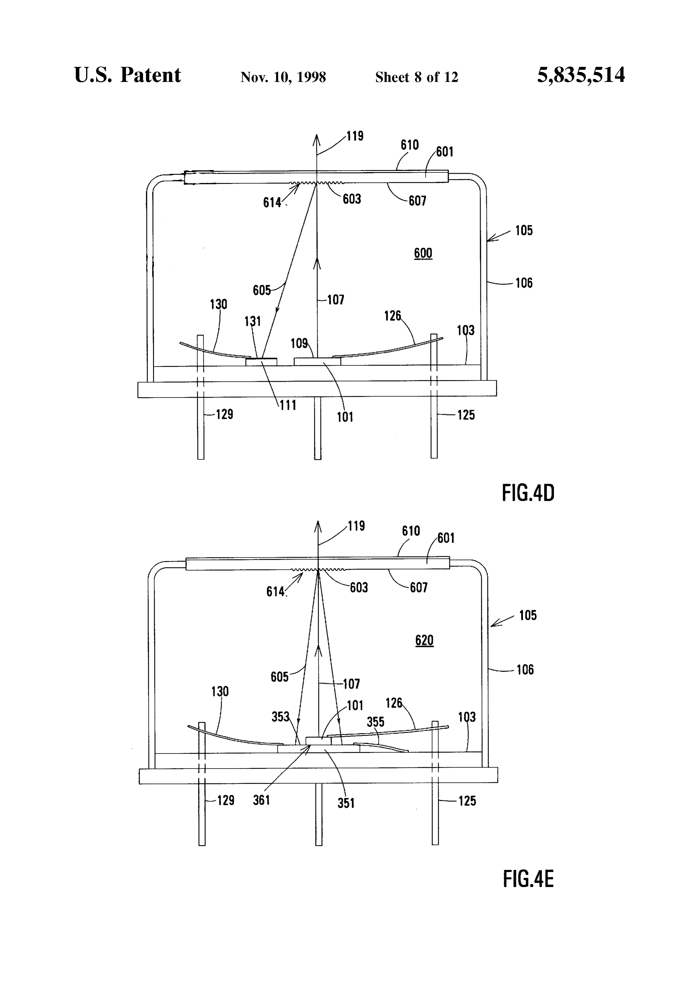
radiated light beam, and is mounted adjacent the light Sensor FIG. 4E shows a side view of a seventh variation of the with the light-emitting face Substantially parallel to the third embodiment of the integrated laser-based light Source light-receiving face. The package includes an axial bore 35 according to the invention.
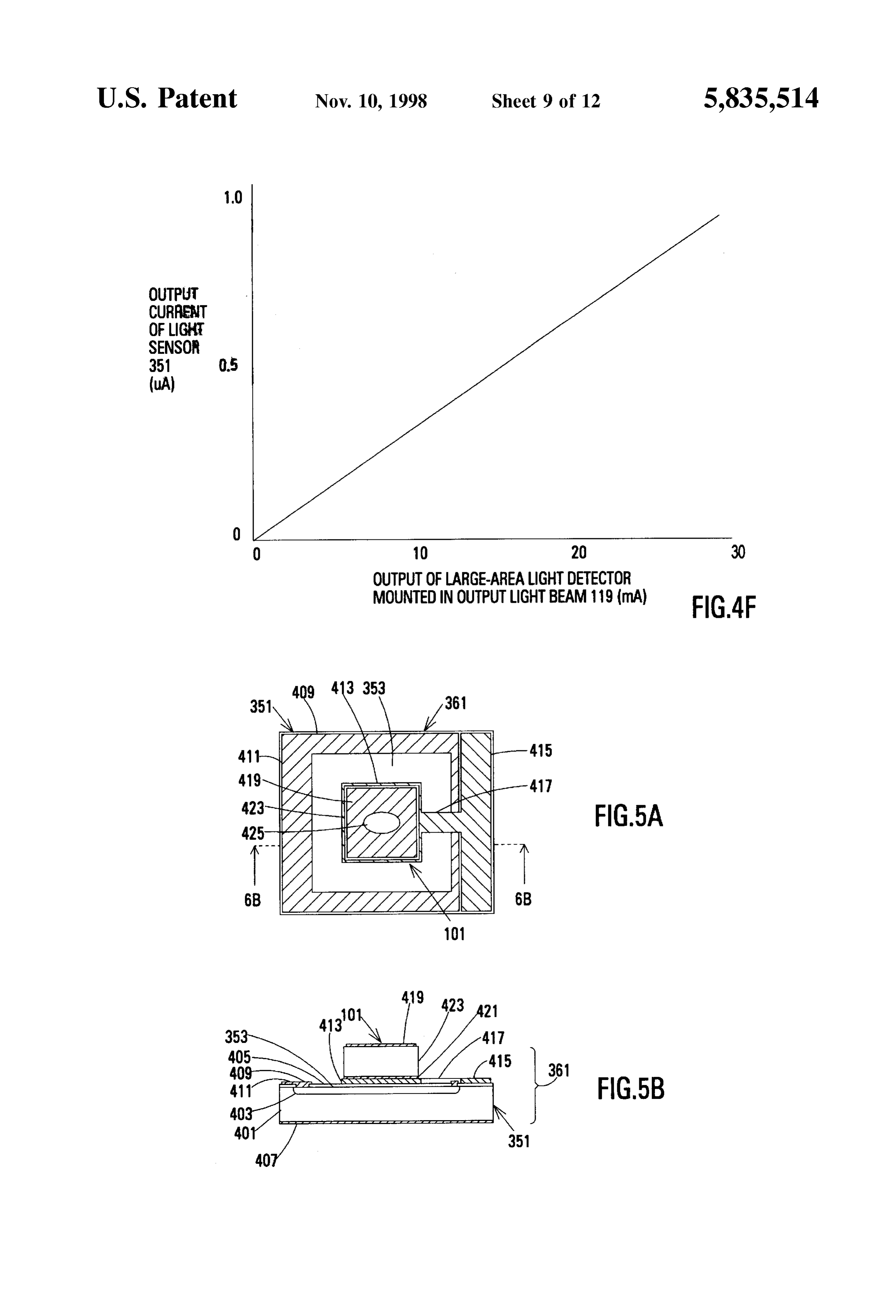
including portions dimensioned to receive the lens and the FIG. 4F is a graph showing the output current of the light optical fibre Such that the optical fibre is positioned accu detector plotted against the output of a large-area light rately in a predetermined position relative to the lens. The detector mounted in the output light beam generated by the package also includes a body portion optically aligned with variation shown in FIG. 4B.
the axial bore and dimensioned to receive the laser/Sensor 40 FIGS.5A and 5B respectively show a top view and a cross assembly with a clearance fit. sectional view of the VCSEL/light sensor assembly used in The lens is mounted in the axial bore of the package. The the variations shown in FIGS. 4B, 4C and 4E. laser/sensor assembly is inserted into the body portion to a FIG. 6A shows a side view of a fourth embodiment of the position at which the conveX Surface of the lens reflects a integrated laser-based light Source according to the inven fraction of the radiated light beam towards the light Sensor 45 tion.
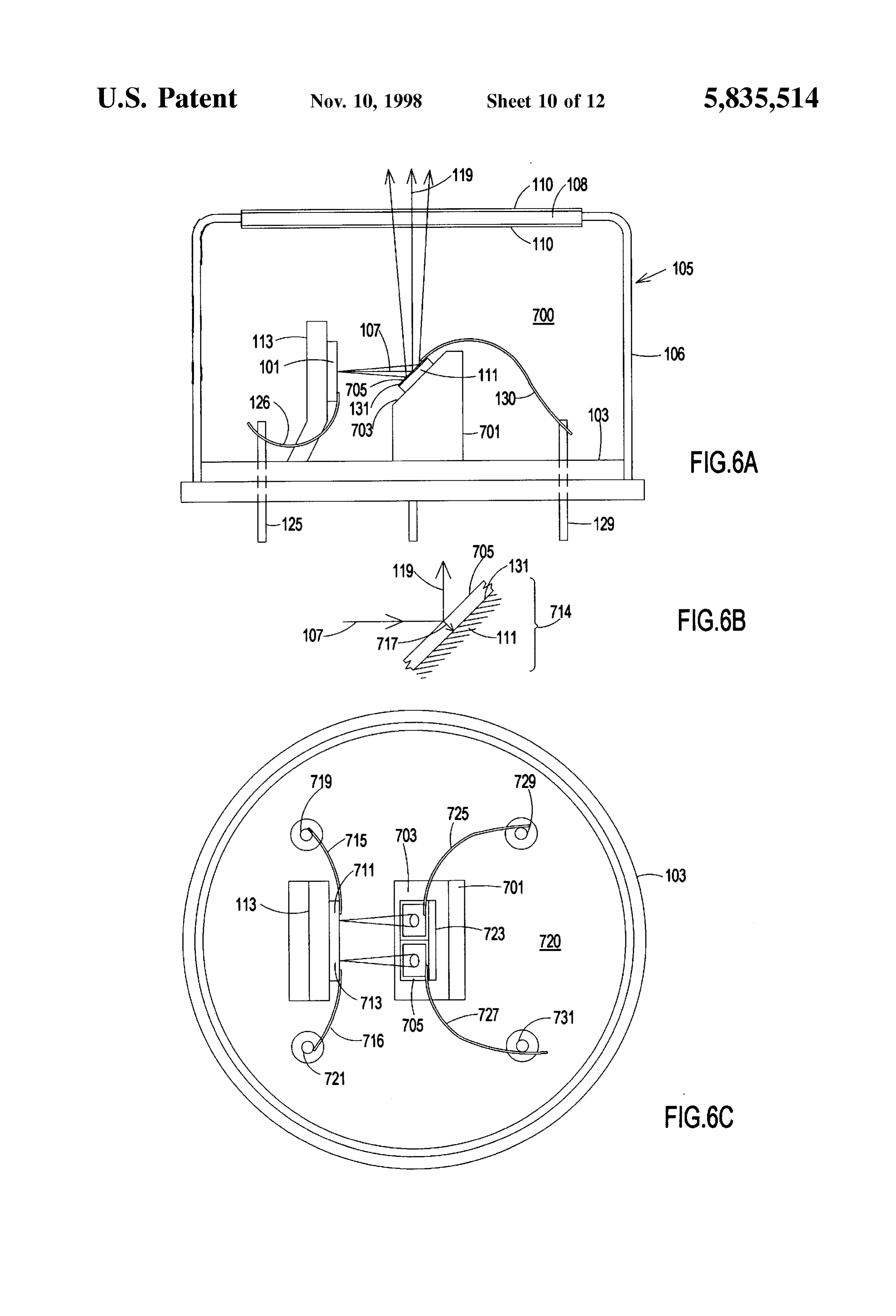
as a reflected light beam, and the lens transmits a remainder FIG. 6B shows details of the optical arrangement of the of the radiated light beam as the output light beam. The fourth embodiment of the integrated laser-based light Source position of the laser/Sensor assembly relative to the lens is according to the invention.
adjusted to maximize the intensity of the output light beam.
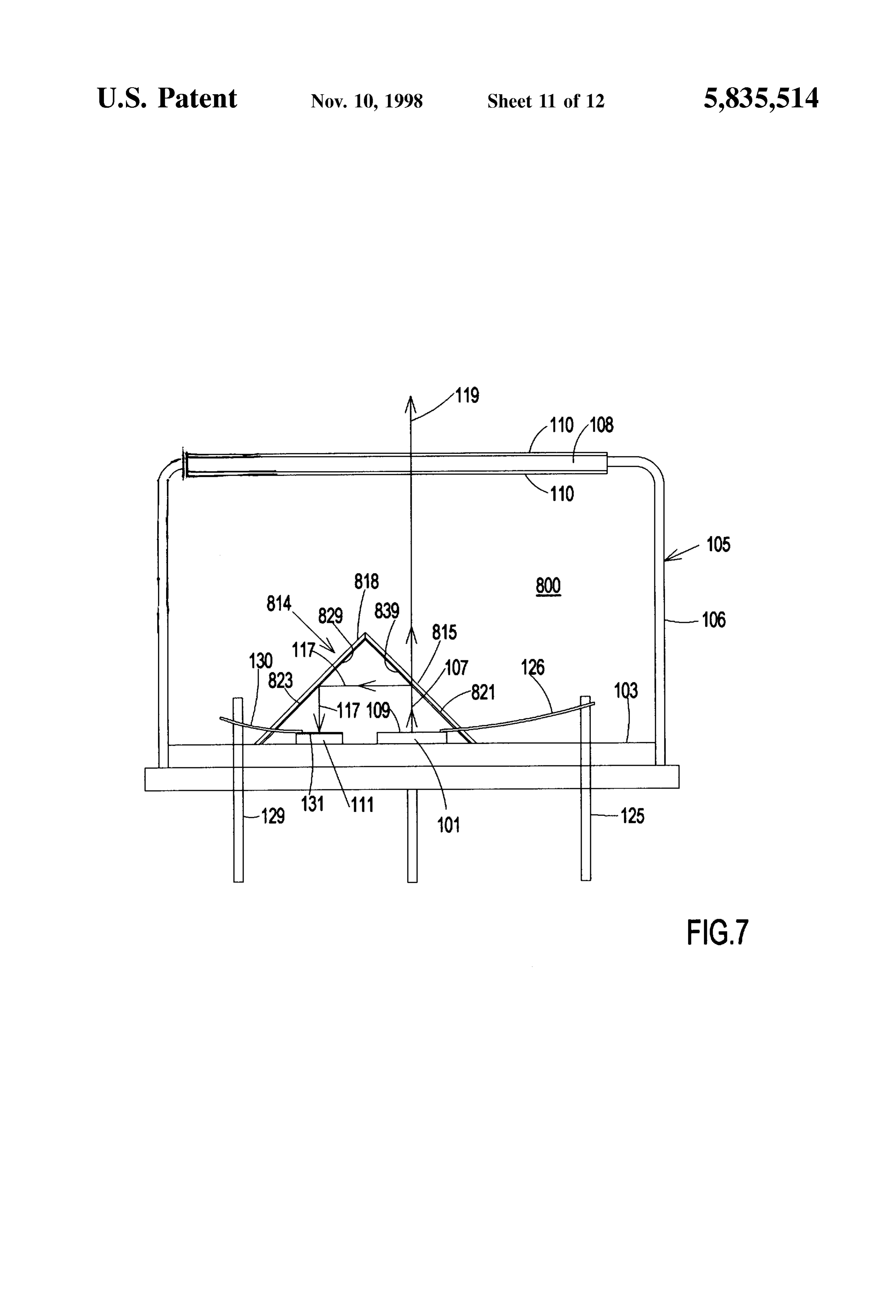
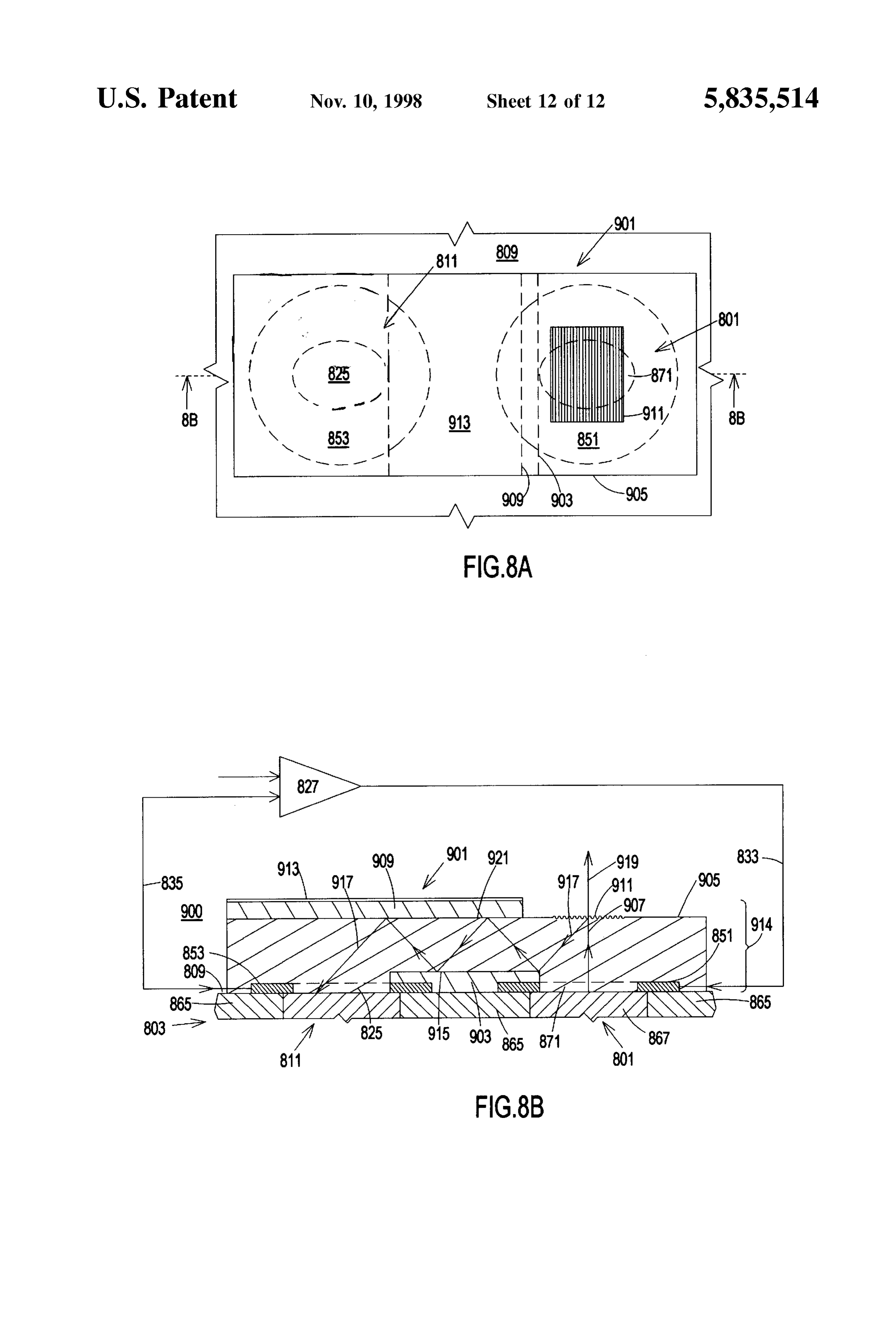
Finally, the laser/sensor assembly is fixed in the body 50 FIG. 6C shows a top view of the fourth embodiment of the portion at the position at which the intensity of the output integrated laser-based light Source according to the inven light beam is a maximum. tion adapted to operate with an array of lasers. A curable adhesive may be applied to at least one of the FIG. 7 is a side view of a fifth embodiment of the body portion and the laser/Sensor assembly, and the adhesive tion. integrated laser-based light Source according to the inven may be cured to fix the laser/sensor assembly in the body 55 portion. FIGS. 8A and 8B respectively show a top view and a BRIEF DESCRIPTION OF THE DRAWINGS croSS-Sectional view of a sixth embodiment of the integrated laser-based light Source according to the invention.
FIG. 1 shows a side view of a known integrated light
Source generating light with a controlled intensity based on 60 DETAILED DESCRIPTION OF THE an edge-emitting laser. INVENTION FIG. 2A shows a side view of a first embodiment of an An integrated laser-based light Source according to the integrated laser-based light Source according to the inven invention has a laser and a light Sensor mounted in a tion for generating light with a controlled intensity. common package. The laser generates a radiated light beam FIG. 2B shows more details of the optical arrangement of 65 in response to a laser current. A coupler is also mounted in the embodiment of the integrated laser-based light Source the package in a position Such that it is illuminated by the according to the invention shown in FIG. 2A. radiated light beam. The coupler couples a fraction of the
Page 17
radiated light beam into the light Sensor and also provides FIG. 2F shows the relationship between the intensity of the remainder of the radiated light beam as the output light the radiated light beam 107 generated by a sample VCSEL, beam. The light Sensor generates an electrical Signal that the intensity of the output light beam 119, and the output represents the intensity of the fraction of the radiated light current generated by the light Sensor 111 in response to the beam coupled to the light Sensor by the coupler. Since the reflected light beam 117 at different values of the current light coupled to the light Sensor by the coupler is a fraction through the VCSEL. It can be seen that the output current of the radiated light beam, the electrical Signal generated by generated by the light Sensor accurately tracks the intensity the light Sensor also represents the intensities of the radiated of the output light beam 119.
light beam and of the output light beam. A Suitable control circuit, when fed with the electrical Signal generated by the In the VCSEL-based light source 100, the VCSEL 101 is light Sensor, can control the laser current to hold the elec formed by delineating a conductive region in a layer Struc trical Signal generated by the light Sensor to a predetermined ture obtained by epitaxially depositing Several tens of layers value that corresponds to the output light beam having a (collectively indicated by the reference numeral 121) of predetermined intensity. Semiconductor material on the Substrate 123 to provide a In the various embodiments that will be described below, 15 light-generating layer Sandwiched between two conductive examples of couplers operating by partial reflection, back mirror layers. The layer structure is described in detail in
Scattering, back-diffraction, and transmission at one or more of
Surfaces are described. Also described are arrangements in in Somewhich is incorporated by reference, and is also described detail below with reference to FIGS. 8A and 8B.
which the laser and the light Sensor are mounted on a common Surface, on two orthogonal Surfaces, coaxially with The substrate 123 is mounted in electrical and physical one on top of the other, or in other arrangements relative to contact with the header 103 of the package 105 using a one another. In other examples, the laser and the light Sensor Suitable chip mounting technique, many of which are known are formed in a common layer Structure. in the art. A second electrical contact is made to the VCSEL References is this disclosure to “light' will be taken to 101 by the conductor 125 that passes through an electrically encompass other forms of electromagnetic energy capable of 25 isolated passage (not shown) in the header 103. The con being generated by lasers. ductor 125 is connected to a metallization layer (not shown) A first embodiment 100 of a laser-based light source that on the VCSEL 101 by the bonding wire 126. generates light with a controlled intensity will now be The VCSEL 101 generates the radiated light beam 107 in described with reference to FIG. 2A. In this first response to an electric current provided by the control circuit embodiment, which uses a slightly modified version of the 127 For and fed to the VCSEL via the conductors 125 and 126.
currents between a threshold value and a Saturation package used for the edge-emitting laser described above with respect to FIG. 1, the vertical-cavity Surface-emitting value, the intensity of the light beam 107 is roughly pro laser (VCSEL) 101 is mounted on the header 103 of the portional to the current (see FIG. 2F). package 105. The VCSEL 101 emits the radiated light beam The light sensor 111 preferably has a conventional photo 107 from the light-emitting surface 109. The light sensor 111 35 diode Structure formed in Silicon, gallium arsenide, indium is mounted on the post 113, which is mounted on the header gallium arsenide, or Some other Suitable material. The pre 103 adjacent the VCSEL 101. The coupler 114 is mounted ferred material depends on the wavelength of the light beam in the package 105 and couples a fraction of the radiated 117. Other Suitable light Sensing elements, Such as a Solar light beam 107 generated by the VCSEL into the light sensor cell, may alternatively be used for the light sensor 111. The 111 as the reflected light beam 117, and transmits the 40 light Sensor is mounted on the post 113 using a Suitable chip remainder of the radiated light beam 107 as the output light mounting technique, many of which are known in the art. beam 119. Preferably, the light sensor 111 is mounted in physical and The package 105 is completed by the can 106, which is electrical contact with the post 113, but may alternatively be attached to the header 103. The can is normally welded to electrically isolated from the post. A Second electrical con the header 103 to form a hermetic Seal. The can includes the 45 tact is made to the light sensor 111 by the conductor 129 window 108 through which the output light beam 119 exits which passes through an electrically-isolated passage (not the light source. The window is normally coated with the shown) in the header 103. The conductor 129 is connected anti-reflective layers 110 to prevent the window from to a metallization layer (not shown) on the light Sensor 111 reflecting part of the output light beam 119 back into the by the bonding wire 130. Suitable circuitry (not shown) VCSEL 101. 50 applies a reverse bias to the light Sensor 111, and the output In this first embodiment, the plane beam splitter 115 current from the light Sensor, which depends on the intensity operates as the coupler 114 and couples a fraction of the of the reflected light beam 117, is fed via the conductors 129 radiated light beam 107 into the light sensor 111 as the and 130 to the control circuit 127.
reflected light beam 117 and transmits the remainder of the In response to the output current from the light Sensor 111 light beam 107 as the output light beam 119. The light sensor 55 and the digital input signal received via the input terminal 111 generates an electrical Signal representing the intensity 128, the control circuit 127 controls the current fed through of the reflected light beam 117 divided from the radiated the VCSEL 101 to that which maintains the intensity of the light beam 107 by the plane beam splitter 115. Since the output light beam 119 at a predetermined level in one or both plane beam splitter reflects a fixed fraction of the light beam of the highlight condition and in the low light condition. The 107 as the reflected light beam 117, which it directs into the 60 circuitry of the control circuit 127 is conventional, and will light Sensor 111, and transmits the remainder of the radiated not be described here. The control circuit may be mounted light beam 107 as the output light beam 119, the electrical inside the package 105, in which case, the bonding wires 126 Signal generated by the light Sensor 111 also represents the and 130 would be connected to the control circuit, and the intensity of the output light beam 119 radiated by the light conductors 125 and 129 would be used to transfer the input Source 100, and is therefore suitable for controlling the 65 Signal and power to the control circuit mounted on the intensity of the output light beam 119 generated by the header 103 in the package 105. The control circuit may also VCSEL-based light source 100. be integrated with the light sensor 111 or the VCSEL 101.
Page 18
The light Sensor 111 includes the light-receiving Surface may be applied to the Surface of the Substrate remote from 131 through which the reflected light beam 117 derived from the VCSEL and the light sensor to maximize transmission of the radiated light beam 107 enters the light sensor. In the the output light beam 119. However, with this alternative embodiment shown in FIG. 2A, the light sensor is mounted arrangement, light reflected back to the VCSEL 101 from the on the post 113 with the light-receiving surface 131 non light-receiving Surface 131 of the light Sensor cannot be attenuated by making the Substrate light absorbent, as will be parallel to the light-emitting surface 109 of the VCSEL 101. discussed in more detail below. In this first embodiment, the plane beam splitter 115 includes the substrate 116 mounted in the path of the theThe fraction of the radiated light beam 107 reflected by plane beam splitter 115 as the reflected light beam 117 radiated light beam 107. The Substrate 116 has two parallel depends on the reflectivity of the beam-splitting surface 133. Surfaces, the beam-splitting Surface 133 and the non 1O reflective surface 139. The beam-splitting surface reflects a The fraction of the light beam that needs to be reflected to fraction of the radiated light beam 107 generated by the enable the control circuit 127 to control the intensity of the VCSEL 101 as the reflected light beam 117, and transmits output light light beam without introducing noise into the output beam depends on a trade-off between the efficiency of the remainder of the radiated light beam as the output light beam 119. In a practical embodiment, a piece of an optical the output light(the 15 the device 100 reflected light beam 117 is diverted from flat about 2 mm Square and about 200 um thick was used as the electrical output of 119) beam and the signal-to-noise ratio of the Substrate. Quartz or plastic could be used as alternative the reflected light beam must be sensor the light 111. The intensity of sufficiently high in relation materials for the plane beam splitter.
The plane beam splitter 115 is mounted on the header 103, to the sensitivity of the light sensor 111 to ensure that the output of the light Sensor 111 has a Signal-to-noise ratio that in which the groove 135 is formed at a distance from the is Sufficiently high to prevent operation of the control circuit plane of the post 113 approximately equal to the height of 127 from degrading the Signal-to-noise ratio of the output the post. The plane beam splitter 115 is then mounted with light beam.
the edge 137 between the non-reflecting surface 139 and the In Some applications, the intensity of the radiated light beam-splitting Surface 133 engaged in the groove 135, and 25 beam part of the non-reflecting Surface remote from the edge 137 both be107 and the sensitivity of the light detector 111 may resting on the post 113. The actual position of the groove 135 boundary to providehigh sufficiently for the 4% reflectivity of a glass-air the output Signal from light Sensor 111 relative to the post 113 is set such that the reflected light with the desired signal-to-noise ratio. However, many com beam 117 from the beam-splitting surface 133 of the plane mon applications require the reflected light beam 117 to beam splitter 115 impinges on the center of the light Sensor have an intensity in the range of 10-20% of that of the 111. The plane beam splitter 115 is retained in position by a radiated light beam 107. Moreover, in applications in which suitable adhesive or by clips (not shown) attached to the the output light beam 119 has a low intensity, a reflectivity header 103 and/or the post 113. The groove 135 may be omitted, which enables an unmodified post-type header to be of greater than 20% may be required to provide the reflected light beam 117 with sufficient intensity. In other used.
35 applications, the 4% reflectivity of the glass-air boundary
The optical arrangement of the light source 100 is shown may provide too much reflection. Thus, the reflection control in greater detail in FIG.2B. FIG. 2B shows the VCSEL 101 layer 143 is deposited on the beam-splitting surface 133 of mounted on the part of the header 103, the light sensor 111 the plane beam splitter 115 to determine the reflectivity of mounted on part of the post 113, which is attached to the the beam-splitting Surface 133, and to Set the intensity ratio header 103 as shown in FIG. 2A, and part of the plane beam 40 between the reflected light beam 117 and the output light splitter 115, which couples a fraction of the radiated light beam 119. Suitable materials for the reflection control layer beam 107 generated by the VCSEL 101 into the light sensor and procedures for determining the thickness of the reflec 111 as the reflected light beam 117, and transmits the tion control layer to reflect a desired fraction of the radiated remainder of the radiated light beam 107 as the output light light beam 107 are well known in the art, and will not be beam 119. 45 described here.
To control transmission and reflection by the beam splitter Another factor may also be used to determine the reflec 115, a suitable anti-reflective layer 141 is deposited the tivity of the beam-splitting surface 133. In some non-reflecting Surface 139 of the substrate 116. The non applications, the maximum intensity of the output light reflecting Surface is the Surface of the Substrate adjacent the beam 119 must be limited for eye safety reasons. This VCSEL 101 and the light sensor 111. Suitable materials for 50 maximum intensity may be less than the intensity at which the anti-reflective layer and procedures for determining the Some lasers generate the radiated light beam with a maxi thickness of the anti-reflective layer according to the wave mum Signal-to-noise ratio. In these circumstances, the length of the radiated light beam 107 generated by the reflection control layer 143 can be designed to provide the VCSEL 101 are known in the art, and will therefore not be beam-splitting surface 133 with a relatively high reflectivity. described here. The anti-reflective layer 141 minimizes 55 This enables the VCSEL 101 to be operated so that the reflection of the radiated light beam 107 at the non-reflecting radiated light beam 107 is generated at an intensity at which surface 139 of the plane beam splitter. As a result, the its signal-to-noise ratio is at or close to maximum. The radiated light beam passes through the non-reflecting Surface reflectivity of the beam-splitting Surface is then chosen to Set and the Substrate 116 to the beam-splitting surface 133, the intensity of the output light beam to that which com where the fraction of the radiated light beam 107 is reflected 60 fortably meets the Safety Standard. The beam-splitting Sur as the light beam 117, and the remainder of the radiated light face reflects a majority of the radiated light beam towards beam is transmitted as the output light beam 119. In the the light Sensor 111 and transmits a relatively Small fraction practical embodiment referred to above, the anti-reflective of the radiated light beam as the output light beam. Despite layer 141 was omitted. its lower intensity, the output light beam has Substantially Alternatively, the surface of the substrate 116 adjacent the 65 the Same Signal-to-noise ratio as the radiated light beam VCSEL 101 and the light sensor 111 may be used as the because the beam-splitting Surface equally attenuates both beam-splitting Surface. In this case, an anti-reflective layer the radiated light beam and any noise in the radiated light
Page 19
beam. In this type of light Source, the reflection control layer light beam is coupled) to impair the performance of the may provide the beam-splitting Surface with a reflectivity of VCSEL 101. The beam-splitting surface 133 of the plane greater than 80% in Some applications. beam splitter reflects a fraction of any reflection of the The intensity of the output light beam may be reduced output light beam 119 and therefore reduces the intensity of relative to that of the radiated light beam not only by the reflection of the output light beam 119 reaching the reflection by the beam splitting Surface, but also by using a VCSEL 101. Using a light-absorbent glass for the substrate light-absorbing material for the substrate 116. 116 further reduces the intensity of the reflection of the output light beam 119 reaching the VCSEL 101.
In this embodiment, and in all of the embodiments The ability of the reciprocal beam 147 to impair perfor described in this disclosure, accurate control of the intensity mance of the VCSEL 101 can also be reduced by mounting of the light beam 119 by the control circuit 127 depends on the light sensor 111 so that the reflected light beam 117 the coupler 114 having a fixed transfer function between the impinges on the light-receiving Surface 131 at a nonzero radiated light beam 107 on one hand and the reflected light angle of incidence, as shown in FIGS. 2C-2E. Mounting the beam 117 and the output light beam 119 on the other hand. light Sensor So that the reflected light beam 117 impinges on Since the reflectivity of the coupler's beam-splitting Surface, the light-receiving Surface at a non-Zero angle of incidence which is a boundary Such as a glass-air boundary, a quartz 15 causes the reciprocal beam 147A to travel back through the air boundary, or a plastic-air boundary, or Such boundaries optical System on a path different from the paths of the light coated with a metallized reflection-control layer, depends on beams 107 and 117. As a result, most of the reciprocal beam the direction of polarization of the radiated light beam, it is impinges upon the VCSEL 101 outside the active area 149, important that the VCSEL 101 generate the radiated light which is only a few microns acroSS, and the intensity of the beam with a defined direction of polarization to provide the reciprocal beam returning to the active area of the VCSEL coupler with a fixed transfer function. Otherwise, variations after reflection by the light Sensor is Substantially reduced. in the direction of polarization of the radiated light beam In the light source 100A shown in FIG. 2C, the angle of would cause the transfer function of the coupler to change. incidence of the reflected light beam 117 on the light sensor Any change in the transfer function of the coupler due to a 25 111 is increased by bending the post 113A relative to the change in the direction of polarization would cause the header 103 so that the part of the post on which the light control circuit to change the intensity of the radiated light Sensor is mounted is not perpendicular to the header. In the beam (and, hence of the output light beam) unnecessarily. embodiment 100B shown in FIG. 2D, the angle of incidence VCSEL Structures capable of generating the radiated light of the reflected light beam 117 on the light sensor 111 is beam with a defined direction of polarization are described increased by mounting the light Sensor 111 on the angled pad briefly below with reference to FIGS. 5A and 5B. 151, which, in turn, is mounted on the unmodified post 113. Additionally or alternatively, a Series of dielectric layers In the embodiment 100C shown in FIG. 2E, the plane beam may be used as the reflection-control layer on the beam splitter 115A is mounted at an angle different from 45 so Splitting Surface of the coupler. The transfer function of Such that the reflected light beam impinges on the light Sensor 111 a beam-splitting Surface is Substantially independent of the 35 mounted on the unmodified post 113 at a non-Zero angle of direction of polarization of the radiated light beam. incidence.
The light sensor 111 has the anti-reflective layer 145 FIGS. 2B-2E also show how the radiated light beam 107 deposited on the light-receiving Surface 131. The anti is refracted at the surfaces 133 and 139 of the plane beam reflective layer 145 both maximizes the detection efficiency splitter 115. As a result of this refraction, when the VCSEL of the light sensor 111, and minimizes the intensity of the 40 101 is mounted on the optical axis of the package 105, the reciprocal beam 147 reflected by the light-receiving surface output light beam 119 is emitted from a location laterally of the light sensor. Although FIG. 2B shows the reciprocal shifted relative to the optical axis. This shift can be espe beam 147 laterally offset from the light beams 117 and 107 cially problematical when the package 105 is mounted with for clarity, the reciprocal beam actually returns to the its physical axis on the optical axis, and the output light VCSEL 101 along the paths of the reflected light beam 117 45 beam is coupled to another component also located on the and the radiated light beam 107. Along these paths, the optical axis. The output light beam 119 can be restored to the reciprocal beam is partially reflected by the beam-splitting physical axis of the package 105 by mounting the VCSEL on surface 133 of the plane beam splitter 115. The reciprocal the header 103 in location appropriately offset from the beam 147 has the same wavelength as, but a different phase physical axis.
from, the radiated light beam 107 generated by the VCSEL 50 FIG. 3A shows the light source 200, which is a second 101 and therefore has the potential to impair the perfor embodiment of the light Source according to the invention, mance of the VCSEL, by, for example, degrading the in which the cubic beam splitter 215 is used as the coupler signal-to-noise ratio of the radiated light beam 107. Mini 114 to couple a fraction of the radiated light beam 107 mizing the intensity of the reciprocal beam 147 reduces its generated by the VCSEL 101 to the light sensor 111 as the ability to impair the performance of the VCSEL 101. 55 reflected light beam 117 and to transmit the remainder of the The ability of the reciprocal beam 147 to impair the radiated light beam 107 as the output light beam 119. In FIG. performance of the VCSEL 101 can be further reduced by 3A, the same elements as those described above with respect using light-absorbent glass for the Substrate 116 of the plane to FIG. 2A are indicated by the same reference number, and beam splitter 115. The need for Such additional precautions will not be described again here.
depends on a number of factors, including the reflectivity of 60 The radiated light beam 107 generated by the VCSEL 101 the light-receiving surface 131 of the light sensor 111 and of enters and leaves the cubic beam splitter 215 at a Zero angle the beam-splitting Surface 133 of the plane beam Splitter, and of incidence, and is therefore not refracted by the beam the susceptibility of the VCSEL to disturbance by an exter splitter. Accordingly, when the VCSEL is mounted on the nal light beam. physical axis of the package 105, the output light beam 119 The plane beam splitter 115 also reduces the ability of any 65 is emitted on this axis.
reflection of the output light beam 119 (for example, reflec The reflectivity of the beam-splitting surface 253 of the tion from a face of the optical fibre into which the output cubic beam splitter 215 is controlled by a reflection control
Page 20
layer, which is a layer of metal or dielectric that determines The VCSEL and the light sensor may be mounted coaxi the amount of the radiated light beam 107 reflected by the ally with one another on the header, or may be mounted beam-splitting Surface to generate the reflected light beam Side-by-side on the header. When Separate chips are used for 117. The reflectivity of the beam-splitting surface 253 is the VCSEL and the light sensor, and are mounted side-by chosen to Set the intensity ratio between the reflected light Side, they are typically Separated by between 0.2 and 1 mm. beam 117 and the output light beam 119 in the same manner Alternatively, the VCSEL and the light sensor can be formed as that described above with reference to FIG. 2A. in a common piece of Semiconductor material, in which case In the embodiment shown in FIG. 3A, the cubic beam the Separation between the elements may be less than the splitter 215 is mounted by attaching the surface 255 to the range Set forth above. However, a separation of greater than light-receiving surface 131 of the light sensor 111. An 0.1 mm is preferable to reduce electrical and thermal index-matching cement is preferably used for this purpose to crosstalk between the elements.
minimize reflection at the boundary between the beam Electrical connections are made to the VCSEL and the splitter and the light sensor. The surfaces 255, 257 and 259 light Sensor in a similar manner to that described above with of the beam splitter may be coated with an anti-reflective respect to FIG. 2A. The electrical output of the light sensor coating (not shown) to minimize the intensity of light 15 is fed to a control circuit similar to the control circuit 127 reflected back into the VCSEL 101. shown in FIG. 2A, but which has been omitted from the FIG. 3B shows part of the light source 250, which is a drawings of FIGS. 4A-4E to simplify these drawings. The variation on the Second embodiment of the light Source control circuit controls the current fed to the VCSEL in the according to the invention. The package 105 except part of highlight condition, or in the low light condition, or in both the header 103 is omitted from FIG. 3B so that the arrange the high light condition and the low light condition, also as ment of the VCSEL 101, the light sensor 111 and the cubic described above with reference to FIG. 2A. beam Splitter 215 can be shown in more detail. The package In a first variation on the third embodiment of the light and the connection of the bonding wires 126 and 130 to the Source according to the invention, a VCSEL and a light conductors 125 and 129 is the same as shown in FIG. 3A.
Sensor are mounted Side-by-Side on the header of a package.
In the variation shown in FIG. 3B, the header 103 is a The can of the package is fitted with a modified window. The standard header and lacks the post 113 used in the embodi modified window Supports an angled portion, which Serves ments described above. The VCSEL 101 is mounted on the as a coupler and couples a fraction of the radiated light beam header 103, as described above with reference to FIG. 2A. generated by the VCSEL back to the light sensor as a The surface 257 of the cubic beam splitter 215 is attached to reflected light beam, and transmits the remainder of the the light-emitting surface 109 of the VCSEL 101, and the radiated light beam as an output beam. The angled portion light sensor 111 is attached to the surface 255 of the beam is located in the window So that it is Substantially centered splitter. The beam splitter is attached to the VCSEL and the on the radiated light beam. The angled portion has Substan light Sensor is attached to the beam splitter preferably using tially plane and parallel Surfaces that are set at Such an angle an index-matching cement. The surfaces 255, 257, and 259 35 relative to the radiated light beam that the reflected light are preferably coated with an anti-reflective layer to mini beam reflected by the Surface impinges on the light Sensor. mize the intensity of light reflected back into the VCSEL The window including the angled portion is a molding or 101. The bonding wire 261 provides an electrical connection pressing in quartz, glass, plastic or Some other Suitable between the back of the light sensor 111 and the header 103. material. In an alternative arrangement, the modified win In the variations shown in FIGS. 3A and 3B, the cubic 40 dow may be omitted, and the angled portion may be directly Supported by the can.
beam splitter 215 may be constructed with the surface 255 non-orthogonal to the surfaces 257 and 259 to provide a The Surface of the angled portion may be coated with a non-Zero angle of incidence between the reflected light beam reflection control layer, which is a metal or dielectric layer 217 and both the surface 255 and the light-receiving surface whose reflectivity is chosen to determine the relative inten 231 of the light sensor 111. Alternatively, the cubic beam 45 Sities of the reflected light beam and the output beam, as Splitter may be constructed with the beam-splitting Surface described above with reference to FIG. 2A. The reflection 253 at an angle of incidence different from 45 to the control layer may be omitted in applications in which the radiated light beam 107 to provide a non-zero angle of intrinsic reflectivity of the surface provides the desired incidence to the surface 255 and to the light-receiving intensities.
surface 131 of the light sensor 111. A non-zero angle of 50 A Second variation uses a Standard can with a Standard incidence results in any light reflected by the surface 255 or window. These Standard parts are lower in cost than the can the light-receiving Surface 131 impinging on the VCSEL with the modified window used in the first variation. The can 101 outside its active area in a manner similar to that is fitted with the insert. Otherwise the structure of the second described above with respect to FIGS. 2C-2E. variation is the same as that of the first variation, and will not A number of variations on a third embodiment of the light 55 be described further.
Source according to the invention are shown in FIGS. The insert includes an angled portion, which Serves as a 4A-4E. In FIGS. 4A-4E, the same elements as those shown coupler, and couples a fraction of the radiated light beam in FIGS. 2A and 2B are indicated using the same reference generated by the VCSEL back to the light sensor as a numerals. In the third embodiment, a standard (no post) reflected light beam, and transmits the remainder of the header is used, the light Sensor is mounted on the header, and 60 radiated light beam as an output beam. The angled portion the VCSEL is mounted adjacent the light sensor with its light is located in the insert So that it is Substantially centered on emitting Surface Substantially parallel to the light-receiving the radiated light beam. The angled portion has Substantially Surface of the light Sensor. A Surface Supported by the plane and parallel Surfaces that are Set at Such an angle package re-directs a fraction of the radiated light beam relative to the radiated light beam that the reflected light generated by the VCSEL back to the light sensor by reflec 65 beam reflected by the Surface impinges on the light Sensor. tion or by back Scattering to enable the light Sensor to The insert may be a molding or pressing in quartz, glass, monitor the intensity of the output light beam. plastic or Some other Suitable material.
Page 21
The Surface of the angled portion may be coated with a to form the VCSEL/light sensor assembly 361. The part of reflection control layer, which is a metal or dielectric layer the light-receiving surface 353 not covered by the VCSEL whose reflectivity is chosen to determine the relative inten 101 and the track 417 (FIG. 5A) captures most of the Sities of the reflected light beam and the output beam as reflected light beam 117, and, as a result, the light Sensor described above with reference to FIG. 2A. The reflection generates an electrical output with a larger Signal-to-noise control layer may be omitted in applications in which the ratio for a given intensity of the reflected light beam than the intrinsic reflectivity of the surface provides the desired variation shown in FIG. 4A. Details of the VCSEL/light intensities. sensor assembly 361 will be described below with reference The window is preferably coated with anti-reflective to FIGS 5A and 5B.
layers to prevent multiple reflections occurring between the The VCSEL/light sensor assembly 361 is mounted with window and the insert and to prevent the window from the conductive layer 407 (FIG. 5B) on the back of the light reflecting part of the output light beam back into the VCSEL. sensor 351 in physical and electrical contact with the header FIG. 4A shows the light source 340, a third variation, in 103. The electrical output of the large light sensor 351 is which the VCSEL 101 and the light sensor 111 are mounted 15 connected to the conductor 129 by the bonding wire 130 side-by-side on the header 103 of the package 105. The can connected between the conductor 129 and the bonding pad 106 of the package supports the window 341 which supports 411. The electrical current for the VCSEL 101 is connected the ball lens 343. The convex Surface 345 of the ball lens 343 from the conductor 125 by the bonding wire 126 connected Serves as the coupler 314C, and couples a fraction of the between the conductor 125 and the conductive layer 419. radiated light beam 107 generated by the VCSEL 101 back The electrical circuit for the VCSEL is completed by con to the light sensor 111 as the reflected light beam 117, and necting one end of the bonding wire 355 to the bonding pad transmits the remainder of the radiated light beam 107 as the 415. FIG. 4B shows the other end of the bonding wire 355 output beam 119. The radiated light beam 107 diverges connected to the header 103. Alternatively, the VCSEL slightly as it radiates from the VCSEL 101. Thus, the outer circuit may be electrically isolated from the light Sensor parts of the light beam impinge on the beam-splitting Surface 25 circuit by connecting the other end of the bonding wire 355 345 of the ball lens at a non-zero angle of incidence and are to an additional conductor (not shown, but similar to the reflected by the beam-splitting surface 345 at an angle to the conductors 125 and 129) passing through an insulated optical axis. For example, the outer part 347 of the radiated passage (not shown) in the header 103. light beam 107 is reflected by the beam-splitting surface 345 With the exceptions noted above, the light source 350 at Such an angle that the reflected light beam 117 impinges shown in FIG. 4B is similar to that described above with on the light sensor 111. reference to FIG. 4A and will not be described further. Using the convex surface 345 of the ball lens 343 as the FIG. 4F is a graph showing the output current of the light coupler provides a number of advantages. Only an infinitely Sensor 351 plotted against the output of a large-area light Small Segment of the convex Surface is disposed at a Zero detector mounted in the output light beam 119 generated by angle of incidence to the radiated light beam 107. Thus, the 35 the embodiment shown in FIG. 4B. FIG. 4F shows a conveX Surface minimizes the intensity of the reciprocal substantially linear relationship between the output of the light beam returned to the VCSEL 101 following reflection light sensor 351 and the output of the light detector mounted of the reflected light beam 117 by the light receiving surface in the output light beam, and indicates that the output of the of the light Sensor 111 and the conveX Surface. Also, the light sensor 351 accurately represents the intensity of the reflected light beam 117 diverges from the convex surface, 40 output light beam 119.
which reduces the requirements on the accuracy with which In Some applications, it is preferable not to have the ball the light sensor must be positioned relative to the VCSEL. lens 343 integral with the window 341 of the can 106, as in The window 341 and ball lens 383 may be a molding or the embodiment shown in FIG. 4B, because accurate posi pressing in glass, quartz, plastic, or Some other Suitable tioning of the components of Such an arrangement is material. The ball lens may also be made of Sapphire. In an 45 required to center the ball lens on the radiated light beam alternative arrangement, the window may be omitted, and 107. FIG. 4C shows the light source 500, a fifth variation of the ball lens may be directly supported by the can 106. In the third embodiment of the laser-based light Source accord another alternative, the conveX Surface of a spherical or ing to the invention. This light Source is intended primarily parabolic lens may be Substituted for the convex Surface of for use in an optical communication link. In FIG. 4C, the ball lens as the convex beam-splitting surface 345. 50 elements similar to the elements described above with The beam-splitting surface 345 of the ball lens 343 may reference to FIG. 4B are indicated by the same reference be coated with the reflection control layer 349, a metal or numerals, and will not be described again here. dielectric layer which determines the reflectivity of the In the light source 500, the package 501 has a nose portion Surface 345, and therefore determines the relative intensities 502 and a body portion 504 disposed along an axis defining of the reflected light beam 117 and the output light beam 55 the optical axis. The bore 503 is formed in the nose portion 119, as described above with reference to FIG. 2A. The concentric with the optical axis. The bore is precisely surface 346 of the ball lens opposite the beam-splitting dimensioned to receive an optical fibre (not shown) in a Surface is preferably coated with the anti-reflective layer manner that defines the lateral location of the optical fibre 348. relative to the optical axis and that locates the end of the In the embodiment shown in FIG. 4A, only part of the 60 optical fibre at a fixed position on the optical axis. reflected light beam 117 falls on the light detector 111. The The body portion 504 includes the cavity 507, which is rest of the reflected light beam is absorbed or reflected by the accurately centered on the optical axis and is dimensioned to header 103 and the VCSEL 101. In the light source 350, a receive the ball lens 543. The ball lens is pressed into the fourth variation shown in FIG. 4B, the large light sensor 351 cavity until it engages with the shoulder 511. This accurately is mounted on the header 103, and the VCSEL 101 is 65 defines the lateral and axial position of the ball lens on the mounted in the center of the light-receiving surface 353 of optical axis. The passage 505 optically connects the cavity the light sensor 351 preferably centered on the optical axis, 507 to the bore 503. The cavity 507 in the body portion 504
Page 22
accurately positions the ball lens 543 on the optical axis, and mounted Side-by-Side on the header in an arrangement the cavity, together with bore 503 in the nose portion 502, similar to that arrangement shown in FIG. 4A. In another define a fixed positional relationship between the optical alternative, the can 106 may be omitted. fibre, the ball lens, and the optical axis. A fraction of the light beam generated by the VCSEL can The convex beam-splitting surface 545 of the ball lens also be coupled to the light Sensor by back Scattering, as in 509 may be coated with the reflection control layer 549, a the sixth and seventh variations on the third embodiment metal or dielectric layer which determines the reflectivity of shown in FIGS. 4D and 4E. In the variations shown in FIGS. the Surface 545, and therefore determines the relative inten 4D and 4E, the same elements as those described above with sities of the reflected light beam 117 and the output light reference to FIGS. 4A and 4B are indicated by the same beam 119, as described above with reference to FIG. 2A. reference numerals, and will not be described again here. The surface 546 of the ball lens opposite the beam-splitting
Surface is preferably coated with the anti-reflective layer In the light sources shown in FIGS. 4D and 4E, a standard 548. A spherical or parabolic lens having a conveX Surface, header 103 and can 106 are used, but the window 601 of the or a gradient-indeX lens having a conveX Surface, mounted can includes the scattering portion 603 as the coupler 614. in the radiated light beam 107 with the convex surface 15 The coupler couples a fraction of the radiated light beam 107 aligned perpendicular to the optical axis, may Substituted for generated by the VCSEL 101 back to the light sensor 111 or the ball lens 509. 351 as the scattered light 605, and transmits the remainder The body portion 504 of the package 501 accommodates of the radiated light beam 107 as the output light beam 119. the laser/light sensor Sub-assembly 513. The laser/light In a practical embodiment, the Scattering portion 603 was Sensor Sub-assembly is Similar to the light Source shown in formed by frosting the surface 607 of the window 601. Light FIG. 4B, except that the window 108 in the can 106 is a may alternatively be scattered by the window 601 by form Standard window, and has plane, parallel faces disposed ing a weak diffraction grating (not shown) on one of the Substantially perpendicular to the optical axis. The Window surfaces of the window or by other means. The Surface of the 108 is preferably coated with the anti-reflective layers 110. window 601 remote from the VCSEL 101 is preferably The laser/light sensor sub-assembly 513 is a clearance fit 25 coated with the anti-reflective layer 610. in the body portion 504 of the package 501, so that both the In the light source shown in FIG. 4D, the VCSEL 101 and lateral and the axial positions of the laser/light Sensor the light sensor 111 are mounted side-by-side on the header sub-assembly in the body portion can be adjusted. The 103, as described above with reference to FIG. 4A. In the laser/light sensor Sub-assembly 513 is retained in position in light source shown in FIG. 4E, the VCSEL 101 is mounted the body portion 504 by the ring of adhesive 519. in the center of the large-area light Sensor 351, as described During assembly, prior to curing the adhesive 519, the above with reference to FIG. 4B.
position of the laser/light sensor sub-assembly 513 is Either of the variations just described can be modified to actively adjusted both axially and laterally relative to the use a Standard windowed can, Such as the windowed can optical axis to maximize the intensity of the output light shown in FIG. 4C, can by forming the Scattering portion on beam 119. When the position of the laser/light sensor 35 the Surface of an insert fitted into the can between the Sub-assembly is optimum, the adhesive is cured to fix the VCSEL 101 and the window of the can. The Surface of the laser/light Sensor Sub-assembly in position in the body insert opposite the Scattering portion would preferably be portion 504. Optimizing the position of the laser/light sensor coated with an anti-reflective layer. sub-assembly in the package 501 positions the VCSEL 101 The VCSEL/light sensor assembly 361 used in the on the optical axis of the package notwithstanding tolerances 40 embodiments described above with reference to FIGS. 4B, in the positioning of the VCSEL 101 on the light sensor 351 4C and 4E will now be described with reference to FIGS 5A and in the positioning of the VCSEL/light sensor assembly and 5B. In the large light sensor 351, the Substrate 401 is a 361 on the header 103. Semiconductor material, Such as Silicon, gallium arsenide, With the exceptions noted above, the structure of the etc. In the preferred embodiment, the Substrate is a piece of laser/light sensor Sub-assembly 513 is the same as that 45 silicon about 1.5 mm square. The region 403 is formed under described above with reference to FIG. 4B, and will there the light-receiving surface 353 in the Substrate 401. The fore not be described again here. region 403 has the opposite conductivity mode to that of the In the light source 500 shown in FIG. 4C, the radiated substrate. The insulating layer 405 is deposited on the light beam 107 generated by the VCSEL 101 diverges from light-receiving Surface of the Substrate, and the conductive the optical axis as it propagates along the optical axis, with 50 layer 407 is deposited on the opposite surface of the Sub the result that part of the radiated light beam 107 impinges Strate. In the preferred embodiment, the insulating layer is a on the ball lens 543 at a non-zero angle of incidence. The layer of silicon dioxide, and the conductive layer 407 is a ball lens 543 serves as the coupler 514, and couples a layer of aluminum or gold. The metallization layer 409 fraction of the radiated light beam 107 generated by the contacts the region 403 through holes in the insulating layer VCSEL 101 back to the light sensor 351 as the reflected light 55 405 and connects the region 403 to the bonding pad 411 on beam 117, and transmits the remainder of the radiated light the surface of the insulating layer. When a reverse bias is beam 107 as the output light beam 119. The reflected light applied between the bonding pad 411 and the conductive beam 117 impinges on the light sensor 351, which generates layer 407, current flows in proportion to the intensity of the an electrical Signal indicative of the intensity of the reflected light falling on the light-receiving surface 353. light beam. In response to the electrical signal generated by 60 The mounting pad 413 is deposited on the insulating layer the light sensor, a control circuit (not shown) similar to that 405 in the center of the light-receiving surface 353 and is described above with reference to FIG. 2A controls the connected to the bonding pad 415 by the track 417. In the current fed to the VCSEL 101 to control the intensity of the preferred embodiment, the metallization layer 409, the output light beam 119 in one or both of the high light mounting pad 413, the bonding pads 411 and 415, and the condition and the low light condition. 65 track 417 were formed in a single metallization operation. In an alternative arrangement of the light source 500 The VCSEL 101 has the conductive layers 419 and 421 shown in FIG. 4C, the VCSEL and the light sensor may be deposited on opposite faces of the Substrate/mirror Structure
Page 23
423. In the preferred embodiment, the Substrate/mirror struc light beam 717 and the output light beam 119. In applica ture 423 is about 0.5 mm square. Further details of the tions in which the Signal-to-noise ratio of the output light Substrate/mirror structure are set forth below with reference beam 119 is increased by making the reflectivity of the to FIGS. 8A and 8B. The light generated by the VCSEL 101 beam-splitting Surface relatively low, So that most of the exits the device through the light emission port 425 in the radiated light beam 107 generated by the VCSEL 101 is not conductive layer 419. reflected as the output light beam, as described above, the The VCSEL 101 is mounted in the center of the mounting light-receiving Surface 131 of the light Sensor may include pad 413 using a Suitable chip mounting technique So that the an absorptive layer (not shown) under the beam-splitting conductive layer 421 physically and electrically contacts the layer 705. The absorptive layer prevents saturation of the mounting pad. In the preferred embodiment, a conductive light sensor 111 by the transmitted light beam 717, and epoxy adhesive was used for this purpose. prevents the intensity of the output light beam 119 from A fourth embodiment 700 of the laser-based light source being augmented by the light-receiving Surface 131 reflect according to the invention is shown in FIGS. 6A and 6B. In ing the transmitted light beam 717. FIGS. 6A and 6B, elements that are the same as the elements As an alternative to the beam-splitting layer 705 deposited described above with reference to FIG. 2A are indicated by 15 on the light receiving Surface of the light Sensor 111, a beam the same reference number. In the fourth embodiment, the splitter may be disposed between the VCSEL 101 and the coupler 714 is a beam-splitting layer formed on the Surface light Sensor 111 at a non-Zero angle of incidence to the of the light Sensor. The coupler couples the fraction of the radiated light beam. A beam Splitter Similar to the plane radiated light beam to the light Sensor by transmission, and beam splitter 115 shown in FIG. 2A may be used. The beam reflects the remainder of the radiated light beam as the Splitter transmits the fraction of the radiated light beam to output light beam. the light Sensor as the transmitted light beam, and reflects the In the light source 700 shown in FIGS. 6A and 6B, a remainder of the radiated light beam as the output light post-type header 103 similar to the post-type header used in beam. The beam splitter may be supported by the light the embodiment shown in FIG. 2A is used. However, in this receiving Surface of the light Sensor, or may be Supported by embodiment, the VCSEL 101 is mounted on the post 113 25 the header independently of the light Sensor. In the latter and emits the radiated light beam 107 Substantially parallel case, the light Sensor may be mounted with the light receiv to the header 103. The platform 701, which includes the ing Surface generally perpendicular to the transmitted light angled face 703, is mounted on the header 103 with the beam.
angled face facing the VCSEL 101. The platform is dimen The close coupling between the VCSEL 101 and the light Sioned and mounted on the header Such that the radiated sensor 111 makes this embodiment especially suitable for light beam 107 generated by the VCSEL 101 impinges on controlling the intensities of the VCSELS in an array of the center of the angled face 703. VCSELS. The embodiments shown in FIGS. 2A-2E, 3A, The light sensor 111 is mounted on the angled face 703 of 3B, and 4A are also suitable for controlling the intensities of the platform 701 in a position in which the radiated light the VCSELS in an array of VCSELs. An adaptation 720 the beam 107 impinges in the center of the light-receiving 35 embodiment shown in FIGS. 6A and 6B for use with an surface 131. The beam-splitting layer 705 is deposited on the array of VCSELS is shown in FIG. 6C, which shows a Surface of the light Sensor 111, and which Serves as the two-element VCSEL array as an example. In the laser-based coupler 714. The coupler couples a fraction of the radiated light source 720 shown in FIG. 6C, the VCSELS 711 and 713 light beam 107 generated by the VCSEL 101 to the light are formed Side-by-side in a common layer Structure sensor 111 as the transmitted light beam 717, and reflects the 40 mounted on the post 113. The two-VCSEL structure shown remainder of the radiated light beam 107 as the output light below in FIG.8B can be used for this purpose. Alternatively, beam 119, as shown in FIG. 6B. The angled face 703 is two discrete VCSELS could be mounted side-by-side on the preferably Set at Such an angle relative to the direction of the post 113. Separate electrical connections to the VCSELS are radiated light beam 107 that the output light beam 119 made by the bonding wires 715 and 716 and the conductors reflected by the beam-splitting surface 705 radiates in a 45 719 and 721, respectively.
direction substantially perpendicular to the header 103. In a Although discrete light Sensors could be mounted Side practical embodiment, the angled face 703 was angled at by-side on the angled face 703 of the platform 701, the about 45° to the radiated light beam 107. drawing shows the integrated light Sensor array 723. In the The output light beam 119 exits the package 105 through light Sensor, light Sensors normally equal in number to the the window 108 in the can 106. The window may be coated 50 number of VCSELS in the VCSEL array (two are shown as with the anti-reflective layers 110 to prevent the window an example in FIG. 6C) are formed in a common substrate. from reflecting part of the output light beam back into the The common beam splitting layer 705 is formed on the VCSEL 101. Surface of the light Sensor array. Separate electrical connec The transmitted light beam 717, which is the fraction of tions to the elements of the light Sensor array are made by the radiated light beam 107 transmitted by the beam 55 the bonding wires 725 and 727 and the conductors 729 and Splitting layer 705, impinges on the light-receiving Surface 731, respectively. The electrical output of each light sensor 131 of the light sensor 111. The lights sensor generates an in the light sensor array 723 is used in the manner described electrical signal indicative of the intensity of the transmitted above to control the light output of the VCSEL that gener light beam 717, in a manner similar to that described above ates the radiated light beam impinging on the light Sensor. with reference to FIG. 2A. In response to the electrical signal 60 A fifth embodiment 800 of the laser-based light source generated by the light Sensor, a control circuit Similar to that according to the invention will now be described with described above can control the current fed to the VCSEL reference to FIG. 7. In the fifth embodiment, the VCSEL and 101 to define the intensity of the output light beam 119 in the light Sensor are mounted Side-by-side on the header with one or both of the high light condition and the low light the light emitting surface of the VCSEL Substantially par condition. 65 allel to the light-receiving Surface of the light Sensor, and The reflectivity of the beam-splitting layer 705 is chosen multiple Surfaces are used as the coupler to couple a fraction to provide the desired intensity ratio between the transmitted of the radiated light beam generated by the VCSEL to the
Page 24
light Sensor and to provide the remainder of the radiated The light source 900, the sixth embodiment of the laser light beam as the output light beam. In the embodiment based light Source according to the invention, is shown in shown in FIG. 7, elements corresponding to those shown in FIGS. 8A and 8B. FIGS. 8A and 8B respectively show a FIG. 2A are indicated by the same reference numerals, and view of the exposed surface 809 of the layer structure 803 will not be described again here. and a simplified croSS Section of part of the layer Structure The VCSEL 101 and the light sensor 111 are mounted 803 adjacent the exposed surface 809. Details of the layer side-by-side on the header 103, which is enclosed by the can structure are set forth in U.S. patent application Ser. No. 106 that includes the window 108 that preferably includes 08/551.302, the disclosure of which is incorporated herein the anti-reflection layers 110. The plane beam splitter 815 by reference. The layer Structure is formed on a Substrate and the reflector 818 constitute the coupler 814, which (not shown) which is mounted on the header (not shown) of couples a fraction of the radiated light beam 107 generated a package (not shown) Substantially similar to the package by the VCSEL 101 into the light sensor 111 as the reflected 105 shown in FIG. 7. The header, the package, and the light beam 117, and transmits the remainder of the output connections between the elements formed in the layer Struc light beam as the output light beam 119. ture 803 and the conductors of the package are omitted from The plane beam splitter 815 includes the beam-splitting 15 FIGS. 8A and 8B to simplify the drawing. surface 821 which is partly reflective and reflects the frac The VCSEL 801 and the additional laser structure 811 are tion of the radiated light beam 107 generated by the VCSEL defined in the layer structure 803 by the reduced 101 towards the reflecting surface 823 of the reflector 818 as conductivity region 865 in the layer structure, and by the the reflected light beam 117. The beam-splitting surface also electrodes 851 and 853 formed on the exposed surface 809 transmits the remainder of the radiated light beam 107 of the layer Structure. The additional laser Structure is generated by the VCSEL as the output light beam 119. The structurally similar to the VCSEL, and is electrically isolated reflected light beam travels approximately parallel to the from the VCSEL by the reduced-conductivity region. The header 103 until it reaches the reflecting surface 823. The electrode 851 of the VCSEL bounds the light-emitting port reflecting surface 823 is fully reflecting, and reflects the 25 871 from which the VCSEL emits the radiated light beam reflected light beam 117 received from the beam-splitting 907. The electrode 853 of the additional laser structure Surface into the light Sensor 111. In response to the reflected bounds the light receiving port 825 through which the light beam, the light Sensor generates an output current additional laser structure receives the light beam 917. whose magnitude is determined by the intensity of the Typically, the additional laser structure 811 and the reflected light beam. VCSEL801 are physically separated from one another in the The metallization layer 829 is deposited on the reflecting layer structure 803 by a distance of the order of 100 um. surface 823 of the reflector 818 to increase the reflectivity of When Subject to a reverse bias opposite in polarity to the the reflecting surface to close to 100%. electrical potential driving the laser current through the In most applications, the reflection control layer 839 is VCSEL801, the additional laser structure 811 operates as a deposited on the beam-splitting Surface 821 of the plane 35 light Sensor.
beam splitter 815 to set the reflectivity of the beam-splitting In the light source 900 shown in FIGS. 8A and 8B, the surface to that which provides the desired intensities of the thin-film optical waveguide 901 incorporating the weak reflected light beam 117 and the output light beam 119, as diffraction grating 911 operates as the coupler 914 and described above with reference to FIG. 2A. couples a fraction of the radiated light beam 907 generated In a practical embodiment, two Small pieces of a glass 40 by the VCSEL801 to the additional laser structure 811 as the optical flat cemented to one another and to the header can be light beam 917. The additional laser structure operates under used as the plane beam splitter 815 and the reflector 818 reverse bias as a light sensor. The coupler 914 also transmits constituting the coupler 814. The plane beam splitter and the the remainder of the radiated light beam 907 as the output reflector are preferably mounted orthogonally to one another light beam 919.
but at angles slightly different from 135 and 45 relative to 45 In the thin-film optical waveguide 901, the first cladding the header 103 to direct the reflected light beam 117 into the layer 903 is deposited on part of the exposed surface 809 of light Sensor 111 at a non-Zero angle of incidence. This the layer structure 803 between the VCSEL 801 and the prevents reflections of the reflected light beam at the light additional laser structure 811. The core layer 905 overlays receiving Surface 131 of the light Sensor from returning to the first cladding layer and additionally overlays the light the VCSEL 101. The pieces of optical flat would be coated 50 emission port 871 of the VCSEL and the light-receiving port with the reflection control layer 839 and the metallization 825 of the additional laser structure. The core layer has a layer 829 prior to assembling the coupler. higher refractive index than the first cladding layer. The part The VCSEL 101 and the light sensor 111 could be of the core layer overlaying the light emission port of the incorporated in the Same piece of Semiconductor material. VCSEL includes the weak diffraction grating 911. For example, the VCSEL and additional laser structure 55 The second cladding layer 909 overlays the part of the formed in the layer structure 803 shown in FIGS. 8A and 8B core layer 905 overlaying the first cladding layer 903 and the could be used. light-receiving port 825 of the additional laser structure 811. A sixth embodiment of the invention is shown in FIGS. The Second cladding layer is preferably coated with the 8A and 8B. Like the fifth embodiment, the sixth embodiment metallization layer 913, which prevents stray light from of the light Source according to the invention uses multiple 60 outside the optical waveguide 901 from entering and being Surfaces to couple a fraction of the radiated light beam into detected by the additional laser Structure. the light Sensor. However, in the Sixth embodiment, a To ensure a constant relationship between the intensity of thin-film optical waveguide formed on the Semiconductor the output light beam 919 and the intensity of the light beam layer structure in which both the VCSEL and the light sensor 917 received by the light receiving port 825 of the additional are formed is used as the coupler. This simplifies the 65 laser structure 811, either the VCSEL801 must generate the alignment of the coupler relative to the VCSEL and the light radiated light beam 807 with a fixed direction of polarization Sensor during manufacture. or the surfaces 915 and 921 of the optical waveguide 901
Page 25
must have direction of polarization-independent reflectivi The control circuit 827 may include circuitry to compen ties. In the embodiment shown in FIG. 8A, the light emitting Sate for the nonlinear light intensity to output current char port 871 of the VCSEL is elliptical, which causes the acteristic of the additional laser structure 811. The control VCSEL to generate the radiated light beam with a fixed circuit may additionally include circuitry to limit the inten direction of polarization. Making the light emitting port sity of the output light beam 919 in the high light condition and/or the core region 867 elliptical or some other rotation to a predetermined maximum intensity, corresponding to a ally asymmetrical shape fixes the direction of polarization of predetermined maximum output current of the additional the radiated light beam to coincide with the direction of the laser structure 811.
larger dimension of the asymmetrical shape. An array of intensity-controlled VCSELS may be made in The light source 900 may be simplified by omitting the a common layer Structure by patterning the non-conductive second cladding layer 909. In this case, the metallization layer 865 and the layer in which the electrodes 851 and 853 layer 913 is preferably deposited on the core layer 905 are formed to define multiple VCSELS similar to the VCSEL outside the diffraction grating 911. 801 and multiple additional laser structures similar to the Each of the layers of the thin-film optical waveguide 901 15 additional laser structure 811. The layers constituting the is formed by Spinning a layer of a liquid plastic onto the optical waveguide 901 can then be patterned to form mul exposed surface 809 of the layer structure 803, baking the tiple optical waveguides, each of which couples a fraction of plastic layer, and then using a mask-and-etch process to the radiated light beam generated by one of the VCSELS to define the shape of the layer of the optical waveguide in the an adjacent additional laser Structure. plastic layer. This process is performed once for each of the Although this disclosure describes illustrative embodi layers of the optical waveguide. The plastic used for the core ments of the invention in detail, it is to be understood that layer has a higher refractive index than that used for the two the invention is not limited to the precise embodiments cladding layers. In a practical embodiment, the plastic spun described, and that various modifications may be practiced onto the Surface of the layer Structure was a polyimide Sold within the scope of the invention defined by the appended under the brand name Poly-guide TM by Dupont, Inc. The 25 claims.
weak diffraction grating 911 was formed in the core layer We claim:
905 by a selective etching process. 1. An integrated laser-based light Source generating an The weak diffraction grating 911 back-diffracts the frac output light beam having a controlled intensity, the light tion of the radiated light beam 907 towards the additional Source comprising:
a package including a header;
laser structure 811. The remainder of the radiated light beam 907 is not diffracted, and passes through the diffraction light Sensor means for generating an electrical Signal grating 911 as the output light beam 919. representing an intensity of light energy falling thereon, The light beam 917 travels from the diffraction grating the light Sensor means including a light-receiving face 911 through the optical waveguide 901, travelling along the and being mounted on the header; core layer 905 towards the additional laser structure 811 and 35 a laser having one and only one light-emitting face from across the core layer towards the boundary 915 between the which a light beam is radiated as a radiated light beam, core layer and the first cladding layer 903. The pitch of the the laser being mounted in the package adjacent the weak diffraction grating 911 is designed So that the light light Sensor means with the light-emitting face Substan beam 917 is diffracted at such an angle that it impinges on tially parallel to the light-receiving face; and the boundary 915 at an angle greater than the boundary's 40 convex beam-splitting Surface means for reflecting a critical angle. As a result, the light beam 917 is totally fraction of the radiated light beam towards the light internally reflected at the boundary, and travels back acroSS Sensor means as a reflected light beam, and for trans the core layer 905 until it reaches the boundary 921 of the mitting a remainder of the radiated light beam as the core layer and the second cladding layer 909, where it is output light beam, the convex beam-splitting Surface again totally internally reflected. The light beam 917 travels 45 means being Supported in the radiated light beam by the along the optical waveguide by repeated reflection at the package.
core/cladding boundaries 915 and 921 until it reaches the 2. The light source of claim 1, wherein the convex light-receiving port 825 of the additional laser structure 811. beam-splitting Surface means includes reflection control The first cladding layer does not cover the light-receiving means for determining an intensity ratio between the port 825, so the light beam 917 enters the light-receiving 50 reflected light beam and the output light beam. port. 3. The light source of claim 1, wherein the laser and the The light beam 917 entering the light-receiving port 825 light Sensor means are mounted Side-by-Side on the header. causes an output current representing the intensity of the mounted 4. The light source of claim 1, wherein the laser is light beam 917 to flow through the additional laser structure SCSO CalS. on part of the light-receiving face of the light 811 via the conductor schematically represented by the line 55 835. In response to the output current of the additional laser 5. The light source of claim 1, wherein: structure, the control circuit 827 feeds current to the VCSEL the package includes a can attached to the header; and 801 via the conductor schematically represented by the line the convex beam-splitting Surface means is Supported in 833. This current causes the VCSEL to generate the radiated the radiated light beam by the can. light beam 907 with such an intensity that the output current 60 6. The light source of claim 5, wherein the light source from the additional laser Structure is maintained at a prede additionally includes a lens, the lens including the convex termined value in one or both of the highlight condition and beam-splitting Surface means.
the low light condition. This corresponds to the output light 7. The light source of claim 1, wherein: beam 919 respectively having a predetermined intensity in the light Source additionally includes a lens, the lens the high light condition, or in the low light condition, or in 65 including the convex beam-splitting Surface means, both the high light condition and the low light condition, as and described above with respect to FIG. 2A. the package includes:
Page 26
an axial bore in which the lens is mounted, and a ball lens, and a body portion optically aligned with the axial bore and a package, including:
dimensioned to accommodate the header in an an axial bore in which the ball lens is mounted, the bore adjustable position relative to the lens. including a portion dimensioned to receive the opti 8. The light source of claim 7, wherein the axial bore cal fibre and to position the optical fibre accurately includes a portion dimensioned to receive an optical fibre and to position the optical fibre accurately in a predeter relative to the ball lens, and mined position relative to the lens. a body portion optically aligned with the axial bore and 9. The light source of claim 7, wherein the laser is dimensioned to adjustably accommodate the laser/ mounted on part of the light-receiving face of the light 1O Sensor assembly in a position relative to the ball lens SCSO CalS.
at which the ball lens reflects a fraction of the 10. The light source of claim 7, wherein the beam radiated light beam towards the light Sensor means as Splitting Surface means includes reflection control means for determining an intensity ratio between the reflected light a reflected light beam, the ball lens transmits a beam and the output light beam. remainder of the radiated light beam as the output 11. The light source of claim 10, wherein the laser and the 15 light beam, and the intensity of the output light beam light Sensor means are mounted Side-by-Side on the header. is maximized.
12. The light source of claim 10, wherein the laser is mounted on part of the light-receiving face of the light light Sensorlight 19. The source of claim 18, wherein the laser and the means are mounted Side-by-Side on the header.
SCSO CalS.
13. The light source of claim 1, wherein the laser, the light mounted on part of theoflight-receiving 20. The light source claim 18, wherein the laser is face of the light
Sensor means and the convex beam-splitting Surface means SCSO CalS.
are arranged Such that light reflected by the light-receiving 21. A method of making an integrated laser-based light face of the light Sensor means is directed away from the light Source for illuminating an optical fibre with an output light emitting face of the laser to reduce noise in the output light beam having a controlled intensity, the method comprising beam. Steps of 14. The light source of claim 1, wherein: 25 providing:
the laser generates the radiated light beam in response to a laser/sensor assembly, the laser/Sensor assembly a laser current; and including:
the light Source additionally includes control means, a header;
operating in response to the electrical Signal generated light Sensor means for generating an electrical Signal by the light Sensor means, for controlling the laser representing an intensity of light energy falling Current.
15. The light source of claim 14, wherein the control thereon, the light Sensor means including a light means is additionally for controlling the laser current to limit receiving face and being mounted on the header; the electrical Signal generated by the light Sensor means to a laser having one and only one light-emitting face a predetermined maximum corresponding to a predeter 35 from which a light beam is radiated as a radiated mined maximum intensity of the output light beam. light beam, the laser being mounted in the package 16. The light source of claim 1, wherein the beam adjacent the light Sensor means with the light Splitting Surface means includes reflection control means for emitting face Substantially parallel to the light determining an intensity ratio between the output light beam receiving face, and the fraction of the radiated light beam reflected towards 40 a lens, the lens having a conveX Surface, and to the light Sensor means as the reflected light beam. a package, the package including: 17. The light source of claim 1, wherein: an axial bore including portions dimensioned to the radiated light beam generated by the laser has an receive the lens and the optical fibre such that the intensity and a signal-to-noise ratio, the Signal-to-noise optical fibre is positioned accurately in a prede ratio being dependent on the intensity; 45 termined position relative to the lens, and the intensity at which the laser generates the radiated light a body portion optically aligned with the axial bore beam with a signal-to-noise ratio above a threshold and dimensioned to receive the laser/sensor level is greater than a predetermined maximum inten assembly with a clearance fit; sity; and mounting the lens in the axial bore of the package; the beam-splitting Surface means is for reflecting Such a 50 fraction of the radiated light beam to the light Sensor inserting the laser/sensor assembly into the body portion means that the output light beam has a Signal-to-noise to a position at which the convex Surface of the lens ratio greater than the threshold level and an intensity reflects a fraction of the radiated light beam towards the less than the predetermined maximum intensity. light Sensor means as a reflected light beam, and the 18. An integrated laser-based light Source for illuminating lens transmits a remainder of the radiated light beam as an optical fibre with an output light beam having a controlled 55 the output light beam;
intensity, the light Source comprising: adjusting the position of the laser/sensor assembly relative a laser/sensor assembly, including: to the lens to maximize the intensity of the output light a header, beam; and light Sensor means for generating an electrical Signal fixing the laser/Sensor assembly in the body portion at the representing an intensity of light energy falling 60 position attained in the adjusting Step. thereon, the light Sensor means including a light 22. The method of claim 21, wherein:
receiving face and being mounted on the header, the method additionally comprises a step of applying a a laser having one and only one light-emitting face curable adhesive to at least one of the body portion and from which a light beam is radiated as a radiated the laser/sensor assembly; and light beam, the laser being mounted adjacent the 65 the fixing Step includes a step of curing the adhesive. light Sensor means with the light-emitting face Sub
Stantially parallel to the light-receiving face; k k k k k
Provenance
- Collection
- Cited prior art
- Original PDF
- patentimages.storage.googleapis.com →
- Filed
- 1996-01-25
- Pages
- 26
- Method
- pdftotext (the PDF's own text layer) + pdftoppm 300dpi page scans
- Source
- Google Patents bibliographic record
- Granted
- 1998-11-10
- Inventors
- Albert T. Yuen; Tao Zhang; David M. Sears; Leif Eric Larson; Hewlett Packard Co
- Transcribed from
- patentimages.storage.googleapis.com →