patent · US3590248
Laser arrays
29 June 1971
Page 1 — bibliographic record
United States Patent (ii) 3,590,248 72 inventor Edward J. Chatterton, Jr. 2,967,910 5/1955 Wilson......................... 79/15 AM Lexington, Mass. 3,043,179 7/1962 Dunn......... ..... ............ 350/169 (2) Appl. No. 447,734 3,248,669 4/1966 Dumke ... .................. 33 1/94.5 (22) Filed Apr. 13, 1965 3,284,722 l l 1966 Gray............................. 33 1194.5 (45) Patented June 29, 1971 3,290,539 12/1966 Lamorte....................... 33 1/94.5 73) Assignee Massachusetts Institute of Technology 3,294,903 12/1966 Goldmark.................... 178/6 LCR Cambridge, Mass. 3,310,681 3/1967 Hargens ....................... 178/6 LCR 3,349,174 10/1967 Warschauer ................. 250/199
FOREIGN PATENTS
54) LASER ARRAYS
16 Claims, 7 Drawing Figs. w 675,357 7/1952 Great Britain................ 350/169 52 U.S. Cl........................................................ 250/199, Primary Examiner-Robert L. Griffin. 33 1/94.5, 350/96 Assistant Examiner-Albert J. Mayer (5) Int. Cl......................................................... H04b 9/00 Attorneys-Melvin R. Jenney, Richard R. Hildreth, Edward D. 50) Field of Search............................................ 250/99, Thomas, Robert J. Horn, Jr., Robert T. Dunn and Thomas 83.3, 205, 206, 208,209, 220, 219,219.4: Cooch
162, 166, 169, 174; 88/1 ABSTRACT: Radiation from a semiconductor laser which (56) References Cited radiates from a relatively small area of the semiconductor is directed to a target by a bundle of light conducting tubes or
UNITED STATES PATENTS fibers, such that substantially all of the fibers in the bundle ac 3,187,627 6/1965 Kapany........................ 88/1 LCR tively conduct the radiation from the laser, the bundle being 3,289, 10 1 1/1966 Masters..... 88/1 LCR formed by selecting from a larger bundle of fibers which abuts 3,39,281 7/1968 Eerkens........................ 250/199 the semiconductor only those fibers which actively conduct 1,780,364 l/1930 Reynolds...................... 178/6 LCR the laser radiation.
SBUNDLE OF
4 - FIBRES
ACTIVE FBRES
Page 2
PATENTED JUN29 (97. 3.59 O. 248 SHEET 1. Of 2
DoDE LASER 43 /
15 BUNDLE OF
ZZZ
ACTIVE FBRES
na TARGET
3. DODE LASER
BUNDLE OF
IFIBRES Prs SS
w 2 BUNDE OF
Infrarests
S.T. FG, 4. FG 5 NVENTOR CODE PULSE EDWARD J, CHATTERTON JR.
GENERATOR
ATTORNEY
Page 3
PATENTED JUN29 197 3,590,248
65 BUNDLE OF
SNFErie ACTIVE FBRES
68 Eig ET
CHANNE 2 PULSER FROM CHANNEL ENCODERS
CHANNEL4 PULSER
ARRAY OF DODE
GEN, 4. NVENTOR
EDWARD J, CHATTERTON JR,
ATTORNEY
Page 4
dle and the inactive fibers in the original bundle are cut off.
LASER ARRAYS The cross section area of the second active bundle of fibers is preferably of the same order of magnitude as the cross section
This invention relates to laser devices, and more particu of the active lasering area of the diode junction. larly to means for combining the intense radiation from a mul 5 Various embodiments of the present invention include the titude of laser devices and for directing the combined radia above feature to select and combine the active lasering areas tion to targets. from a multitude of diode junction lasers. In some embodi Semiconductor lasers such as the injection diode laser have ments, the active bundle of fibers from each of the diode lasers many desirable features, such as specifically designable O are combined to form a single bundle of fibers in which sub wavelengths of high purity, ease and efficiency of modulation, stantially all the fibers are active, and, thus, the active radiat potentially low cost and high radiant emittance. However, in ing areas of a multitude of diode lasers are combined to the typical injection diode laser, the laser activity arises at the produce a very intense beam of directional radiation. In junction of the diode which is a very thin layer only a few another embodiment, the active fiber bundles from each of microns thick, and, thus, the volume of the area in which the 15 the plurality of diode lasers are disposed with relationship to laser activity arises is very small, and is considered to have each other in an ordered spatial orientation and the individual only two dimensions. Other types of lasers such as the ruby diode lasers are energized in a regulated manner so that the laser radiate from relatively large three-dimensional bulk radiation issuing from the active bundles of fibers produces a volume and so the radiant power from these is substantially beam of intense laser radiation which is caused to shift in spa greater than from the injection diode lasers. It is one object of 20 tial position depending upon the spatial positions of the active the present invention to provide means for combining the bundles and the sequence of energization of the individual radiation from a multitude of semiconductor lasers so as to diode lasers. One use of the latter embodiment is to produce a produce greater radiant power and thus extend the limits of laser beam which sweeps a target in a regulated pattern, the application of such a laser. intensity of radiation directed to the target being of at least the Techniques have been proposed for causing the coherent 25 same order of magnitude of the radiation power emitted by beam of radiation from a laser to scan in space; some of the one of the laser devices. This embodiment, it will be noted, is a most promising of these techniques include electro-optical laser time-multiplex system as well as a beam scan system. The devices such as birefringent calcite crystals that split the in fiber beam scan feature can be eliminated by collecting the active cident laser radiation into ordinary and extraordinary rays. bundles into a single bundle of closely spaced active These rays are directed to an electro-optical switch which 30 fibers to produce a substantially stationary time-multiplexed laser beam. In this case, the individual diode lasers would be controls the polarization direction of the radiation. The switch energized in response to time-multiplexed information signals. may consist of, for example, a potassium dihydrogen Numerous applications of the present invention arise phosphate crystal which makes use of the longitudinal electro wherein the bundles of active fibers from a multitude of diode optical Pockles effect and which selectively transmits the ordi lasers are combined in as close spatial orientation as possible nary or the extraordinary rays depending on the energization 35 to provide a single bundle including all active fibers from the of the switch. Since the ordinary and extraordinary rays are multitude of diode lasers. One use of this is to produce a very displaced from each other by. a distance proportional to the intense beam of radiation which can be directed to a target to length of the birefringent crystal, the effect of the switching accomplish any of a variety of results. For example, if the action is to displace the incident laser radiation and so the 40 fibers are between 10 and 20 microns in diameter, it would laser beam is switched from one spatial position to another. A typically require about 10 such fibers to carry radiation from suitable lens system directs the beam from one area of a target the active area of the diode junction and these active fibers to another area of the target or to a second target. One disad could be arranged in a bundle about 30 to 60 microns in vantage of this technique is that the ordinary and the extraor dinary rays are of substantially different intensity and the 45 diameter even though the filaments of laser radiation may be greater the amount of the displacement which is produced by spread along a 200-micron length of the diode junction. Thus, by combining the active fibers into a single active bundle, at the switching action, the greater will be the ratio of intensities least one dimension of the source of radiation is reduced of the two rays. It is another object of the present invention to without substantial reduction in the power of radiation. This provide means for producing an intense laser beam of substan feature is employed in a number of embodiments. In one such tially the same intensity at any of a multitude of different spa 50 embodiment, a number of different types of diode lasers tial positions, the rate of switching from one position to producing different bands of radiation are employed. Each another being comparable with that of the prior devices such diode laser is energized from a different source in accordance as the one mentioned above. with information signals and, as a result, the waveband of the It is another object to provide means for combining the radiation from the combined bundle is coded in accordance coherent radiation from a plurality of laser devices and for dis 55 with the information signal. This embodiment is a laser placing said radiation from one spatial position to another at wavelength-multiplex system.
rates comparable to those of prior devices such as described In another embodiment, similar to the wavelength-multiplex above. system, different groups or arrays of the diode lasers are ener It is another object of the present invention to provide an in gized at different RF frequencies, each of which carries infor tense beam of radiation from laser sources with means for 60 mation. Thus, the information is transmitted by an RF selectively combining the radiation from any selected com frequency multiplex signal carried by the intense laser radia binations of said sources so that the combined radiation may tion.
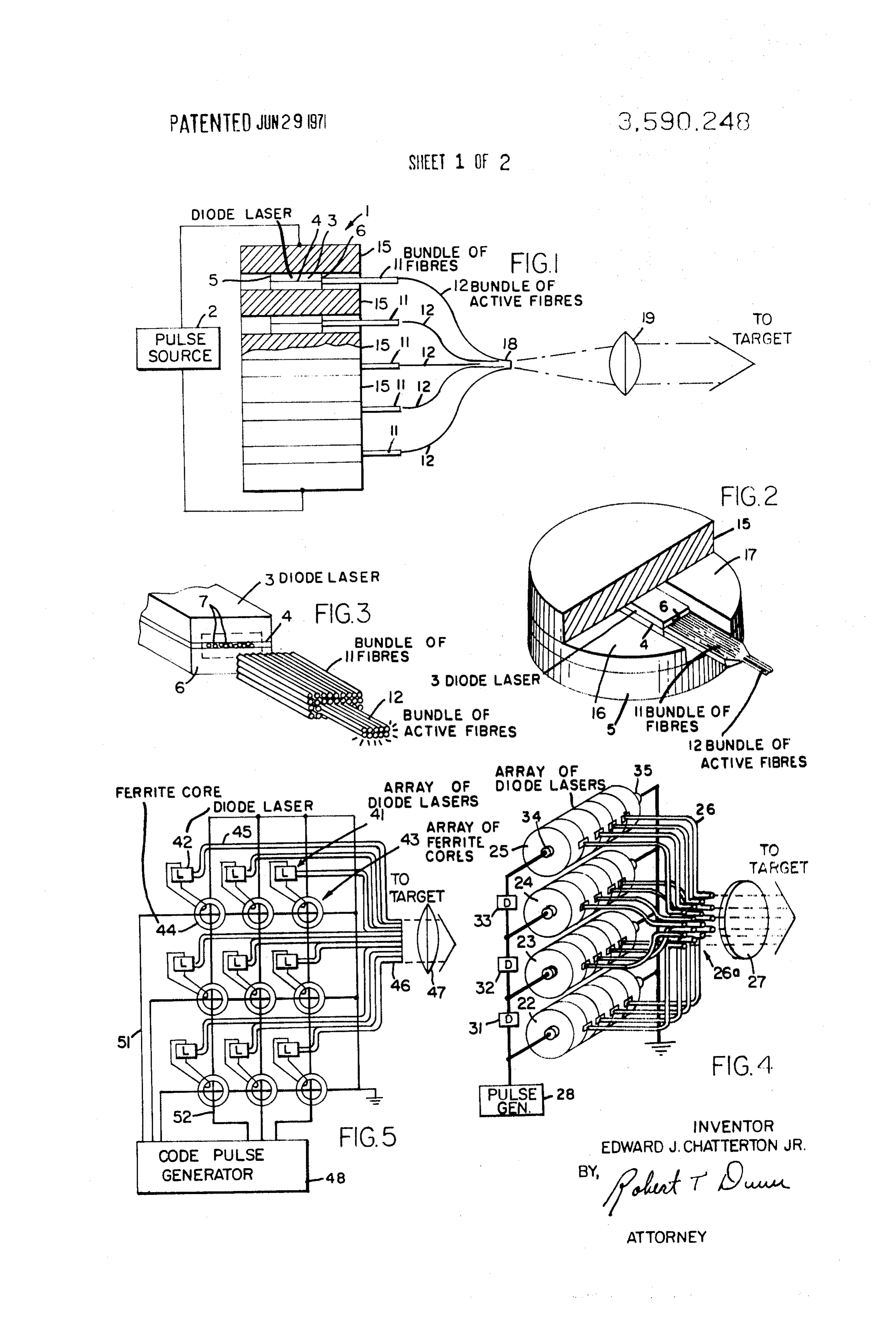
be varied over a relatively broadband of frequencies. Other features and objects of the present invention are ap It is another object of the present invention to provide a parent from the following specific description taken in con wide spectrum source of intense laser radiation. 65 junction with the figures in which; In accordance with a feature of the present invention, a FIG. is a partially sectional view of a stack arrangement or bundle of radiation-conducting tubes or fibers is disposed linear array of diode lasers, each including a bundle of radia abutting one of the optical faces of a semiconductor laser such tion conducting fibers adjacent one optical face thereof, as a GaAs diode laser. During operation, only certain spots in selected active fibers from each of the bundles being com the plane of the diode junction become active and produce the 70 bined to form a single bundle of all active fibers for launching intense laser radiation which emerges from the optical face radiation to a target;
and is conducted by one or more of the fibers in the bundle. FIG. 2 is a detailed sectional view of one of the diode laser Thus, only certain fibers in the bundle are active and conduct elements forming the stack of FIG. 1; the intense laser radiation. These active fibers are selected and FIG. 3 illustrates the relative orientation of a typical one of combined together to form a second substantially smaller bun 75 the diode lasers and fiber bundles;
Page 5
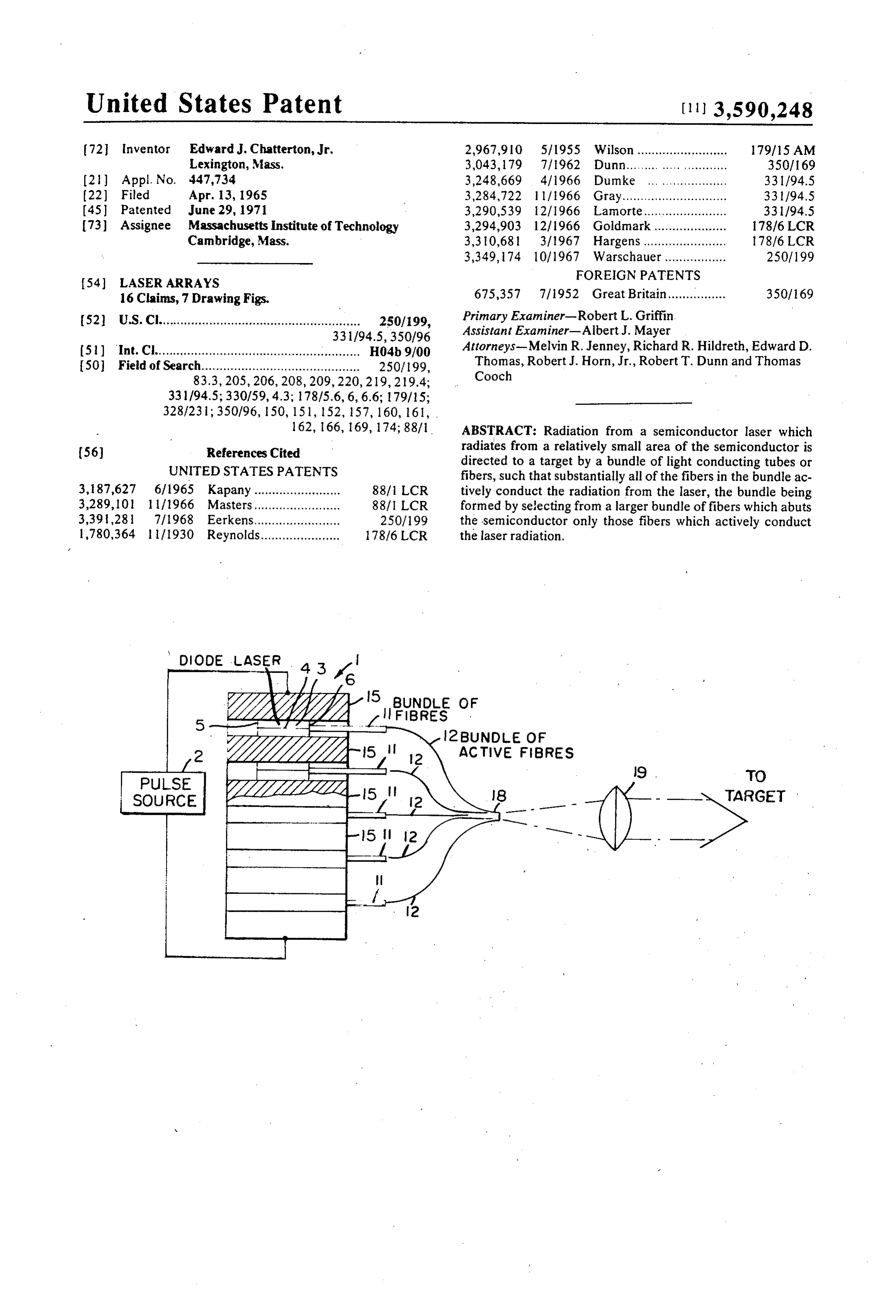
FIG. 3 illustrates an embodiment of the invention employ The embodiment illustrated in FIG. includes a number of ing a plurality of diode lasers with active bundles of fibers issu injection diode lasers stacked together between copper wafers ing from each and arranged in an orderly array so that when 25. Also disposed between the copper wafers on each side of the diodes are energized in sequence, the radiation issuing the diode laser are semicircular wafers of insulating material from the bundles is caused to sweep a target; 5 i6 and 17 which may be fabricated of GaAs. A bundle of F.G. 5 illustrates a laser wavelength-multiplex system in fibers such as bundle ii extends from each of the diodes and cluding a plurality of different types of diode lasers which are from each of these bundles are selected the bundle of active energized in accordance with coded or information signals fibers such as bundle A2, All of the bundles of active fibers are from a number of channels so that the combined bundle of ac combined together to form an output bundle 18 from the tive fibers attached to the diode lasers simultaneously O stack of diodes as shown in FIG. i. The radiation emanating launches radiation to a target of different wavelength each of from the output bundle 8 is directed by a suitable optical which identifies a different channel; system 19 to a target.
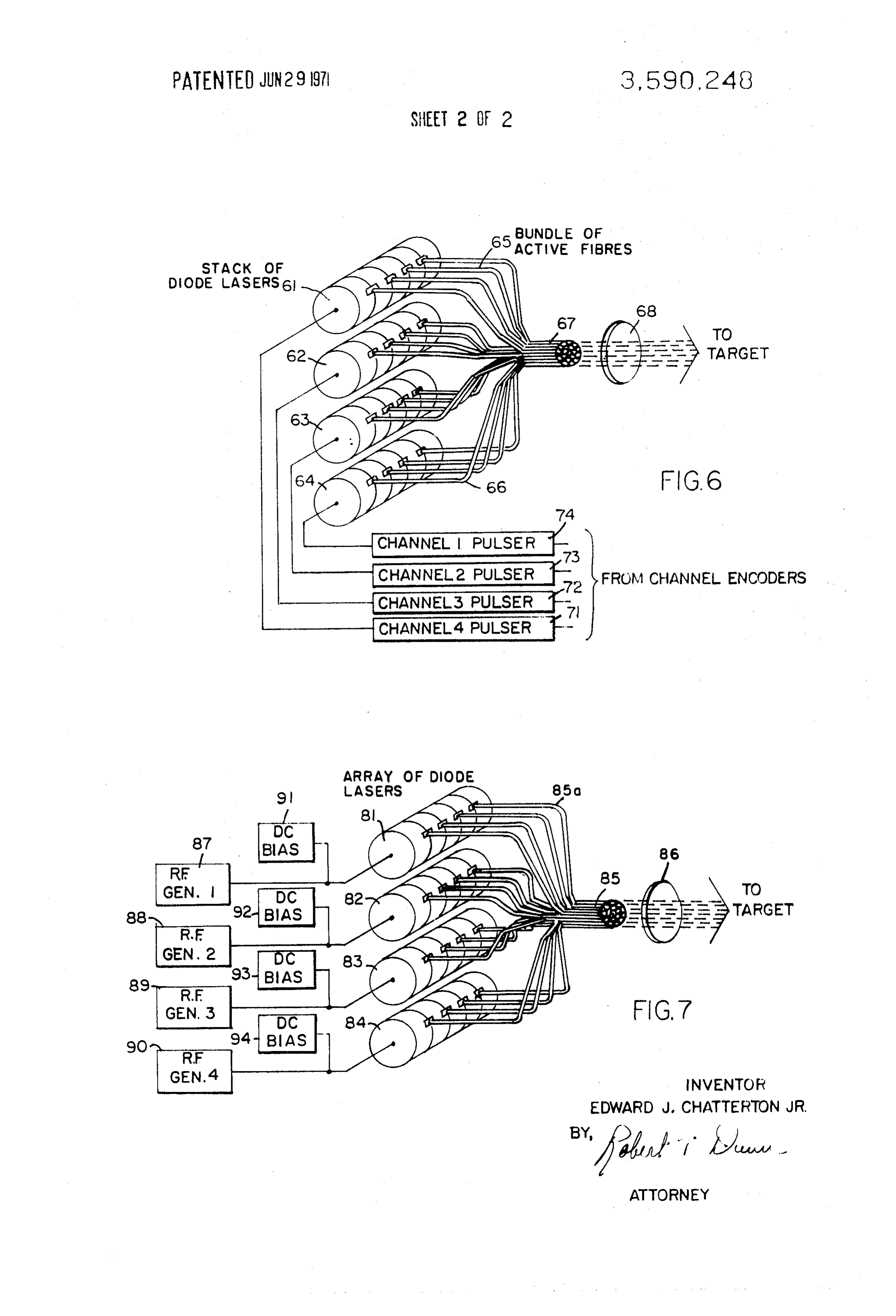
FIG. 6 illustrates a laser time or pulse-multiplex system in A number of compromising considerations are made in a which the different channels are identified at the target by system such as illustrated in FIG. and depend upon the use distinguishing different pulse rates, and 5 that is made of the system. For example, they depend upon the FIG. 7 illustrates a laser frequency-multiplex system in distance to the target and the amount of beam broadening that which the different channels are identified at the target by is permitted in view of the purpose of illuminating the target. distinguishing RF modulation. A practical design of such a system seeks the best compromise Turning first to FIG. , there is shown a linear array of between efficiencies of collection and conduction by the fiber diode injection lasers arranged in a stack and energized by bundles, the required F number of the optical system 19, the current pulses from a source 2. Each of the diodes such as number of fiber bundles that can be accommodated in view of diode 3 consist of a thin chip of semiconductor material such the beamwidth of the system and the equivalent lens diameter as, for example, GaAs in which a diode junction 4 is formed by of the optics. Each use of such a system requires detailed con any of the techniques well known in the art. Optically parallel sideration. Approximately 70 percent of the light incident on faces 5 and 6 are provided on each of the chips to define an 25 optical cavity enclosing the junction plane and substantially the fiber bundles is transmitted by the bundles and approxi mately 10 percent of this is lost in the fibers. Thus, overall transverse thereto. Thus, the axis of the cavity is coincident transmission efficiency to an F/5.6 optic system is better than with the plane of the junction 4 so that coherent radiation 57 percent. In view of this estimated minimum 57 percent from filaments produced at the junction when the diode is transmission efficiency of the fiber optics, radiant power from energized emerges from at least one of the optical faces such various arrays of diode lasers can be computed for several as face 6. Typical filaments of radiation as subtended by the practical telescope sizes and this can be compared with the optical face 6 are shown as spots 7 in FIG. 3. radiant power from a single diode laser. The tabulation below A bundle 1 of 10- to 20-micron diameter glass fibers are shows the relationships between desired beam width, several disposed normal to the optical face 6 of the diode. In some ap practical telescope sizes and the maximum permissible plications, it is desirable to fuse together the fibers in the bun 35 number of diode lasers in the array. die adjacent the face 6 and to cement this end of the bundle directly to the face 6 of the diode. The cross section area of Primary optics Beam the end of the bundle ; ; is substantially greater than the active diameter, f75.6 system
diodes 0.2 mrad mrad
cross section area of the junction and is preferably of the same order of magnitude as the cross section of the diode chip. 40 1. 3 Thus, all laser radiation produced in the junction and concen 50 8. 20 trated in the filaments 7 is gathered by the bundle 1 and is 4, 585 35 183 conducted by active fibers 12 in the bundle. As can be seen, the above table contemplates arrays includ The junction 4 of the GaAs diode is generally about 10 microns thick and the width of this junction is about 0.01 45 ing hundreds and even thousands of diode lasers. Some elec inches. As is well known, during operation, only certain spots trical and thermal problems arise when such large numbers of on the optical face 6 of the junction transmit laser radiation diode lasers are arranged in an array of relatively small physi because the laser radiation is generated in narrow filaments cal size. For example, consider an array of 100 diode lasers. across the junction. These spots corresponding to the fila That is 100 diode lasers stacked one upon another just as illus ments are denoted 7 in FIG. 3. The active spots may extend 50 trated in FIGS. 1 to 3. A structure results which is approxi along as much as two-thirds the total junction width and so the mately 1.5 inches long and 0.2 inches in diameter. The bulk active area of the junction, as subtended by the optical face 6, resistance across the stack into which the pulse source may be about 10 microns by 0.006 inches or a total area of operates is about 10 ohms. Such a structure is amenable to about 1,500 microns square. coaxial feed since the .5-inch length is only one-eighth of a After fabrication of the diode and connection of the diode 55 wavelength of the high frequency component (about 1 K mc. optical face with the bundle of fibers, the active fibers are and so reasonably well-shaped pulses of about 10 nanoseconds selected with the aid of image converters or other suitable de width may be achieved.
tectors and the inactive fibers in the bundle are cut off so that The thermal problems can be resolved as follows. The cylin a smaller bundle of all active fibers such as bundle 12 is drical stack 1.5 inches long and 0.2 inches in diameter can formed. It is preferable that the cross section area of these ac 60 readily dissipate 20 watts into liquid nitrogen in which the tive fibers be somewhat larger than the active area of the junc Stack is immersed during operation producing an internal tem tion, for example about 2,000 microns squared. The radiation perature rise of about 50 K. This estimation of heat dissipa which issues from the active bundle 12 leaves each fiber of tion is very conservative and as a practical matter greater heat that bundle ideally at the angle of incidence of radiation enter can be dissipated with less internal temperature rise by em ing the fiber adjacent the face 6 of the diode. The radiation 65 ploying more sophisticated thermal design such as fins, etc. from a typical GaAs injection diode laser is an irregular beam A multitude of diode laser arrays such as the array illus pattern of approximately 10. The wide angle results from dif trated in FIG. are combined to provide an electrically con fraction from the 10-micron diameter filaments in the active trolled beam scanning laser system such as illustrated in FIG. junction region. If fibers of 10 microns in diameter are em 4. A multitude of the linear arrays or diode stacks 22 to 25 are ployed, further broadening of the beam by diffraction is not 70 arranged as shown to effectively provide a two-dimensional appreciable because the fibers are about the same size as the array of diode lasers. The active fiber bundles 26 from each of thickness of the active region. If smaller fibers are employed, the lasers are arranged to define a two dimensional array of there will result more efficient interception and propagation rows and columns at their ends 26a at the focal point of an op of the radiation, however, it will result in a greater beam tical system 27. In operation, each of these linear arrays 22 to broadening. 75 25 are pulsed in sequence. The pulses are derived from a pulse
Page 6
S 6 generator 28 having its output coupled directly to the linear energize the diode producing a brief burst of radiation which array 22 and coupled through delay circuits 31 to 33 to the ar is conducted from the diode by a bundle of active fibers such rays 23 to 25 as shown in the figure. Each of the delay circuits as bundle 45. The bundles 45 are gathered to form a larger 31 to 33 serve to delay the pulses the same interval. Thus, the bundle 46 which launches radiation through a suitable optics array 23 is pulsed one interval after the array 22, the array 24 5 system 47 toward a target. The active fiber bundle 45 and the is pulsed two intervals after the array 22, and the array 25 is manner of coupling it to the diode laser 42 is preferably of the pulsed three intervals after the array 22. The pulses from the sort already described above with reference to FIG, 3. generator are preferably of very short duration so that as each In operation of the system in FIG. 5, information signals one of the linear arrays is pulsed, the individual diode lasers 1 O such as, for example, binary numbers, are applied to the code which form the array are sequentially energized one after pulse generator 48. This generator produces pulses in ap another along the length of the stack. If, for example, a typical propriate leads which couple to the array of cores 43 so that a one of the linear arrays includes 100 diodes, stacked in a selected one of the cores is energized, the energization being structure a few inches long, the pulse rate is preferably on the of sufficient magnitude to cause the particular laser diode cou order of no more than about 12 Kmc. so that the interval 5 pled thereto to be energized. For example, if the binary value between pulses is at least equal to the pulse propagation time 2 were applied to the generator, electrical leads 51 and 52 through the array. In addition, it is preferred that the pulse would be energized. As a result, there would be a change in length or duration be less than the pulse propagation time the magnetization of all of the cores in one row and one between adjacent diode lasers in the array. This, of course, in column of the array. However, the magnetization of only core sists that the pulses be very short (about 0.1 nanosecond) so 44 would be of sufficient magnitude to produce lasering action that they do not straddle more than a few diode lasers in the in the diode laser coupled thereto so as to energize the laser. linear array at a time. The high frequency components of such Radiation at the characteristic frequency band produced by a short pulse attenuate substantially through the array and the diode laser 42 would then be directed to the target by the thus deteriorate the pulse. To avoid this, impedances such as fiber bundle 46 and, thus, transmit information thereto cor 34 and 35 which are relatively high compared to the im 25 responding to the binary number 2. This illustrates only one pedance across the array are coupled to the circuit at each end technique for energizing the multitude of different types of of an array. laser diodes in controlled fashion so that the wavelength can As an alternative, in order to permit energization with much be controlled and/or switched in accordance with information longer pulses and thereby avoid the problem of high frequency signals. Obviously, more than one of the diode lasers in the component attenuation, each of the arrays 22 to 25 can be array 41 may be energized at the same instant and so more constructive with electrical delays disposed in circuit between than one different wavelength band of laser radiation may be the diode lasers in the array. If, for example, 1 microsecond directed to the target at the same instant and simultaneously delays are used, the energization pulses can be a few detected at the target. The number of different bits of infor microseconds long. These conditions are generally preferred mation that can be transmitted just through different com so that the lineal arrays 22 to 25 are energized in sequence and 35 binations of wavelength bands from the array of lasers is very so that the individual diode lasers in each array are energized large. For example, if an array of 100 lasers were employed, in sequence one or a few at a time. When this is achieved, the the number of such bits is at least 10,000. radiation emanating from the ends of the bundles of active The structure in FIG. 5 can also be employed to generate a fibers 26 arranged in the pattern defined by their ends 26a will 40 laser beam which spatially sweeps a target. For this purpose, it spatially sweep the target in a regular pattern somewhat is, required that the bundles such as 45 be arranged in a pattern similar to the well-known TVraster. such as the pattern defined by the ends 26a of active fiber bun The structure illustrated in FIG. 4 is intended to represent dles 26 in FIG. 4. The pattern is preferably the same as the only one system employing features of the invention for pattern of arrangement of the ferrite cores 43 and diodes 41. producing a laser beam which spatially sweeps a target in an 45 In operation, the spatial sweep may be accomplished by orderly fashion, the nature of the pattern which is swept by the sequentially energizing the cores in a row, one row after beam being determined by the orientation of active fiber bun another. The cores in turn energize the diode lasers 41 in the dles which emanate from a multitude of laser diodes and also same sequence and so the radiation issuing from the pattern of determined by the sequence in which the diodes are ener- . bundles spatially sweeps the target. This technique for produc gized. The structure is useful, for example, to search an area of 50 ing the sweeping laser beam is more versatile than the space for the target so that echoes from the target may be de technique shown in FIG. 4 because the sweep pattern can be tected by detecting equipment and the time coincidence of the varied by merely changing the sequence in which the ferrite echoes compared with the energization intervals of the diode cores are energized. For example, for any fixed two-dimen lasers to determine position coordinates of the target in this sional orientation or pattern of the fiber bundles, it is possible space. This, however, is only one example of a use for the 55 to program the sequence of energization of the cores to device and many others become apparent to those familiar produce just about any laser beam scan pattern desired. The with the art. scan pattern may be cartesian, polar or spiral, and can be For some purposes it is desirable to direct intense laser changed from one to another by merely changing the pro radiation to a target and to switch or change the bands or band gram.
of wavelengths from instant to instant which are directed to 60 The structures described above accomplish beam scanning the target in accordance with information signals thereby by energizing the diodes at successive intervals. This is transmitting the information to the target. Suitable wavelength somewhat the same as time multiplexing. One simple type of band sensitive devices such as phototubes or diode detectors time-multiplexing sets up different channels on the same together with suitable wavelength filters may be employed at transmission path by employing different pulse codes to distin the target to distinguish the different wavelength bands which 65 guish the different channels. For example, the spacing are transmitted and thereby determine the information. FIG. 5 between pulses in pairs of pulses is different from channel to illustrates one such device, including features of the present channel. This technique is sometimes called pulse multiplex invention for transmitting information in this manner. As illus ing and is readily implemented employing features of the in trated in FIG. 5, a plurality 41 of different types of injection vention.
diode lasers such as diode laser 42 are arranged in an array in 70 A pulse multiplexing transmission system is illustrated in correspondence with an array 43 of ferrite cores such as fer FIG. 6. Included are four linear arrays or stacks of diode lasers rite core 44, each of the diodes being energized by electrical 61 to 64. Each array is constructed substantially as described coupling to a different one of the cores. The cores are ar above with reference to FIG. 1. However, the arrays are ranged in regular rows and columns as illustrated and they are 75 pulsed at different rates or by pulse pairs with different time energized in a well-known manner so that when energized, an intervals between pulses. Thus, each array puts forth pulses of electrical pulse is generated in the circuit coupling the core to radiation with a characteristic of distinguishing interval one of the diodes and this pulse is of sufficient magnitude to between pulses. The bundles of active radiation conducting
Page 7
7 ()
fibers such as bundles 65 and 66 are gathered together to form body, said intercepted radiation being conducted by substan a single large bundle 67 of active fibers from which the intense tially less than all of said tubes, and a smaller bundle of said laser radiation is directed by a suitable optical system (68 radiation conducting Subes including substantially only those toward a target. tubes from said first-mentioned buindle which conduct said In operation, four pulsing circuis 71 to 74 which are trig radiation, whereby substantially all of the tubes in said smaller gered by signals from channel encoders, generate pulses at dif bundle conduct radiation.
ferent rates or time separation and of suitable width as 2. A radiation-producing device comprising a body of required for the proper energization of the associated array of semiconductor material, means for defining an optical cavity diode lasers. These pulse width requirements have already been discussed above with reference to FIG. 4. Thus, in opera O enclosing at least a portion of said body of semiconductor material, means for directing energy to said body of semicon tion, all four arrays may be energized at the same time in ductor material whereby an inversion of energy states occurs response to information signals from the encoders in each of in said material accompanied by the production of substan the four channels. As a result, pulses of radiation are launched tially coherent radiation by a process of simulated emission, a from the single bundle 67 along a single path to the target, the 15 bundle of radiation-conducting tubes disposed with their ends pulses being a composite of the four different groups of pulses adjacent said optical cavity so as to intercept substantially all which represent the four channels. At the target, the channels of the portion of said radiation emanating from said optical are distinguished by detecting different pulse rates or spacings cavity, said intercepted radiation being conducted by substan between pulses employing any of the techniques already well tially less than all of said tubes, and a smaller bundle of said known in the art.
20 radiation-conducting tubes including substantially only those
A similar embodiment to that in FG. 6 but which incor tubes from said first-mentioned bundle which conduct radia porates the principle of frequency multiplexing is illustrated in tion from said cavity, whereby substantially all of the tubes in FIG. 7. The linear arrays 81 to 84 in this case may be substan said smaller bundle conduct radiation. tially the same as the arrays 22 to 25 in FIG. 4. However, just 3. A radiation-producing device comprising a body of as in the pulse-multiplexing system of FIG. 6, the bundles of 25 semiconductor material, a PN junction in said body, means for active fibers such as 85a and 85b are all gathered into a single defining an optical cavity enclosing at least a portion of said relatively large bundle 85 from which radiation is launched junction, means for directing energy to said body of semicon toward a target and directed by an optical system 86. The dif ductor material whereby an inversion of energy states occurs ference lies in the method for energizing the arrays. As shown, in said material accompanied by the production of substan each of the linear arrays 82 to 84 is energized by a different 30 tially coherent radiation at said junction by a process of stimu RF generator, the RF signal being imposed on a biasing signal. lated emission, a bundle of radiation conducting tubes For this purpose, RF generators 37 to 90 operating at different frequencies are provided and the output from each generator disposed with their ends adjacent said optical cavity so as to intercept substantially all of the portion of said radiation is DC biased by a separate one of biasing circuits 91 to 94. The emanating from said optical cavity, said intercepted radiation
DC bias in each case energizes all the diodes in the associated being conducted array so that the DC bias combines with the RF signal imposed by substantially less than all of said tubes, thereon to drive the diodes to laser intensity synchronized and a smaller bundle of said radiation-conducting tubes in with the excursions of the RF. The wave propagation time cluding substantially only those tubes from said first-men between adjacent diodes is preferable equivalent to only a tioned bundle which conduct radiation from said cavity, whereby substantially all of the tubes in said smaller bundle fraction of a cycle of the RF and so the diodes in any one of 40 conduct the arrays produce intense laser radiation at substantially the radiation.
same phase interval of the associated RF. 4. A radiation-producing device comprising a multitude of In operation information signals from different channels separate bodies of semiconductor material, means for direct modulate the different RF generators which in turn modulate 45 ing energy to each of said bodies of semiconductor material of the intensity of the total radiation from the linear arrays of sufficient intensity to produce radiation therein, a plurality of diode lasers. Thus, information from several channels is trans bundles of radiation-conducting tubes, each bundle abutting a mitted over the same path between the large bundle 85 of ac different one of said bodies, so as to intercept a substantial tive fibers and the target. The channels are distinguished at the portion of the radiation emanating therefrom, said intercepted target employing suitable band pass filters tuned to the dif 50 radiation being conducted by substantially less than all of said ferent RF. tubes, a second plurality of bundles of radiation-conducting This completes the description of various embodiments of tubes, each including substantially only those tubes from the present invention, all including an array or multitude of among said first plurality of bundles which actively conduct semiconductor laser devices in which lasering action occurs radiation when the associated body of semiconductor material within a volume of the semiconductor material of very small 55 is energized and means for directing radiation emanating from dimensions and including a bundle of a multitude of minute said second plurality of bundles to a target. radiation-conducting fibers disposed at one end of the laser 5. A radiation-producing device comprising a multitude of device so as to intercept and conduct radiation which separate bodies of semiconductor material, means for direct emanates from within the semiconductor material, the ing energy to each of said bodies of semiconductor material number of said fibers being substantially greater than that 60 producing an inversion of energy states therein accompanied required to intercept all of the radiation emanating from the by the emission and amplification of radiation by the process device so that only those fibers which conduct laser radiation of stimulated emission, means associated with each of said can be selected and arranged in a single bundle including all bodies of semiconductor material for defining an optical cavi active fibers for directing the combined radiation from the ty, each of said cavities enclosing at least a portion of one of multitude of lasers to a target. Various embodiments of the in 65 said bodies of said semiconductor material, a plurality of bun vention, all including the above features are described to illus dles of radiation-conducting tubes, each bundle abutting a dif trate some of the uses of the invention. However, these are ferent one of said cavities, so as to intercept a substantial por made only by way of example and do not limit the spirit and tion of the radiation emanating therefrom, said intercepted scope of the invention as set forth in the accompanying claims. radiation being conducted by substantially less than all of said I claim: 70 tubes, a second plurality of bundles of radiation-conducting 1. A radiation-producing device comprising a body of tubes, each including substantially only those tubes from semiconductor material, means for directing energy to said among said first plurality of bundles which actively conduct body of sufficient intensity to produce radiation therein, a radiation when the associated body of semiconductor material bundle of radiation conducting tubes disposed to intercept a is energized and means for directing radiation emanating from substantial portion of said radiation emanating from said 75 said second plurality of bundles to a target.
Page 8
6. A radiation-producing device comprising a multitude of bands in the radiation emanating from said relatively large separate PN junction in semiconductor material, means for bundle of radiation conducting tubes is indicative of said in directing energy to each of said junctions producing an inver formation.
sion of energy states therein accompanied by the emission and 11. A device for producing a wavelength-multiplexed laser amplification of radiation at said junction by the process of 5 beam and directing said beam to a target comprising a plurali stimulated emission, means associated with each of said junc ty of binary energizing devices, separate semiconductor laser tions for defining an optical cavity, each of said cavities en device coupled to each of said binary devices, said laser closing at least a portion of said junction, a plurality of bundles devices being of different kinds producing different of radiation-conducting tubes, each bundle abutting a dif wavelength bands of radiation when energized and a separate ferent one of said cavities, so as to intercept a substantial por 10 bundle of radiation-conducting tubes, optically coupled to tion of the radiation emanating therefrom, said intercepted each of said semiconductor laser devices, one end of said bun radiation being conducted by substantially less than all of said dles of radiation-conducting tubes being arranged to form a tubes, a second plurality of bundles of light-conducting tubes, relatively large single bundle, means for controlling said bi each including substantially only those tubes from among said 5 nary devices in response to information signals so that said dif first plurality of bundles which actively conduct radiation ferent semiconductor laser devices are energized producing when the associated body of semiconductor material is ener combinations of said wavelength bands in the radiation gized and means for directing radiation emanating from said emanating from said relatively large bundle of radiation con second plurality of bundles to a target. ducting tubes which is indicative of said information. 7. A device for producing a spatially scanning beam or 12. A device producing a wavelength-multiplexed laser radiation comprising a plurality of semiconductor laser beam and directing said beam to a target, comprising an or devices, a plurality of separate bundles of radiation-conduct derly array of ferrite cores, a separate semiconductor laser ing tubes each associated with a different one of said semicon device coupled to each of said cores, said laser devices being ductor laser devices and arranged in an orderly relationship, of different kinds producing different frequency bands of means for energizing said plurality of devices in a predeter 25 radiation when energized and a separate bundle of radiation mined sequence and an optical system for intercepting and conducting tubes optically coupled to each of said semicon directing radiation emanating from the ends of said bundles of ductor laser devices, one end of said bundles of radiation-con light-conducting tubes, the order of energization of said radia ducting tubes being arranged to form a relatively large bundle, tion-producing devices, the arrangement of said ends of said means for energizing said ferrite cores in response to informa bundles of tubes and the positions of the ends of said bundles 30 tion signals so that the wavelength bands of radiation emanat in said optical system being such that a beam of radiation is ing from said relatively large bundle of radiation conducting directed from said optical system to sweep an area of space in tubes are indicative of said information. a predetermined manner. 13. A device for producing a multiplexed laser beam com 8. A device for producing a spatially scanning laser beam prising a plurality of semiconductor laser devices, a plurality comprising a plurality of semiconductor laser devices, a plu 35 of bundles rality of separate bundles of radiation-conducting tubes each pled at one ofendradiation-conducting with a different one tubes each optically cou of said laser devices, the associated with a different one of said semiconductor laser devices and each formed from a larger such bundle by selec other ends of said bundles being formed into a single bundle of radiation-conducting tubes, a plurality of different communi tion of active tubes therein, said plurality of separate bundles 40 cation being arranged in an orderly relationship, means for energiz channels, each coupled to a different group of said laser ing said plurality of semiconductor laser devices in a predeter channelsfor devices for energizing said devices, means in each of said generating information signals, means in each of mined sequence and an optical system for intercepting and directing radiation emanating from the ends of said bundles of said channels for energizing the associated group of laser radiation-conducting tubes, the order of energization of said devices in a manner characteristic of said channel, signals semiconductor laser devices, the arrangement of said ends of 45 from different channels, a means for detecting radiation which issues from said single bundle and means associated with said said bundles of tubes and the positions of the ends of said bun detecting means for distinguishing said characteristic manners dles in said optical system being such that a beam of laser of energization, thereby distinguishing said different informa radiation is directed from said optical system to sweep an area tion channels.
of space in a predetermined manner.
9. A device for producing a spatially scanning laser beam 50 14. A device for producing a pulse-multiplexed laser beam comprising a plurality of semiconductor laser devices, a plu comprising a plurality of semiconductor laser devices, a plu rality of separate bundles of radiation-conducting tubes each rality of bundles of radiation-conducting tubes each optically associated with a different one of said semiconductor laser coupled at one end with a different one of said laser devices, devices and each formed from a larger such bundle by selec 55 the other ends of said bundles being formed into a single bun tion of active tubes therein, said plurality of separate bundles dle of radiation conducting tubes, means for energizing dif being arranged in an orderly series of rows and columns, ferent groups of said laser devices by different pulse trains in means for energizing said plurality of semiconductor laser response to information signals from different channels, devices in a predetermined sequence row after row down a means for detecting radiation which issues from said single column and an optical system for intercepting and directing 60 bundle and means associated with said detecting means for radiation emanating from the ends of said bundles of radiation distinguishing said different pulse trains thereby distinguishing conducting tubes to a target, whereby a beam of laser radia said different information channels.
tion is directed from said optical system to sweep said target in 15. A device for producing a frequency-multiplexed laser a regular manner. beam comprising a plurality of semiconductor laser devices, a 10. A device for producing a wavelength-multiplexed laser 65 plurality of bundles of radiation-conducting tubes each opti beam and directing said beam to a target comprising a plurali cally coupled at one end with a different one of said laser ty of semiconductor laser device, means for energizing each of devices, the other ends of said bundles being formed into a sin said laser devices, said laser devices being of different kinds gle bundle of radiation conducting tubes, means for energizing producing different wavelength bands of radiation when ener said laser devices, means for modulating the energization of gized, a separate bundle of radiation conducting tubes opti 70 different groups of said laser devices at different frequencies cally coupled to each of said semiconductor laser devices, one in response to information signals from different channels, end of said bundles of light-conducting tubes being arranged means for detecting radiation which issues from said single in a relatively larger bundle, means for controlling the bundle and means associated with said detecting means for sequence of energization of said laser devices in response to distinguishing said different frequencies thereby distinguishing information signals so that combinations of said wavelength 75 said different information channels.
Page 9
16. A device for producing a spatially scanning laser beam ferent one of said semiconductor laser devices for energizing comprising a plurality of semiconductor laser devices, a plu said laser devices and means for energizing said ferrite cores, rality of separate bundles of radiation-conducting tubes each whereby laser radiation from said laser devices is conducted bundle having one end optically coupied with a different one by said bundles of radiation conducting tubes and launched of said semiconductor laser devices, the other ends of said from said other ends into space spatially scanning an area bundles being arranged in an orderly array, a plurality offer thereof.
rite cores, means coupling each of said ferrite cores to a dif
Provenance
- Collection
- Cited prior art
- Original PDF
- patentimages.storage.googleapis.com →
- Filed
- 1965-04-13
- Pages
- 9
- Method
- pdftotext (the PDF's own text layer) + pdftoppm 300dpi page scans
- Source
- Google Patents bibliographic record
- Granted
- 1971-06-29
- Inventors
- Edward J Chatterton Jr; Massachusetts Institute of Technology
- Transcribed from
- patentimages.storage.googleapis.com →