patent · US5393351
Multilayer film multijunction thermal converters
28 February 1995
Page 1 — bibliographic record
United States Patent (19) 11. Patent Number: 5,393,351 Kinard et al. 45 Date of Patent: Feb. 28, 1995 54 MULTILAYER FILM MULTIJUNCTION Over the Frequency Range DC to 100 kHz', IEEE, THERMAL CONVERTERS vol. IM-21 (1972), F. J. Wilkins, pp. 130-136. (75) Inventors: Joseph R. Kinard, Darnestown; "A Proposal for a Multijunction Thermal Converter', Dexiang Huang, Gaithersburg; G. Yonezaki et al., IEEE Transactions on Instrumenta Donald B. Novotny, Bethesda, all of tions and Measurement, vol. 18, No. 2 (1989), pp. Md. 338-341.
"Accurate Radio-Frequency Microvoltages' Selby;
73) Assignee: The United States of America as (1953), pp. 158-164.
represented by the Secretary of "Accurate Thin Film Multijunction Thermal Converter Commerce, Washington, D.C. on a Silicon Chip', M. Klonz et al., IEEE, Transactions 21 Appl. No.: 3,905 on Instrumentation and Measurement, vol. 38, No. 2
22 Filed: Jan. 13, 1993 "Monolithic Thermal Converter', P. O'Neill, p. 12. 5ll Int. Cl............................................. HOL 35/04 Primary Examiner-Donald P. Walsh 52 U.S. C. .................................... 136/225; 136/200; Assistant Examiner-Chrisman D. Carroll 136/203; 136/204; 136/205; 136/211; 136/212; Attorney, Agent, or Firm-Lowe, Price, LeBlanc &
58 Field of Search ............... 136/200, 203, 204, 205, 57 ABSTRACT
216 Multijunction thermal converters are formed in an inte gral multifilm membrane form over a through opening 56) References Cited in a nonmagnetic, dielectric substrate. Through the use
niques, very compact, rugged and precise integrated 839,985 l/1907 Briston ................................ 136/227 structures are formed to include either single linear 1,390,743 9/1921 Alicutt 136/227 2,937,218 5/1960 Sampietro ... 136/4 elongate heater elements, bifilar or trifilar heater ele 3,607,445 9/1971 Hines ................................... 136/225 ments, and multijunction thermopiles at reasonable cost. 3,715,288. 2/1973 Riggin ............................. 204/38 A Disposition of the heater element and hot junctions of the thermopiles over a through opening in the substrate,
(List continued on next page.) with the coldjunctions of the thermopiles disposed over the substrate thickness, enables the heating element to
FOREIGN PATENT DOCUMENTS provide a substantially isothermal uniform heating of
the thermocouple hot junctions to obtain high thermal.
58-171873 10/1983 Japan ....... . . 136/225 efficiency and reduce Thompson and Peltier heating 61-53530 3/1986 Japan ................................... 136/213 effects. Forming the essential elements into an inte 64-29721 1/1989 Japan ................................... 136/200 grated multifilm membrane also makes possible minimi 64-64268 3/1989 Japan ................................... 136/200 zation of interconnections between the elements, and 1-199481 8/1989 Japan ................................... 136/200 this results in minimized reactance. The resulting ther
OTHER PUBLICATIONS
mal converters are relatively inexpensive and rugged, have high sensitivity, superior ac-dc and RF-dc perfor “Thermal Conductivity and Diffusivity of a Thin Film mance characteristics, and provide broader bandwidth SiO2-Si3N4 Sandwich System”, F. Volklein, Electron performance than is possible with conventional devices. ics and Optics, Thin Solid Films 188 (1990), pp. 27-33.
“Theoretical Analysis of the AC/DC Transfer Differ ence of the NPL Multijunction Thermal Convertor 24 Claims, 9 Drawing Sheets
fash'? mill situasis.
2) TERHOLE EAL
EAER
A contact PA
Sis
Page 2
- - - -- 4,665,276 5/1987 Elbel et al........ ... 136/215 3,767,470 10/1973 Hines ................................... 1.36/225 4,677,416 6/1987 Nishimoto et al. ................... 338/35 3,979,226 9/1976 Renner et al. ... 136/208 4,850,713 7/1989 Thery et al. ...... ... 374/30 4,111,717 9/1978 Baxter ........... ... 136/225 4,953,387 9/1990 Johnson et al. ... ... 73/25.03 4,211,888 7/1980 Stein et al. ... 136/225 4963,195 10/1990 Kadato et al. .... ... 136/225 4,257,822 3/1981 Gomez ...... ... 136/206 4,969,956 11/1990 Kreider et al. ... 136/201 4,276,441 6/1981 Wilson ... ... 136/206 4,971,632 11/1990 Rowe. ... 136/212 4,363,927 12/1982 Wilson .......... ... 136/206 4,983,225 1/1991 Rowe ................ ... 136/201 4,456,919 6/1984 Tomita et al. . 357/28 A 5,056,929 10/1991 Watababe et al. ... 374/181 4,465,895 8/1984 Verner et al. . ... 136/225 5,059,543 10/1991 Wise et al. .............................. 437/3 4,558,342 12/1985 Sclar......................--------...-- 357/30 5,100,479 3/1992 Wise et al. .......................... 136/225

Page 3
Drawing sheet — no readable text.
Page 4
Drawing sheet — no readable text.
Page 5
Drawing sheet — no readable text.
Page 6
Drawing sheet — no readable text.
Page 7
Drawing sheet — no readable text.
Page 8
Drawing sheet — no readable text.
Page 9
Drawing sheet — no readable text.
Page 10
Drawing sheet — no readable text.
Page 11
Drawing sheet — no readable text.
Page 12
difference to exist between the junctions. This voltage
MULTILAYER FILM MULTIJUNCTION difference, which the typical thermocouple is con THERMAL CONVERTERS structed to use, is temperature-dependent and is known in the art as the "Seebeck effect’. If the materials used
FIELD OF THE INVENTION 5 are conductors or semiconductors, a current will flow This invention relates to multilayer, thin-film, multi through the thermocouple and may be extracted by junction thermal converters (MLF-MJTC) suitable for connection to elements of an external circuit, typically use as primary and secondary calibration standards and through contact pads. When a number of thermocou for the measurement of ac and RF voltage and current O ples are connected in series, to enhance the rather small over a broad frequency range. More particularly, this voltage differences generated in the individual thermo invention relates to MLF-MJTC's which offer perfor couples under certain circumstances, the plurality of mance over very broad ranges of frequency, current thermocouples is referred to as a “thermopile'. Ther range and output emf, with low ac-dc and RF-dc differ mopiles may be used for a variety of purposes, e.g., to ences, in a form suitable for low cost mass production 5 determine a voltage or current, to generate electricity for inclusion in a variety of instruments. from sources of heat such as sunlight received by a solar BACKGROUND OF THE PRIOR ART collector system, or to actuate protective or sensing devices.
Thermal converters are the most accurate instru In light of the variety of uses to which a thermo ments known for the measurement of ac voltage and couple or a thermopile may be employed in a device to current at frequencies ranging from low audio fre-20 quency on up to 1 GHz. Multijunction thermal con convert energy of one form into another, e.g., heat or incident electromagnetic radiation into a current, it is verter structures are most conducive to a wide range of important to clarify the use of the term “converter' as uses. These are frequently used in very high accuracy used in the present application. In the following de ac-dc difference metrology, because they exhibit very scription small ac-dc differences, provide a good square law re- 25 is used toofrefer the present invention, the term "converter' to conversion of each of an ac and then sponse, and high output emfs. In one form or another, a dc signal to heat, such multijunction thermal converters are employed to heat correspondingand in each case to generate from the output electrical signals which are generate primary standards for the National Institute of monitored. In essence, the devices and the methods Standards and Technology (NIST) for ac-dc difference, ac voltage and current, and ac power and energy cali 30 described more fully hereinbelow relate to generating electric energy from a very precisely controlled source bration services.
The basic MLF-MJTC structure includes a heater of heat energy, this being accomplished by the provi element, a plurality of cooperating thermocouples con sion of a very precisely formed and operated electrical nected in series, i.e., one or more thermopiles, and elec ly-powered heater element and selectively disposed sets trical wiring connecting the MLF-MJTC to an external 35 of thermocouples with their hot junctions heated by the circuit or known types of voltage, current and power heater.
measurement devices. In addition to the basic MLF Very precise standards for determining a voltage or MJTC structure, one or more resistors connected to current over a wide range of frequencies for ac-dc and heater element to receive input voltage and/or current. RF-dc applications are necessary for an MLF-MJTC. Preferably, the thermopiles are electrically insulated To meet this need, an MLF-MJTC requires physical from the heater element to ensure high response accu ruggedness, ability to withstand stresses associated with racy, i.e., so that an unknown signal will not flow into thermal cycling and in-use exposure to a wide range of the circuit which is used to monitor the thermopiles (or temperatures locally, and an error-free structure, e.g., even into the thermopiles themselves) as this would minimization of capacitances or inductances developed produce an error. 45 between the heater and thermopiles. In the past, thermal converter structures have typi Such devices may be used to measure the power or cally included fine wires of different conductive materi calibrate the energy of radiated signals from optical als to form sets of thermocouples carefully located with sources, e.g., infrared sources or lasers. This operation respect to each other and the heater element. There are relies on the physical principle that when radiation is significant problems in physically handling the very fine 50 incident on the invention a certain percentage of it is wires that are combined to make such thermocouples absorbed and the heater region of the invention is and in soldering or otherwise affixing them to each heated, thus producing a change in its emf output that is other and to the rest of the structure. An example of proportional to the incident energy. The measurement such an early structure is disclosed in U.S. Pat. No. of this output can be used to determine the power or 839,985 to Bristol, titled “THERMOELECTRIC 55 energy of the incident radiation.
GENERATOR’. Also, the measurement of vacuum, pressure or air More recently, a variety of thermocouples and ther flow can be accomplished with the present invention. mal converter structures have been designed for spe This operation is permitted by the physical principle cific applications through the use of thin film and thick that the amount of heat lost by convection when oper film technologies. ated at a constant power is proportional to the pressure Regardless of which physical form is selected, i.e., and gas flow. The number of molecules striking the whether wires or thin films deposited by any known heated surface and leaving it per second is proportional technique are employed, the principal physical phenom to either the pressure or the flow of the gas over the enon being exploited depends on the fact that when surface. By measuring the temperature, which is in different thermal electric materials are joined at their 65 versely proportional to the thermal loss, which in turn is spaced-apart ends, with the junctions located in regions inversely proportional to either the pressure or gas at different temperatures, the difference in the internal flow, the pressure or gas flow can be measured. It is electron structures of the two materials causes a voltage noted that these two properties are not measured at the
Page 13
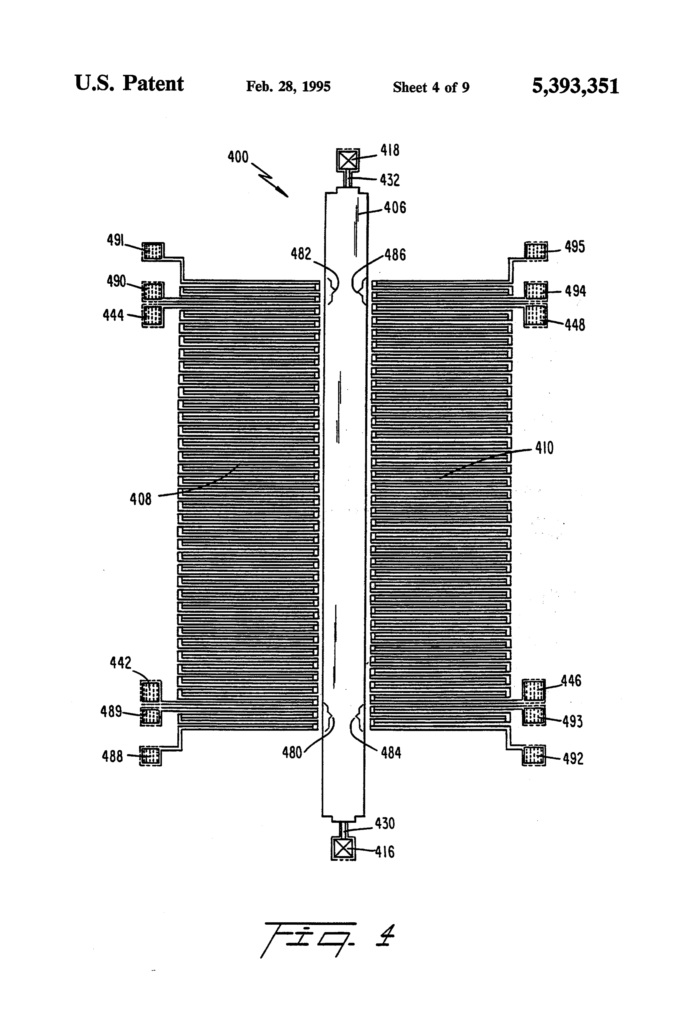
same time. Consequently, pressure is measured when metrically disposed thermopiles with contact pads pro there is no significant gas flow and vice versa. vided for electrical connections thereto. In order to maximize the accuracy of MLF-MJTC, it FIG. 3 is a transverse cross-sectional view, at Section is necessary that the Thompson coefficient of the heater III-III in the embodiment of the MJTC per FIG. 2. material be small, and the thermocouples be disposed 5 FIG. 4 is a plan view of a second coaxial embodiment uniformly and symmetrically on opposite sides of the which includes more numerous thermocouples disposed elongated heater element. Low Peltier effect is also coaxially, i.e., symmetrically on opposite sides of the necessary for enhanced operation as exemplified by the single elongate heater element with their respective hot present invention. To achieve this result the contact junctions relatively close to the heater element, with area between the heater and the contact pads should be 10 guard thermocouples provided at both ends of the sets on a good heat sink such as a silicon frame. of thermocouples, with the guard thermocouples being These and other related objects of this invention are provided with their own contact pads for selective described more fully hereinbelow, as are structural electrical engagement therewith.
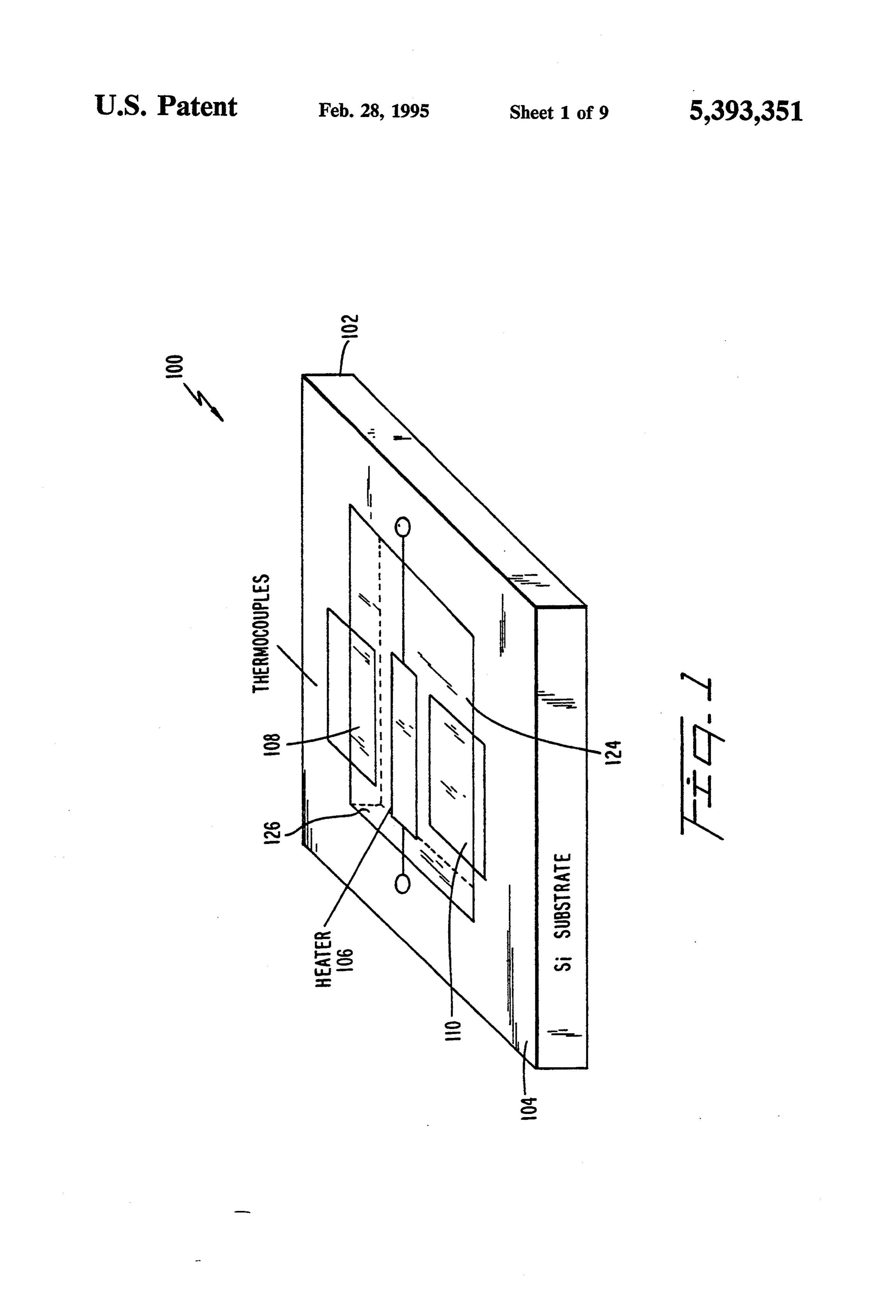
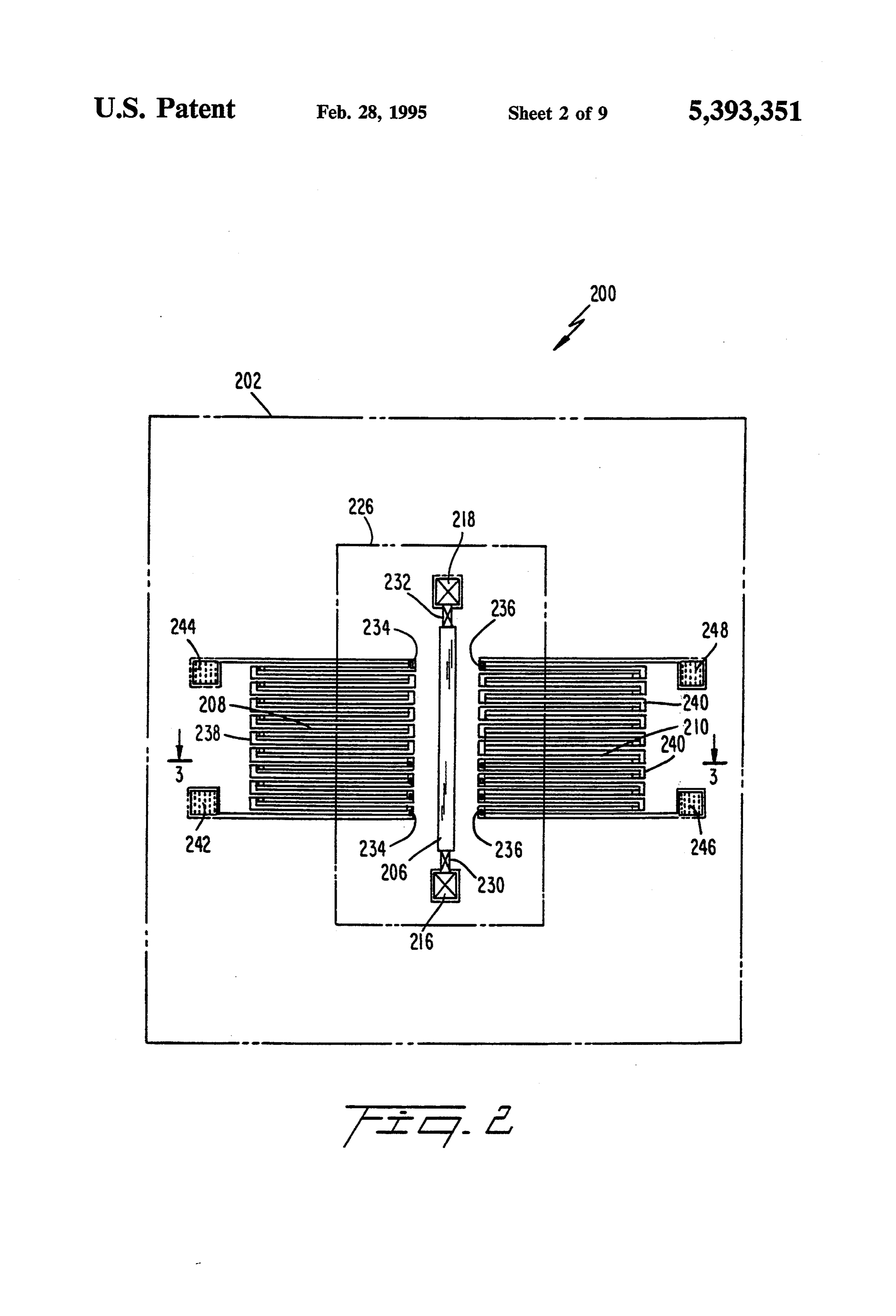
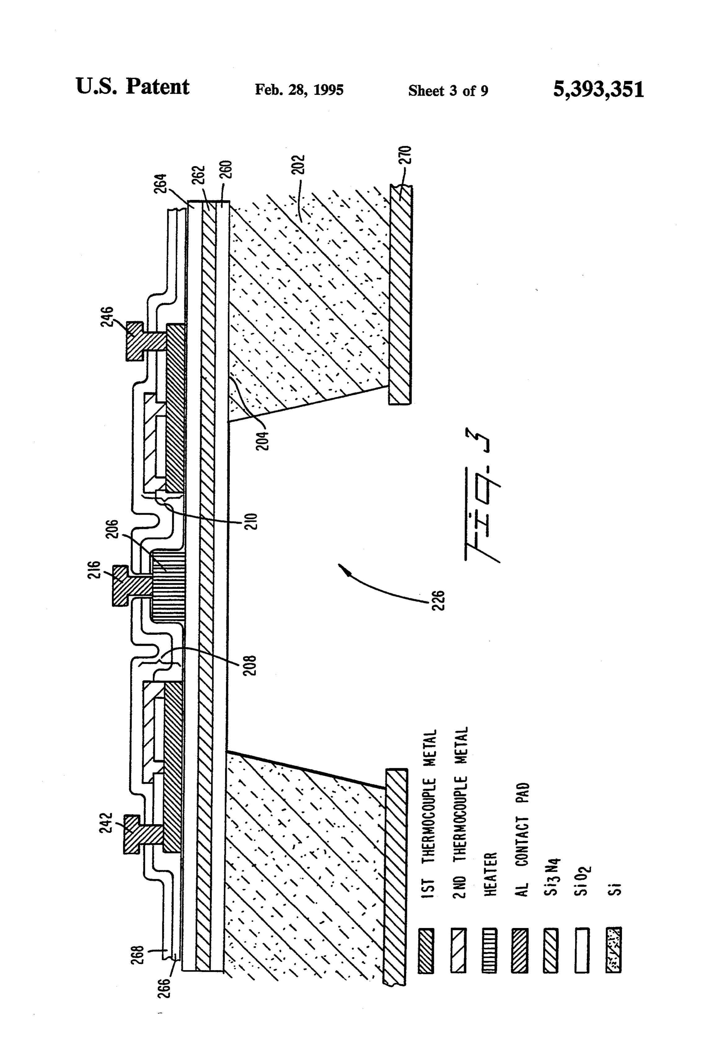
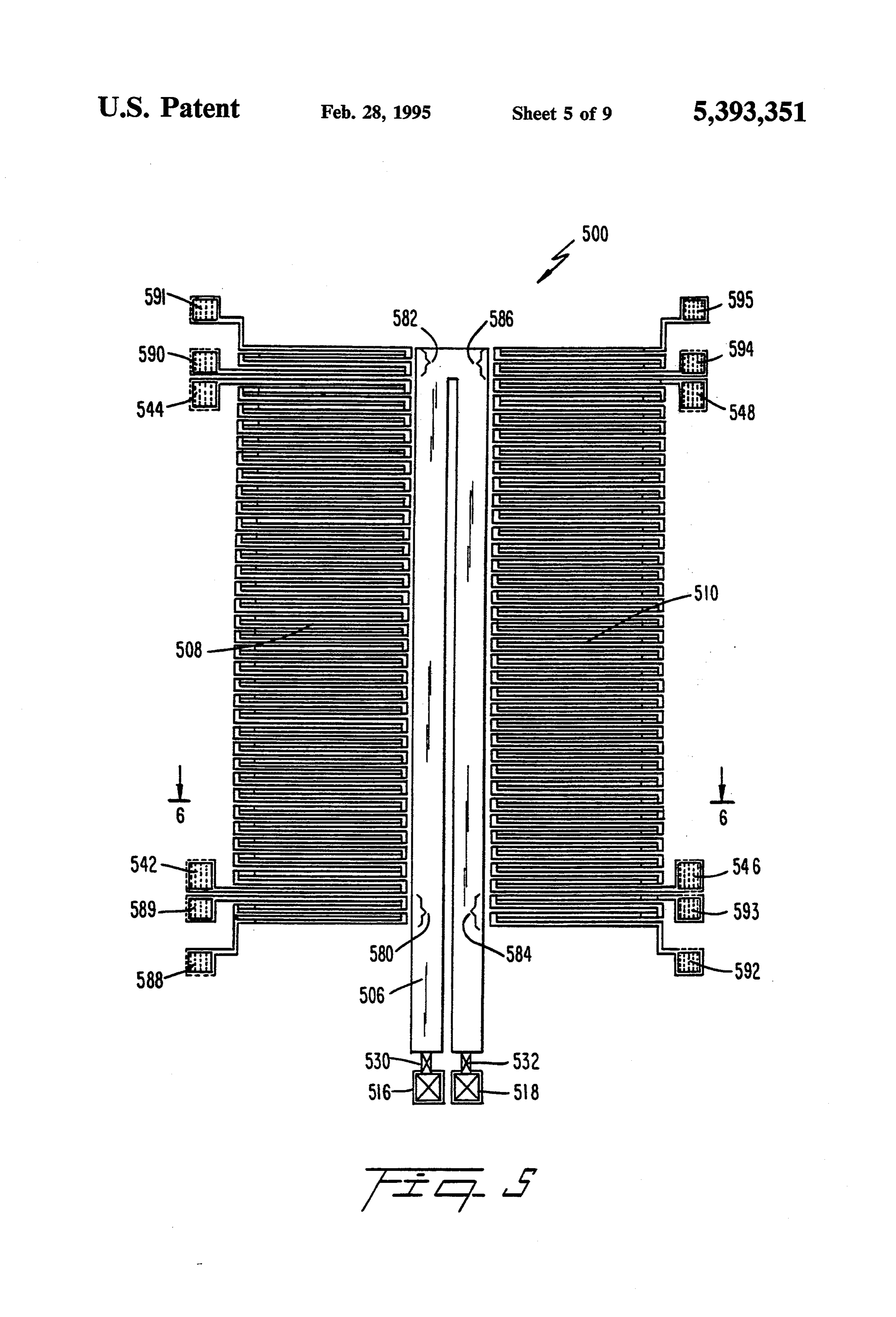
details of the preferred embodiments of this invention FIG. 5 is a plan view of an MLF-MJTC having a and methods of forming the same. Persons of ordinary 15 structure skill in the art, upon understanding the following disclo per FIG. 4generally except similar to that of the MLF-MJTC for a bifilar heater element axially of sure and the accompanying drawing figures may con two sets of symmetrically disposed thermocouples and sider implementing obvious modifications and varia guard couples.
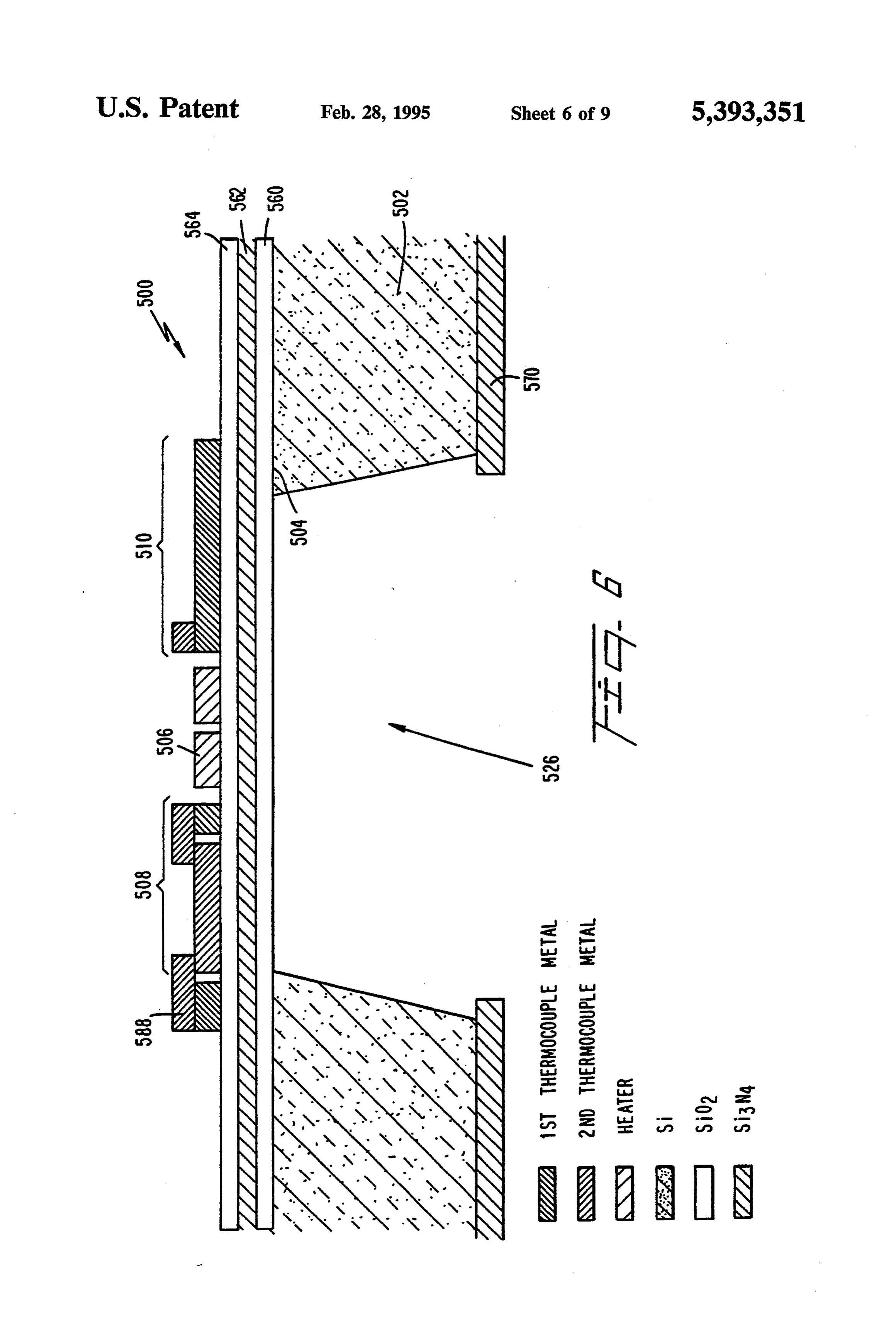
tions of this invention, and the claims appended hereto FIG. 6. is a transverse cross-sectional view at Section are intended to comprehend such variations of the ex 20 VI-VI in the embodiment of the MLF-MJTC per plicitly disclosed embodiments. FIG. 5.
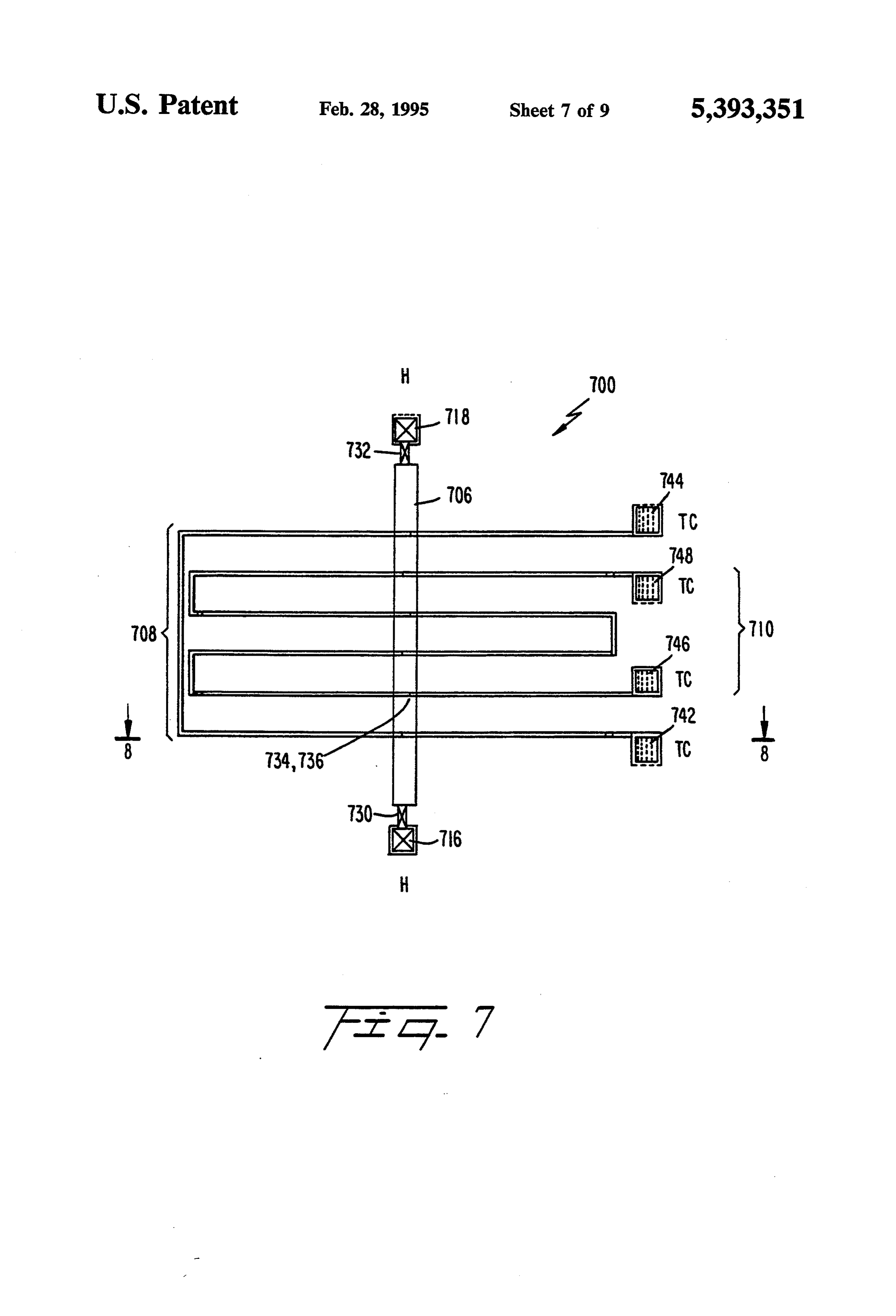
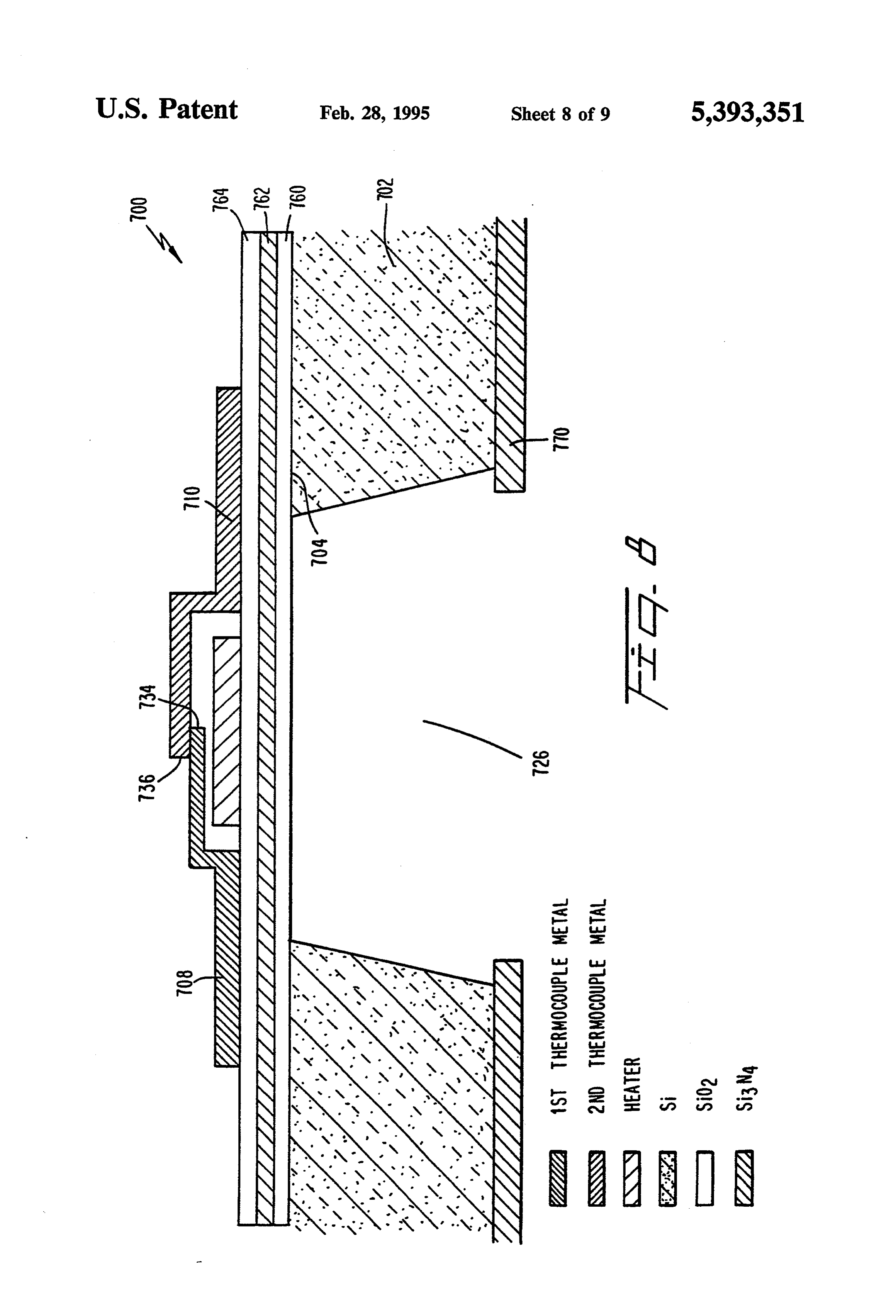
SUMMARY OF THE INVENTION FIG. 7 is yet another embodiment according to this A principal object of the present invention is to pro invention, wherein only a small number of thermocou vide highly compact, inexpensive, easy to manufacture, 25 ples are incorporated within an MLF-MJTC which comprises a single elongate heater element in which the rugged, durable, multilayer thin-film multijunction hot junctions of individual thermocouples are disposed thermal converters MLF-MJTCs to measure alternat ing current, and voltages, at frequencies ranging from immediately above the single heater element. low audio frequencies to 1 GHz. FIG. 8 is a transverse cross-sectional view at Section Another object of the present invention is to provide 30 VIII-VIII in the embodiment of the MLF-MJTC per MLF-MJTCs for high accuracy ac and dc difference FIG. 7.
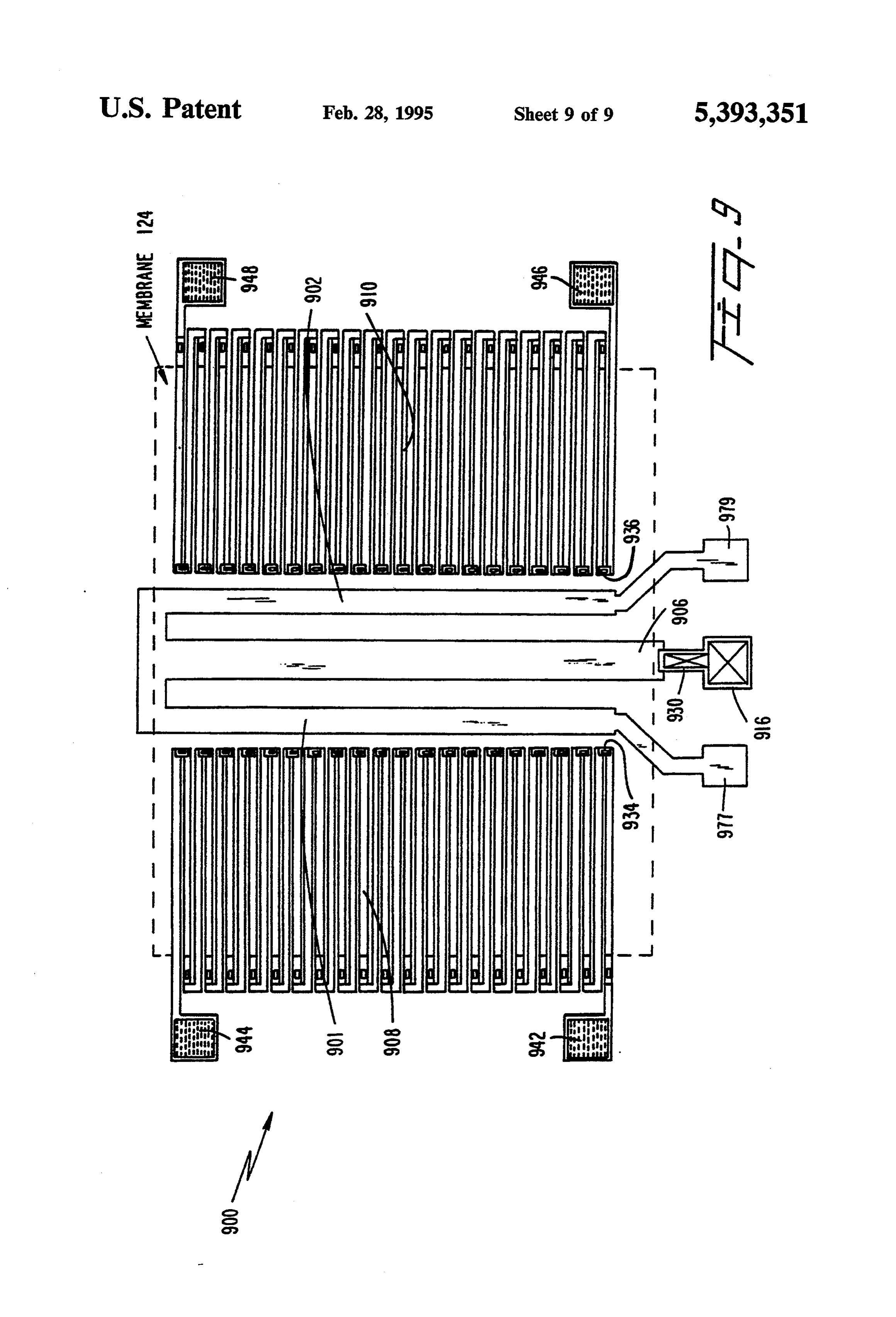
measurements with very low ac-dc differences and FIG. 9 is a plan view showing a trifilar heater ar good square law responses with high output emfs, with rangement.
additional thermocouples optionally provided for test DETAILED DESCRIPTION OF THE ing and guard functions. 35 PREFERRED EMBODIMENTS Yet another object of this invention is to provide low-cost, highly reliable, mechanically stable, low and An essential requirement of a high performance high current MLF-MJTCs, including either a single or MJTC is that it should have a heater element with a a bifilar heater element on a composite, stress-balanced, small heater resistance. The heater should therefore be thin-film membrane. 40 thin and small, and should also have a very low distrib A related further object of this invention is to provide uted inductance and capacitance to ensure that the a method for forming the above-described type MLF ac-dc difference at high frequencies is small. The ther MJTC structures to provide the desired precise mea mocouples in such an MLF-MJTC also must be formed surement capabilities. of thin layers and must be geometrically precisely made These and other objects of this invention are realized 45 and disposed with respect to the heater element to en by providing an MLF-MJTC having a substrate with a sure that there is a uniform temperature distribution membrane on it. The membrane consists of a first layer within the heater to ensure a small ac-dc difference. of SiO2, second layer of Si3N4 and a second SiO2 layer Ideally, the heater structure should be one in which the all formed over an aperture or a through hole in the temperature of the entire heater element is uniform. substrate. A layer of electrically resistive material is 50 Such a heater would have very low errors due to provided on a mounting surface formed of the three Thompson effect.
membrane layers. A first set of serially-connected thin Experience in the manufacturing of semiconductor film thermocouples is formed to have their cold junc devices has led to the development of photolitho tions over the substrate which serves as a heat sink and graphic techniques which enable the formation of ex their hot junctions arrayed side by side overlying the 55 tremely precise and regular geometries of thin-film aperture on one side of the heating element. A second elements such as the heater elements, thermocouples, plurality of serially-connected thin-film couples is resistor elements and contact pads. Such techniques, formed on the opposite side of the heating element with spanning both thin-film and thick-film technologies, cold junctions over the substrate and hot junctions over together with a planar structure for the devices, are the aperture. 60 found to satisfy the above-stated objects of this inven tion.
BRIEF DESCRIPTION OF THE DRAWINGS A preferred composition of the alloy used to form the FIG. 1 is a perspective view of the multilayer film heater element, available commercially as "Evanohn', multijunction thermal converter (MLF-MJTC) of the is as follows:
present invention. 65 nickel 75%
FIG. 2 is a plan view of an MLF-MJTC according to chromium 20% a preferred coaxial embodiment of this invention, which aluminum 2.5% includes a single elongate heater element and two syn copper 2.5%
Page 14
Suitable materials for forming thermocouples are: ferred combination of steps to form the desired struc “Constantan” (40% Cu and 60% Ni) and “Chromel” tural layers will now be described. Details of the vari (10% Cr and 90% Ni ), and many others. ous elements which cooperate to form various embodi The contact pads are preferably made of a highly ments of the MLF-MJTCs follow.
conductive metal, e.g., aluminum, copper, or even gold As generally indicated in FIG. 1, the heater element if cost and other considerations are not limiting. 106 is thermally isolated by its location on a thin dielec The materials employed to form the thermocouples, tric membrane 124 which stretches across and over an pads, etc., are preferably applied by sputtering. Other opening 126 formed in silicon substrate 102. The hot alternatives include evaporation of the selected materi junctions of each thermopile 108,110 are disposed sym als or printing with ink containing the same. Any af 10 metrically in close thermal proximity to heater element fordable and reliable known apparatus or technique for 106. The cold junctions of each of the thermocouples forming uniform thin films may be utilized. The pre comprised within thermopiles 108,110 are, correspond ferred structure eventually includes an integrated plu ingly, symmetrically disposed to be on a portion of the rality of films, including dielectric layers formed of thin dielectric film which is an extension of the thin materials such as SiO2 and Si3N4, preferably applied by 15 dielectric membrane 124 and which stretches over the a known technique such as chemical vapor deposition, silicon substrate 102 to provide good thermal contact organic reduction, evaporation, plasma enhanced depo therewith. Dielectric membrane 124 is actually a multi sition, or sputtering. film composite formed in successive steps over an ini One of the keys to forming the high-efficiency MLF tially continuous silicon substrate 102, i.e., the dielectric MJTCs according to the present invention is to produce 20 membrane. 124 is formed or partially formed before low-stress, multilayer films. One of the other keys is the opening 126 is created.
formation of thin-film thermocouples. To do this, ini First, a silicon substrate 102 of suitable size and thick tially, a heat sink (not shown) is attached to the back of ness is anisotropically etched from the lower or rear a silicon wafer 102 to keep it at close to room tempera surface by any conventional technique so that its thick ture. Selected materials for the heater element 106, the 25 ness is reduced in the region in which opening 126 is to thermocouples 108,110, assorted insulation layers and be formed, the etching leaving a thickness of silicon in the small contact pads (not shown) with low capaci the range 10 to 100 um. This reduced thickness portion tance are then applied and patterned with the use of is to provide initial support for the dielectric membrane masks and photolithographic techniques. 124 which is to be formed thereover in the course of In order to reduce the capacitance current, flowing in 30 fabricating the thermal converter structure. Then, after parallel with the heater current from the contact pads, the thermal converter structure is completely fabri and thereby improve the performance for accurate ac cated, the remaining thickness of the silicon substrate in current and multirange ac voltage measurements, small the region of opening 126 is entirely etched away, leav pad areas (50x50 m2 to 400X400 um2) are used. This ing the thermal converter as an integral part of the is necessary for bifilar heater arrangements, coaxial 35 dielectric membrane and supported by it. This requires heater arrangements and high frequency MLF-MJTC precise alignment of any masks used in the etching of devices. However, pad size is not critical for high cur silicon substrate 102 and/or any masks used in defining rent type heaters have lengths from 20 um to 8000 um, and forming the heater element, thermocouples, junc widths of 10 pum to 6000 um and length to width ratios tions, contact pads and the like. To facilitate proper of 0.1 to 10. (It is noted that non-high current MLF alignment, the fabrication employs a two-sided, front MJTC devices normally have lengths of 20 pum to 8000 to-back alignment process, wherein suitably sized win um, widths of 1 pm to 1200 pm and length to width dows are patterned onto the Si3N4 film on the back side ratios of 4 to 800). of a relatively large silicon wafer in alignment with If sputtering is used, the sputtering rate is kept low alignment marks provided on the front side of the wa and is adjusted as needed to ensure that the resulting 45 fer.
structure will have low residual stresses. Other adjust For present purposes, the basic silicon wafer may be able parameters in the process of applying the selected of approximately 100-600 um nominal thickness, pol layers is the distance between the target, i.e., source of ished on both sides. A silicon dioxide film is then grown the material to be deposited, the substrate surface on on both sides thereof to a thickness in the range 100 to which the material is to be deposited and the pressure of 50 700 nm nominal thickness. The term “grown' is used the ambient argon used for sputtering in this case is 1-2 herein to describe a process of oxidizing the silicon mTorr. The through opening 126 is initially formed by wafer surface to produce a strongly adherent silicon etching the silicon substrate 102 in the area formed by dioxide film thereon. As the oxidation process contin this patterned Si3N4 film at the backside from its rear ues, the thickness of the oxide film thus increases or surface part way through the thickness thereof, with the 55 "grows'. Both sides of the silicon wafer are then coated residual thickness of silicon removed by etching only with photoresist and photolithographically patterned so after the key elements, i.e., the heater element 106, the that the patterns on the two sides are aligned with re thermocouples 108,110, etc., are formed. This leaves a spect to each other. The mask to be applied to the front relatively stress-free, stable, strong multi-film structure side of the wafer provides alignment marks and the stretched over the through opening. mask for the back side of the wafer provides definition To minimize problems that would otherwise be gen for etching the openings 126 for a plurality of devices to erated during use of the finished device at the interface be formed from-a single silicon wafer. The alignment of between the heated material of the heater element and the two masks is done in a conventional fixture which the silicon surface contacted thereby and regions imme brings the imaged sides of both the masks together, i.e., diately surrounding the heater, the present invention 65 permits visual observation of both simultaneously, and thus employs a low-stress, multifilm, composite mem also permits controlled lateral movement of the masks brane which has both a high thermal efficiency, low relative to one another until the images are observed to dielectric loss and high mechanical stability. The pre be in desired alignment. The masks are then held in this
Page 15
chosen alignment while separated apart from each A nominal 30 to 500 nm thick CVD LTO film is other, and a wafer provided with photo-resist coatings deposited on the front side of the silicon wafer. On this on both sides is inserted therebetween. The masks are silicon oxide LTO layer, a 30 to 400 nm thick Evanohm then brought together and each side of the photoresist film of low stress is sputter deposited. This Evanohm coated silicon wafer is exposed, thereby transferring film is coated with a photoresistand the heater structure each masked image onto the wafer surface. Other meth is patterned in alignment with the thermocouple hot ods for alignment of both sides can also be used. The junctions formed earlier. The Evanohm is then etched images thus formed are then etched into the silicon in perchloric acid based etchant. The photo-resist is dioxide surface, preferably with buffered hydrofluoric then stripped, the wafer is plasma ashed for several acid. The photoresist is then stripped in conventional 10 minutes in oxygen, and another layer of 20 to 300 nm. manner and a nominal 100 nm to 400 nm thick silicon thick CVD LTO film is then deposited thereover. nitride film is deposited onto the silicon dioxide surface, The surface of the LTO film is then coated with preferably by a known chemical vapor deposition photoresist and windows corresponding to electrical (CVD) process. contact pads are patterned thereon and etched through The nitride film used in the invention is a low stress 15 the LTO layer to enable electrical contacts to be made type, chemically deposited by using a ratio of di to the thermocouples and heater elements. The photore chlorosilane-to-ammonia different from that which is sist is then stripped, the wafer is plasma ashed in oxy normally used for film formation. An excess of about 4:1 gen, and a nominally 100 to 1000 nm thicklayer of pure of DCS:NH3 and at a temperature of 700-900 C. is 20 aluminum is sputter deposited thereon. The aluminum layer is then coated with another layer of photoresist, used.
Both sides of the wafer are coated again with another and an contact pads are patterned thereon and etched with aluminum etchant. This completes the formation of layer of a photoresist, and the original back side mask is aligned to its original image which is now formed in the the low stress, multifilm structure of the typical MJTC. Actually, depending on the selected patterns, a multi silicon dioxide film on the back side of the coated wafer, 25 tude and the photoresist with the mask in place is again ex large of the devices are thus formed on the relatively silicon wafer.
posed. The pattern thus formed on the back side of the Kerfs are cut approximately half way through the silicon wafer is plasma etched through the silicon ni wafer thickness in the streets between individually pat tride coating, preferably with "Freon 114’ gas to form terned devices which are to be diced from the silicon openings (i.e., windows) penetrating through both the 30 wafer. The silicon wafer surface is then protected with silicon nitride and silicon oxide layers down to bare hard black wax, and the remaining 10 to 100 um thick silicon. Note that the front side of the wafer is not thus etched because it is protected by the hitherto unpat ness of the silicon substrate corresponding to the terned photoresist layer. The patterned silicon nitride through openings in each of the devices is etched away film at the rear surface of the wafer now serves as an 35 in hot KOH. The black wax is then removed with xy etching mask to form the openings 126, which are otherand lene the individual devices are separated from each by breaking the relatively larger silicon wafer at etched through the thickness of the silicon wafer to the various kerfs.
within 10 to 100 um of the front surface of the wafer, The above-described process of making MJTCs ac preferably with a 10 to 70% weight aqueous solution of cording to this invention provides devices that have potassium hydroxide held in a temperature range of 40 40 certain very valuable attributes. Thus, for example, to 120 C. with the generally available, high-precision masking A low temperature silicon dioxide (LTO), in a thick and etching equipment now commercially available, the ness of 10 to 400 nm, is then chemically vapor deposited entire planar structure of the device can be formed with on the front surface of the silicon wafer. The Si extremely regular geometry. This is important for the O2-Si3N4-SiO2 sequence provides lower dielectric 45 manufacture of primary standards, which is a principal loss than Si3N4-SiO2-Si3N4, and therefore better objective of this invention. It is also very important that electrical performance of the heater, and reduces the the temperature gradient along the heater element be risk of surface cracks due to defects. very small, i.e., one would ideally like to have a heater On the LTO thin film, a thin film in the range of 30 to structure with an entirely uniform temperature to re 400 nm thickness of low stress “Chromel' is then sput 50 duce errors that may otherwise arise from thermoelec ter-deposited. The surface of the thin “Chromel” film is tric effects like Thompson heating, and the like. Fur coated with photoresist and the first legs of the thermo thermore, the thermopiles formed in precise relation couples which are to provide the thermopiles are ship to the heater element all present essentially a uni aligned to the alignment marks patterned onto the front form thickness of the chosen metals to the elongate surface of the silicon wafer and are patterned into the 55 edges of the heater, so that there is a very uniform resist. The-photo-resist is then cured and the “Chro thermal conduction path along the entire length of the mel' layer is etched in a perchloric acid based etchant. heater and between the heater and the thermopiles sym The photoresist is thus stripped and the surface cleaned metrically disposed in correspondence therewith. This by plasma ashing in oxygen for several minutes. The ensures a very uniform temperature distribution along wafer is then dipped for a few seconds in diluted per 60 the heater length and is important for forming precise chloric acid based etchant to remove any oxide film on standards.
the "Chromel” formed during the oxygen plasma clean The time constant for the typical MLF-MJTC ac ing, washed in deionized water, and dried. A low stress, cording to this invention is in the range 5 to 300 msecs. nominally 30 to 400 nm thick constantan film is sputter This is quite fast compared to what is available in the deposited on the front surface over the patterned 65 known art. A very rapid time constant may not be desir "Chromel'. The "Constantan' is then etched in an able because, if one reduces the frequency of the ac aluminum etchant, the photoresist stripped and the received by the heater element, the heater temperature wafer then plasma ashed for several minutes in oxygen. begins to track the variations of the ac waveform and
Page 16
then one no longer has an acto dc thermal converter. It When used with instrumentation, thermal converters should be remembered that the heat output of a heater may be used to receive an input signal, e.g., an ac input, receiving ac has a thermal output with twice the fre for comparison thereof with some internal reference quency of the input ac because the polarity of the cur such as a known dc reference voltage. The structures rent is irrelevant in generating thermal energy. It should formed according to this invention enable such compar also be remembered that the electrical output of the isons, with very small errors across a much broader thermopiles is proportional to the thermal power gener band width than existing primary standards. Because of ated by the heater element. A thin layer of glass may be the thin-film structures and precise definition of the added to increase the time constant of the device to various elements in the thin films, the thermal convert avoid tracking of the heater power peak frequency by 10 ers according to this invention should provide very the thermopile output, especially at low ac frequencies. high thermal efficiency and, consequently, the need for It is believed that if a high quality dielectric, e.g., very low power inputs. Furthermore, with a large num glass, is used instead of silicon to provide additional ber of thermocouples provided in each of the thermo thermal mass for the MLF-MJTC structures, it should piles, even with very low inputs it should be possible to be possible to increase the thermal time constant even 15 generate signals of the order of 100 mV and, if the de for use of thermal converters down to low audio fre vices are mounted in a vacuum, the sensitivity and then quency or even a little below. If the thermal time con output EMF will be two to ten times higher. stant can be kept short enough, e.g., in the order of 100 The mechanical strength and stability of the MLF to 200 msec it should be possible to have high speed 20 MJTCs is thus ensured by forming them integrated with measurements from a device which works at low audio a membrane which is a composite of silicon oxide la frequencies. No known device exists for such measure mella (in compressive stress), a silicon nitride lamella (in ments. tensile stress), and another silicon oxide lamella (in com Another aspect of the present invention that is partic pressive stress), on which the heater and thermocouple ularly helpful for precise operation is the provision of 25 structures are fabricated. The different stresses of these guard couples at the ends of the heater element, lamellas are "balanced' such that the composite mem whether the heater elements are coaxial or bifilar. Such brane is in a net low stress (i.e., near zero net stress) guard couples are merely thermocouples provided at during use. The compressive stress produced by the silicon oxide lamellas on each side of the nitrate lamella the very ends of the thermopiles to permit a user to are approximately equal and produce very little or no • monitor nonuniformities associated with the end por 30 tendency tions of the heater element structures. These guard is broken to curl the membrane. Thus, if the membrane somehow, it has only a slight curl-up or curl thermocouples are provided with their own contact pads to enable selective use or disuse as desired. In other down tendency at most.
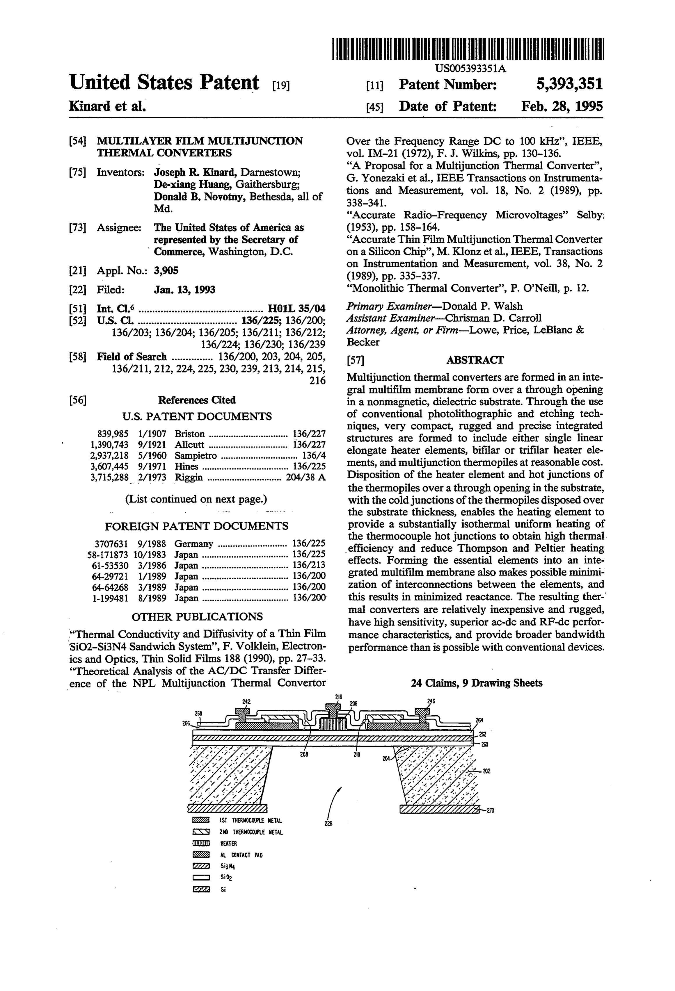
FIGS. 2 and 3 respectively show plan and cross-sec words, the emf corresponding to each guard couple can be monitored separately and may selectively be added 35 tionalMJTC views of a first preferred embodiment of an according to this invention. In the illustrated to the emf of the thermopiles. Although guard thermo MJTC 200, formed on an upper surface 204 of a silicon couples are known in other contexts, it is believed that substrate 202, there is a through opening 226 over they have never previously been included in thin-film which is disposed devices. Their optional inclusion into the MLF-MJTCs 206 connected at itsanends elongate linear flat heater element to contact pads 216 and 218 by according to this invention facilitates more precise com very short, flat, highly conductive pensations to be applied to the thernopile outputs in respectively. Symmetrically disposedlayers on
opposite sides regions where there may be relatively large thermal of heater element 206 are hot junctions 234 and 236 of gradients, i.e., effects associated with the ends of the thermopiles 208 and 210, respectively. Note that hot heater elements. In this manner, selective manipulation of the output from the thermopiles can be used to com 45 junctions 234,236 are close to but physically separate and electrically insulated from heater element 206, and pensate for or make corrections for what are essentially are located above through opening 226. Cold junctions structural limitations. When one is considering the pro 238 and 240, of thermopiles 208 and 210 respectively, vision of primary standards, i.e., when high accuracy is are located over the silicon substrate 202 to be in good the goal, this provides a relatively secure and reliable thermally conductive relationship therewith. Contact solution to providing high quality corrections to the 50 pads 242,244 are provided at the very ends of thermo device output. One can either arrange for an outside pile 208, and contact pads 246,248 are similarly pro circuit to utilize the outputs from the guard thermocou vided for electrical communication with the ends of ples or, in the alternative, one may digitize the respec thermopile 210.
tive data from the guard thermocouples and the princi The heater element is connected in a coaxial arrange pal thermopiles and then apply the necessary correction 55 ment including a connection to a signal source and a to the latter. return path to that source (not shown). The return path Basically, one uses thermal converters by applying an can be located in any number of locations both on and unknown ac and observing the output emf in the ther off the semiconductor substrate. For example, a metallic mopiles, and then applying a known dc and bringing the casing enclosing the MLF-MJTC can be used as a re output to the same level. If the ac/dc difference of the turn path. Return paths can also be located on other thermal converter is zero, so that its performance with mounting structures holding the substrate, as well as on ac is the same as its performance with dc, then one has the substrate.
succeeded in comparing the rms value of the ac to the In FIG. 3 there is a silicon oxide layer 260 applied to corresponding known and precisely measured value of the upper surface 204 of dielectric substrate 202. Sub the dc. In other words, the thermal converter is used to 65 strate 202 is preferably formed of silicon but for some precisely monitor any difference between ac and dc in applications glass may be more suitable. On the silicon the primary standard environment or in the primary oxide layer 260 there is provided a silicon nitride layer calibration laboratory environment. 262 over which is provided a second silicon oxide layer
Page 17
264. As previously noted, heater element 206 is prefera same manner as FIGS. 2 and 3 in accordance with the bly formed of a selected electrical resistance material corresponding description provided above. such as "Evanohm'. Each of the thermopiles 208 and FIGS. 7 and 8 respectively show plan and cross-sec 210 comprise a plurality of serially-connected and geo tional views of a third embodiment of an MLF-MJTC metrically similar thermocouples formed as described 700 according to this invention. In this embodiment, as earlier. The contact pads such as 216, 218 and 242-248 in the previously described embodiments, the linear are all preferably formed of a highly conductive metal, elongate heater element 706 and the hot junctions of the e.g., aluminum or gold. Each of the thermocouples in thermocouples are all located over a through opening thermopiles 208 and 210, as described earlier, comprises 726 in a dielectric substrate 702. However, MLF-MJTC two dissimilar metals joined at a hot junction to be O 700 differs from the previously described embodiments heated by heat generated in the adjacently disposed in that there are fewer thermocouples in the thermopiles heater element 206. Adjacent thermocouples are seri 708 and 710, and the contact pads 742,744, 746 and 748 ally connected at cold junctions 238 and 240 which are therefor are all disposed on the same side of heater in good thermal contact through layers 260-264 with 15 element 706. Furthermore, the hot junctions of the dielectric substrate 202. Additional protective silicon thermocouples are in an overlying relationship over dioxide layers 266 and 268 may be provided (as best heater element 706, as best seen in FIG. 8. The hot seen in FIG. 3). thermocouples can also be arranged under heater ele The immediately preceding paragraphs describe an ment 706. As also seen in FIG. 8, a silicon nitride layer exemplary MLF-MJTC structure suitable for broad 20 770 may be provided on the back surface of dielectric band, high-frequency, primary standards service. This Substrate 702.
It is necessary to have a completely nonmagnetic device has a relatively basic and simple structure. mounting
Other, more sophisticated and somewhat more elabo materials, structure because, in the presence of magnetic the skin effect errors can become noticeable rate MLF-MJTCs are also encompassed by the present in an ac frequency range from a little above 100 kHz up invention. 25 to 10 MHz. With respect to thermal considerations, it FIG. 4 is a plan view of an MLF-MJTC with a linear should be noted that the thermal efficiency of the type elongate flat heater element, two symmetrically dis of multijunctions illustrated in the various figures de posed thermopiles 408 and 410, heater contact pads 416 scribed herein is very high, so that one can operate the and 418 respectively connected to heater element 406 MLF-MJTCs at quite low currents and low voltages by short flat conductors 430 and 432, and thermopile 30 compared to those possible with known types of de contact pads 442-448. In addition, and in a manner vices. Known thermal distinctive over the structure of the previously de very successfully below converters about 1.0 cannot be operated mA. If lower currents scribed embodiment per FIGS. 2 and 3, the MLF are used, one obtains a very low output emf. By con MJTC per FIG. 4 is provided with guard thermocou trast, with the type of multijunctions possible according ples 480 and 482 for thermopile 408 as well as guard 35 to the present invention, the operation can be success thermocouples 484 and 486 for thermopile 410. These fully carried out at currents much lower, and with out guard thermocouples each have respective contact pads put emfs much larger, particularly if the device is vac 488-495, as illustrated in FIG. 4. For simplicity, other uun mounted. It is believed that high accuracy mea details generally similar to those of the previously de surements can thus be made down to the tens of mV scribed embodiment are not illustrated. The manner in level because the thermal efficiency is high. which the guard thermocouples may be utilized to en FIG. 9 illustrates a "trifilar' heater arrangement. This hance the precision and utility of the MLF-MJTC per is a structure in which an ac or dc flow through a cen FIG. 4 was described earlier. tral heater and back to the source is carried out through Consideration must be given to the so-called "skin to on either side of the heater symmetry disposed return effect” which occurs when high-frequency ac flows 45 paths 901 and 902. The return paths can be entirely through a conductor. It is well known that alternating contained within the periphery of the through aperture, current tends to flow along the outer surfaces of the entirely outside the periphery or some combination of conductor instead of the inner bulk thereof. This skin both.
effect is frequency dependent, so that the effective elec With the thin-film multijunctions of the present in trical resistance is different with ac than it is with dc. 50 vention one can choose heater current ratings and Therefore, if one employs thicker heater element resis heater voltage ratings which are tailored to various tances on the MLF-MJTCs, the skin effect becomes applications more readily than is possible with the con significant. The thin-film heater structures described ventional devices. With conventional devices of this herein are designed to have small errors due to skin type, one method employed to obtain an improved effect. This is particularly true in the low voltage 55 isothermal region is to surround the device with a rela - ranges. tively large block of a highly thermally conductive FIGS. 5 and 6 illustrate, in plan and cross-sectional material such as copper. By contrast, with the use of a views respectively, a modified MLF-MJTC 500 which nonmagnetic, thermally conductive ceramic mounting has a bifilar, flat, elongate heater element 506. Note that substrate to hold the MLF-MJTC substrate, the device by this form a much longer electrical resistance element according to the present invention is less bulky, as well is provided between heater contact pads 516 and 518 to as more efficient and rugged. Further improvement in heat the hot junctions of thermopiles 508 and 510. In thermal characteristics is provided by the use of a ce other respects, the structure of MLF-MJTC 500 is gen ramic lid fitted to the mounting substrate enclosing the erally similar to that of MLF-MJTC 400 illustrated in entire MLF-MJTC.
FIG. 4. In FIG. 6, the various layers and elements are 65 In this disclosure, there are shown and described only numbered in a scheme generally comparable to that the preferred embodiments of the invention, but, as employed in FIG. 3. Persons of ordinary skill in the art aforementioned, it is to be understood that the invention should be able to interpretFIGS. 5 and 6 together in the is capable of use in various other combinations and
Page 18
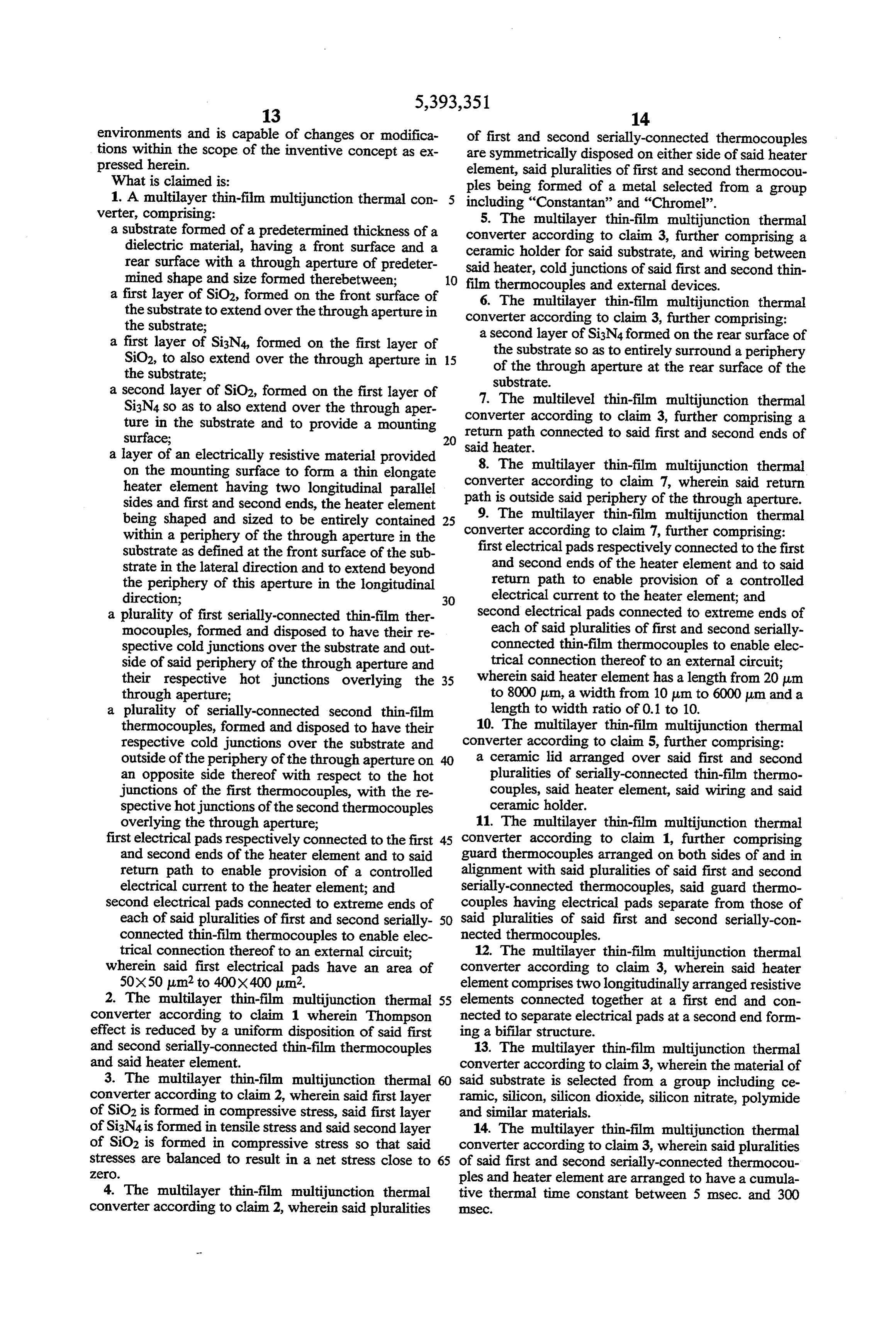
environments and is capable of changes or modifica of first and second serially-connected thermocouples tions within the scope of the inventive concept as ex are symmetrically disposed on either side of said heater pressed herein. element, said pluralities of first and second thermocou What is claimed is:
1. A multilayer thin-film multijunction thermal con 5 ples being formed of a metal selected from a group including “Constantan” and "Chromel”.
verter, comprising: 5. The multilayer thin-film multijunction thermal a substrate formed of a predetermined thickness of a converter according to claim 3, further comprising a dielectric material, having a front surface and a ceramic holder for said substrate, and wiring between rear surface with a through aperture of predeter said heater, cold junctions of said first and second thin mined shape and size formed therebetween; 10 film thermocouples and external devices. a first layer of SiO2, formed on the front surface of 6. The multilayer thin-film multijunction thermal the substrate to extend over the through aperture in converter according to claim 3, further comprising: the substrate; a second layer of Si3N4 formed on the rear surface of a first layer of Si3N4, formed on the first layer of the substrate so as to entirely surround a periphery SiO2, to also extend over the through aperture in 15 of the through aperture at the rear surface of the the substrate; substrate.
a second layer of SiO2, formed on the first layer of 7. The multilevel thin-film multijunction thermal Si3N4 so as to also extend over the through aper ture in the substrate and to provide a mounting converter return path according to claim 3, further comprising a connected to said first and second ends of
a layer of an electrically resistive material provided said8. heater.
The multilayer thin-film multijunction thermal on the mounting surface to form a thin elongate converter according to claim 7, wherein said return heater element having two longitudinal parallel path is outside said periphery of the through aperture. sides and first and second ends, the heater element being shaped and sized to be entirely contained 25 9. The multilayer thin-film multijunction thermal within a periphery of the through aperture in the converter according to claim 7, further comprising: substrate as defined at the front surface of the sub first electrical pads respectively connected to the first strate in the lateral direction and to extend beyond and second ends of the heater element and to said the periphery of this aperture in the longitudinal return path to enable provision of a controlled direction; 30 electrical current to the heater element; and a plurality of first serially-connected thin-film ther second electrical pads connected to extreme ends of mocouples, formed and disposed to have their re each of said pluralities of first and second serially spective cold junctions over the substrate and out connected thin-film thermocouples to enable elec side of said periphery of the through aperture and trical connection thereof to an external circuit; their respective hot junctions overlying the 35 wherein said heater element has a length from 20 um through aperture; to 8000 pum, a width from 10 um to 6000 pm and a a plurality of serially-connected second thin-film length to width ratio of 0.1 to 10. thermocouples, formed and disposed to have their 10. The multilayer thin-film multijunction thermal respective cold junctions over the substrate and converter according to claim 5, further comprising: outside of the periphery of the through aperture on a ceramic lid arranged over said first and second an opposite side thereof with respect to the hot pluralities of serially-connected thin-film thermo junctions of the first thermocouples, with the re couples, said heater element, said wiring and said spective hot junctions of the second thermocouples ceramic holder.
overlying the through aperture; 11. The multilayer thin-film multijunction thermal first electrical pads respectively connected to the first 45 converter according to claim 1, further comprising and second ends of the heater element and to said guard thermocouples arranged on both sides of and in return path to enable provision of a controlled alignment with said pluralities of said first and second electrical current to the heater element; and serially-connected thermocouples, said guard thermo second electrical pads connected to extreme ends of couples having electrical pads separate from those of each of said pluralities of first and second serially 50 said pluralities of said first and second serially-con connected thin-film thermocouples to enable elec nected thermocouples.
trical connection thereof to an external circuit; 12. The multilayer thin-film multijunction thermal wherein said first electrical pads have an area of converter according to claim 3, wherein said heater 50x50 um2 to 400x400 um2. element comprises two longitudinally arranged resistive 2. The multilayer thin-film multijunction thermal 55 elements connected together at a first end and con converter according to claim 1 wherein Thompson nected to separate electrical pads at a second end form effect is reduced by a uniform disposition of said first ing a bifilar structure.
and second serially-connected thin-film thermocouples 13. The multilayer thin-film multijunction thermal and said heater element. converter according to claim 3, wherein the material of 3. The multilayer thin-film multijunction thermal 60 said substrate is selected from a group including ce converter according to claim 2, wherein said first layer ramic, silicon, silicon dioxide, silicon nitrate, polymide of SiO2 is formed in compressive stress, said first layer and similar materials.
of Si3N4 is formed in tensile stress and said second layer 14. The multilayer thin-film multijunction thermal of SiO2 is formed in compressive stress so that said converter according to claim 3, wherein said pluralities stresses are balanced to result in a net stress close to 65 of said first and second serially-connected thermocou ZCO. ples and heater element are arranged to have a cumula 4. The multilayer thin-film multijunction thermal tive thermal time constant between 5 msec. and 300 converter according to claim 2, wherein said pluralities S8C.
Page 19
15. The multilayer thin-film multijunction thermal spect to Thompson effect and temperature coefficient converter according to claim 3, wherein an output of of resistance.
10-200 mv is obtained at said electrical pads connected 21. The multilayer thin-film multijunction thermal to said pluralities of said first and second serially-con 5 converter according to claim 3, wherein nected thermocouples. said plurality of first serially-connected thin-film ther 16. The multilayer thin-film multijunction thermal mocouples are formed and disposed to have their converter according to claim 6, further comprising at respective hot junctions arrayed overlying the least one additional layer of SiO2 formed over said plu heater element; and said plurality of serially-connected second thin-film ralities of said first and second serially-connected ther 1O thermocouples are formed and disposed to have mocouples and said heater element. their respective hot junctions overlying corre 17. The multilayer thin-film multijunction thermal sponding hot junctions of the first thermocouples converter according to claim 7, wherein said return over the heater element. path is inside said periphery of the through aperture. 22. The multilayer thin-film multijunction thermal 18. The multilayer thin-film multijunction thermal S converter according to claim 1, wherein said second converter according to claim3, further comprising two electrical pads connected to said pluralities of said first symmetrically disposed current return paths connected and second serially-connected thermocouples are ar to said heater element between said pluralities of said ranged on a single side of said heater element. first and second serially-connected thermocouples and 20 23. The multilayer thin-film multijunction thermal located inside the periphery of the through aperture. converter according to claim3, further comprising two 19. The multilayer thin-film multijunction thermal symmetrically disposed current return paths connected converter according to claim 3, wherein said first layer tiesto said heater element and located outside said plurali of SiO2 has a thickness of 20-700 nm, said layer of couples. of said first and second serially-connected thermo Si3N4 has a thickness of 20-700 nm, and said second 25 24. The multilayer thin-film multijunction thermal layer of SiO2 has a thickness of 20-700 nm. converter according to claim 16 further comprising at 20. The multilayer thin-film multijunction thermal least one opening in said additional SiO2 layer above converter according to claim 3, wherein said heater said heater element and said first and second serially element is selected from a group including Evanohn, connected thermocouples.
nickel-chromium alloys and their equivalents with re 30 k
Provenance
- Collection
- Cited prior art
- Original PDF
- patentimages.storage.googleapis.com →
- Filed
- 1993-01-13
- Pages
- 19
- Method
- pdftotext (the PDF's own text layer) + pdftoppm 300dpi page scans
- Source
- Google Patents bibliographic record
- Granted
- 1995-02-28
- Inventors
- Joseph R. Kinard; De-xiang Huang; Donald B. Novotny; United States Department of Commerce
- Transcribed from
- patentimages.storage.googleapis.com →