patent · US5140513
Switching regulated DC-DC converter using variable capacity diodes in the feedback circuit
18 August 1992
Page 1 — bibliographic record
United States Patent (19)
Yokoyama 45 Date of Patent: Aug. 18, 1992 54 SWITCHING REGULATED DC-DC Attorney, Agent, or Firm-Burns, Doane, Swecker & CONVERTER USENG WARIABLE CAPACTY Mathis
DODES IN THE FEEDBACK CIRCUIT
(75) Inventor: Kenji Yokoyama, Hamamatsu, Japan A switching regulated power supply, the output volt 73) Assignee: Yamaha Corporation, Hamamatsu, age of which is regulated according to a pulse width Japan modulation method, is provided with a reference oscil (21) Appl. No.: 738,143 lator for generating first and second synchronizing sig
nals, phases of which are complement each other, first and second time constant circuits, to which the first and (30) Foreign Application Priority Data second synchronizing signals are supplied respectively, Jul. 31, 1990 (JP Japan .................................. 2-203021 each one of the circuits having a resister and a capacity device including a variable capacity diode, charge 51) Int. Cl.' .........mirror H02M 3/337 speed up diodes coupled in parallel with the resisters, 52 U.S. C. ......................................... 363/26; 363/56 first and second CMOS drive circuits for inputting the 58) Field of Search ...................... 363/25, 26, 56, 134 output signals of the first and second time constant (56) References Cited circuits and for providing drive signals according to the
switching devices driven by the drive signals of said 4,027,228 5/1977 Collins. first and second CMOS drive circuits, and a control 4,155, 13 5/1979 Simmons ............................... 363/56 circuit for detecting an output voltage of the DC-DC 4,829,415 5/1989 Haferl................................... 363/26 converter and for controlling capacitance of the vari OTHER PUBLICATIONS able capacity diodes of said first and second time con Japanese Data Sheet for a Product LPC494 of NEC stant circuits in response to the output voltage of said DC-DC conveter.
Primary Examiner-William H. Beha, Jr. 2 Claims, 3 Drawing Sheets
Page 2
Drawing sheet — no readable text.
Page 3
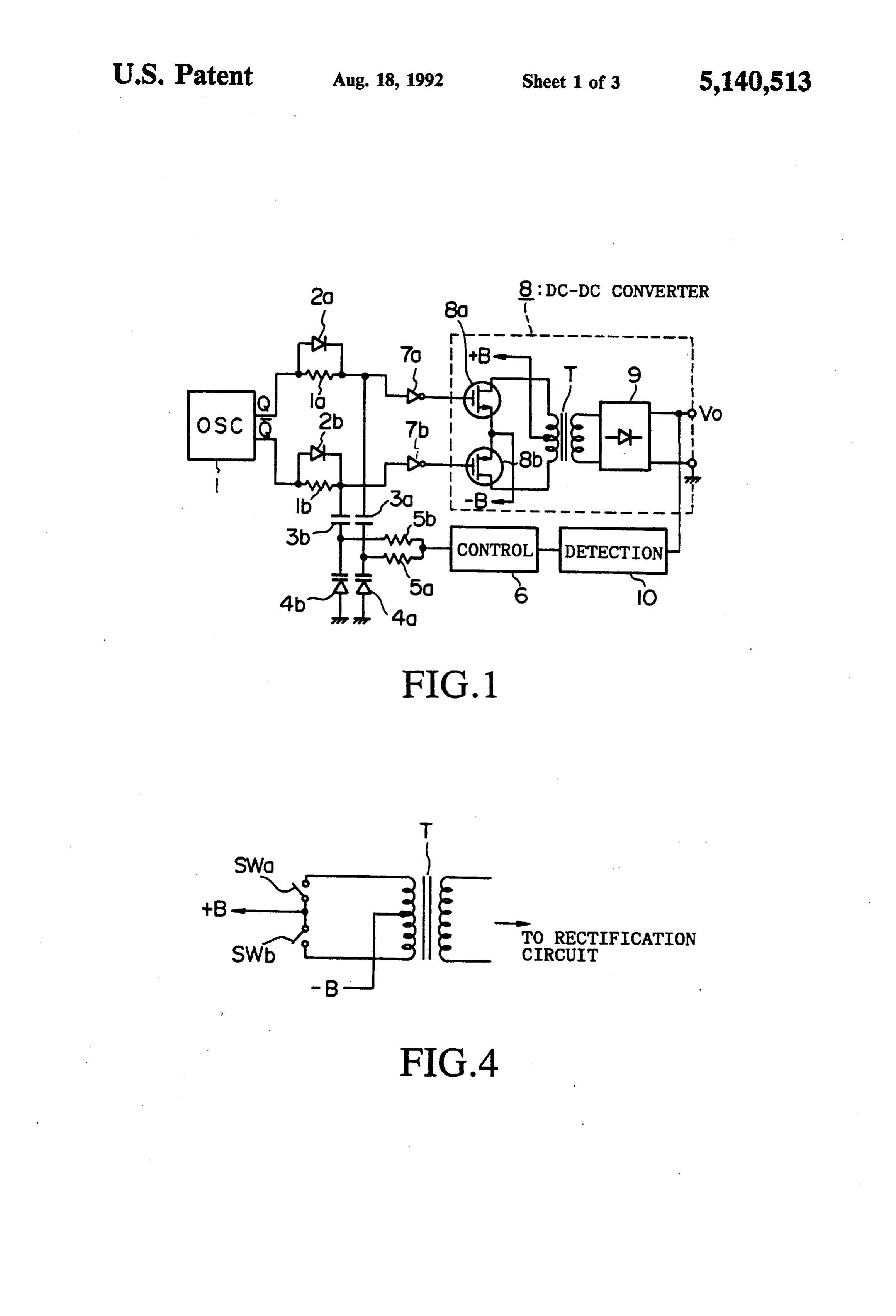
Q OF OSCILLATOR 1
Q OF OSCILLATOR 1
OF INVERTER 7a
OUTPUT SIGNAL
OF INVERTER 7a
OF INVERTER 7b
OUTPUT SIGNAL
OF INVERTER 7b
PRIMARY VOLTAGE
OF TRANSFORMER T1
Page 4
Drawing sheet — no readable text.
Page 5
of oscillation frequency of oscillators is low, and the
SWITCHING REGULATED DC-DC CONVERTER oscillation frequency restricts the switching frequency USING WARIABLE CAPACTY DODES IN THE of switching regulated power supplies to a range of FEEDBACK CIRCUIT approximately 10 kHz up to 100 kHz. In addition, the bi-polar transistor IC consumes a large amount of elec
BACKGROUND OF THE INVENTION tric power. Furthermore, the configuration of the cir 1. Field of the Invention cuit of the specificated bi-polar transistor IC is compli The present invention relates to a switching regulated cated and therefore costly.
power supply, the output voltage of which is regulated O SUMMARY OF THE INVENTION by a pulse width modulation method.
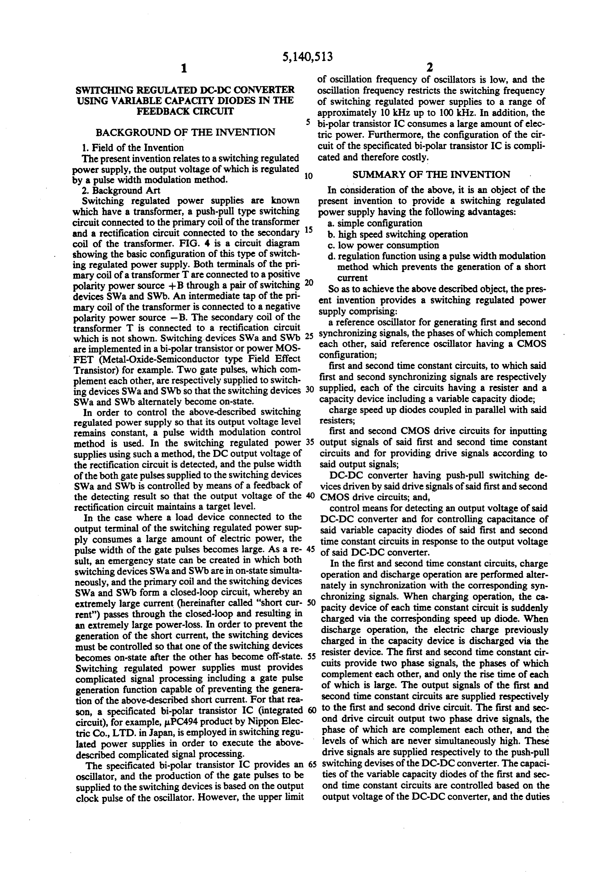
2. Background Art In consideration of the above, it is an object of the Switching regulated power supplies are known present invention to provide a switching regulated which have a transformer, a push-pull type switching power supply having the following advantages: circuit connected to the primary coil of the transformer 15 a. simple configuration and a rectification circuit connected to the secondary b. high speed switching operation coil of the transformer. FIG. 4 is a circuit diagram c. low power consumption showing the basic configuration of this type of switch d, regulation function using a pulse width modulation ing regulated power supply. Both terminals of the pri method which prevents the generation of a short mary coil of a transformer T are connected to a positive creat polarity power source +B through a pair of switching So as to achieve the above described object, the pres devices SWa and SWb. An intermediate tap of the pri ent invention provides a switching regulated power mary coil of the transformer is connected to a negative supply comprising:
polarity power source -B. The secondary coil of the a reference oscillator for generating first and second transformer T is connected to a rectification circuit 25 synchronizing signals, the phases of which complement which is not shown. Switching devices SWa and SWb each other, said are implemented in a bi-polar transistor or power MOS configuration; reference oscillator having a CMOS FET (Metal-Oxide-Semiconductor type Field Effect
Transistor) for example. Two gate pulses, which com firstfirstandandsecond second time constant circuits, to which said plement each other, are respectively supplied to switch 30 supplied, each ofsynchronizing the circuits signals are respectively having a resister and a ing devices SWa and SWb so that the switching devices capacity device including a variable capacity diode; SWa and SWb alternately become on-state.
In order to control the above-described switching charge speed up diodes coupled in parallel with said regulated power supply so that its output voltage level resisters;
remains constant, a pulse width modulation control first and second CMOS drive circuits for inputting method is used. In the switching regulated power 35 output signals of said first and second time constant supplies using such a method, the DC output voltage of circuits and for providing drive signals according to the rectification circuit is detected, and the pulse width said output signals;
of the both gate pulses supplied to the switching devices DC-DC converter having push-pull switching de SWa and SWb is controlled by means of a feedback of vices driven by said drive signals of said first and second the detecting result so that the output voltage of the 40 CMOS drive circuits; and, rectification circuit maintains a target level. control means for detecting an output voltage of said In the case where a load device connected to the DC-DC converter and for controlling capacitance of output terminal of the switching regulated power sup said variable capacity diodes of said first and second ply consumes a large amount of electric power, the 45 time constant circuits in response to the output voltage pulse width of the gate pulses becomes large. As a re of said DC-DC converter.
sult, an emergency state can be created in which both In the first and second time constant circuits, charge switching devices SWa and SWb are in on-state simulta operation and discharge operation are performed alter neously, and the primary coil and the switching devices nately in synchronization with the corresponding syn SWa and SWb form a closed-loop circuit, whereby an chronizing signals. When charging operation, the ca extremely large current (hereinafter called "short cur 50 pacity device of each time constant circuit is suddenly rent") passes through the closed-loop and resulting in charged via the corresponding speed up diode. When an extremely large power-loss. In order to prevent the discharge generation of the short current, the switching devices charged inoperation, the the electric charge previously capacity device is discharged via the must be controlled so that one of the switching devices resister device. The first and second time constant cir becomes on-state after the other has become off-state. cuits provide two phase signals,
the phases of which
Switching regulated power supplies must provides complicated signal processing including a gate pulse complement each other, and only the rise time of each of which is large. The output signals of the first and generation function capable of preventing the genera second time constant circuits are supplied respectively tion of the above-described short current. For that rea son, a specificated bi-polar transistor IC (integrated to the first and second drive circuit. The first and sec circuit), for example, PC494 product by Nippon Elec ond drive circuit output two phase drive signals, the tric Co., LTD. in Japan, is employed in switching regul phase of which are complement each other, and the lated power supplies in order to execute the above drive levels of which are never simultaneously high. These described complicated signal processing. signals are supplied respectively to the push-pull The specificated bi-polar transistor IC provides an 65 switching devises of the DC-DC converter. The capaci oscillator, and the production of the gate pulses to be ties of the variable capacity diodes of the first and sec supplied to the switching devices is based on the output ond time constant circuits are controlled based on the clock pulse of the oscillator. However, the upper limit output voltage of the DC-DC converter, and the duties
Page 6
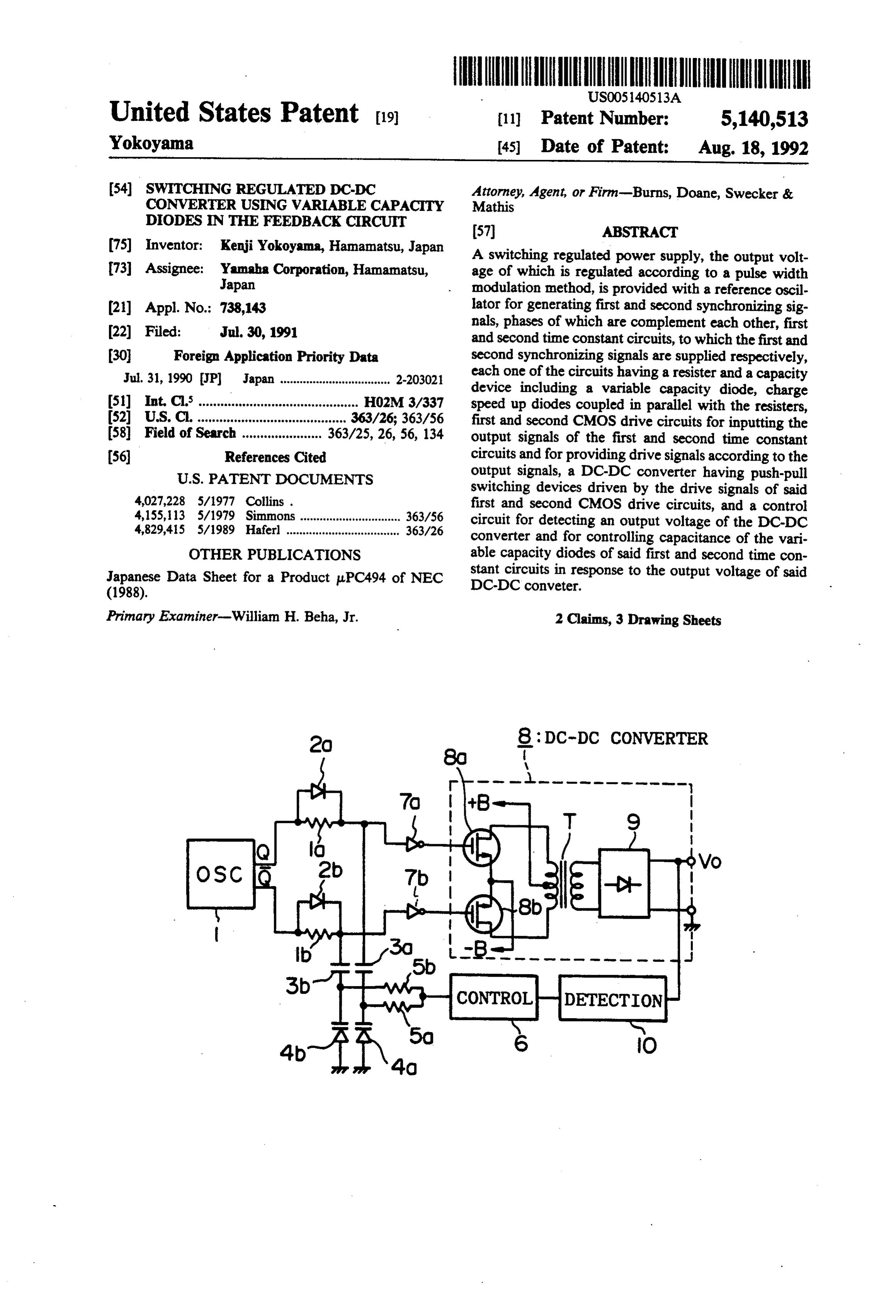
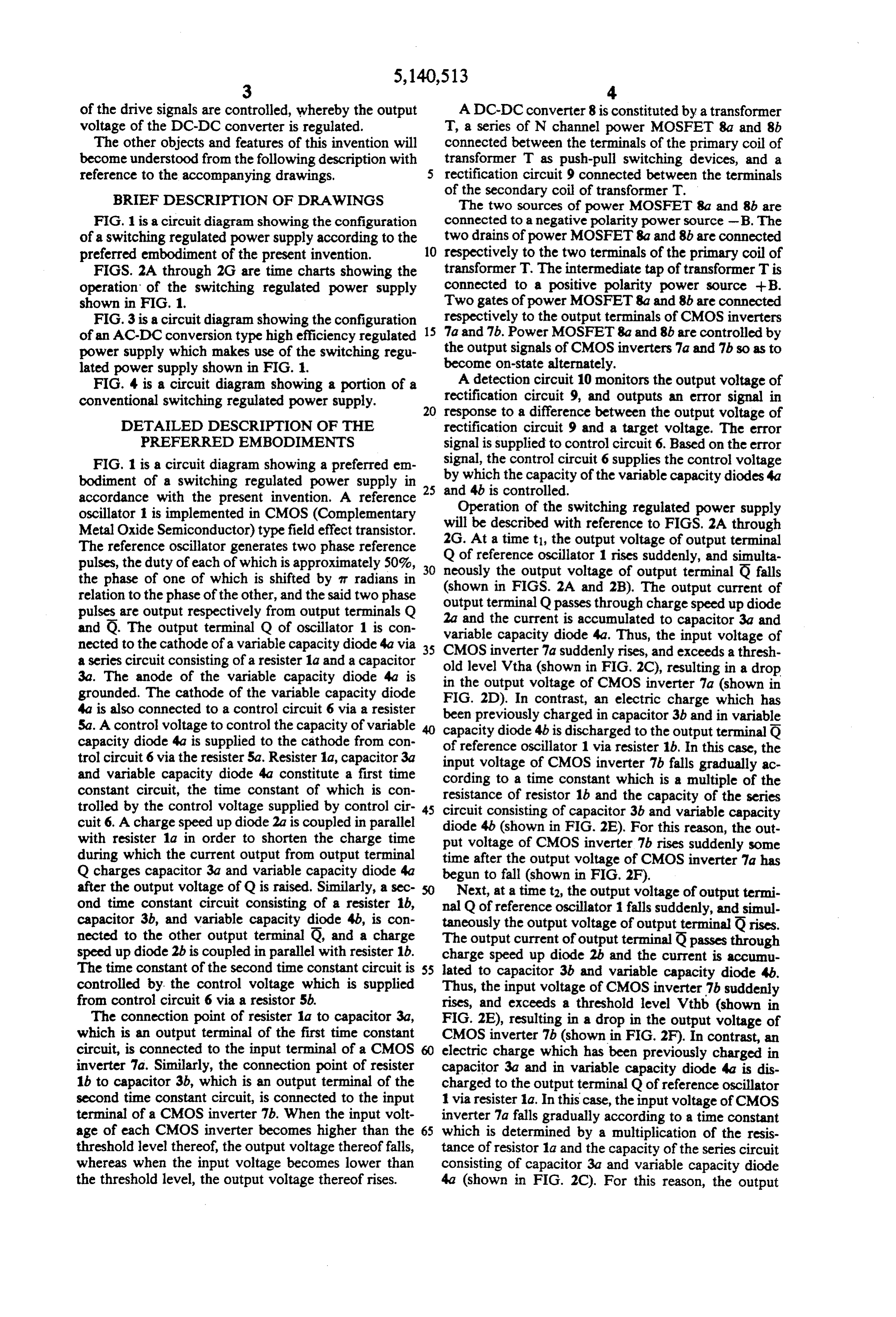
of the drive signals are controlled, whereby the output A DC-DC converter 8 is constituted by a transformer voltage of the DC-DC converter is regulated. T, a series of N channel power MOSFET 8a and 8b The other objects and features of this invention will connected between the terminals of the primary coil of become understood from the following description with transformer T as push-pull switching devices, and a reference to the accompanying drawings. rectification circuit 9 connected between the terminals
BRIEF DESCRIPTION OF DRAWINGS
of the secondary coil of transformer T.
The two sources of power MOSFET 8a and 8b are
FIG. 1 is a circuit diagram showing the configuration connected to a negative polarity power source -B. The of a switching regulated power supply according to the two drains of power MOSFET 8a and 8b are connected preferred embodiment of the present invention. O respectively to the two terminals of the primary coil of FIGS. 2A through 2G are time charts showing the transformer T. The intermediate tap of transformer T is operation of the switching regulated power supply connected to a positive polarity power source --B. shown in FIG. 1. Two gates of power MOSFET 8a and 8b are connected FIG. 3 is a circuit diagram showing the configuration respectively to the output terminals of CMOS inverters of an AC-DC conversion type high efficiency regulated 15 7a and 7b. Power MOSFET 8a and 8b are controlled by power supply which makes use of the switching regu the output signals of CMOS inverters 7a and 7b so as to lated power supply shown in FIG. 1. become on-state alternately.
FIG. 4 is a circuit diagram showing a portion of a A detection circuit 10 monitors the output voltage of conventional switching regulated power supply. rectification circuit 9, and outputs an error signal in 20 response to a difference between the output voltage of
DETAILED DESCRIPTION OF THE rectification circuit 9 and a target voltage. The error PREFERRED EMBODIMENTS signal is supplied to control circuit 6. Based on the error FIG. 1 is a circuit diagram showing a preferred em signal, the control circuit 6 supplies the control voltage bodiment of a switching regulated power supply in 25 by which the capacity of the variable capacity diodes 4a accordance with the present invention. A reference andOperation 4b is controlled.
of the switching regulated power supply oscillator 1 is implemented in CMOS (Complementary will be described with reference to FIGS. 2A through Metal Oxide Semiconductor) type field effect transistor. 2G. At a time t1, the output voltage of output terminal The reference oscillator generates two phase reference Q of reference oscillator 1 rises suddenly, and simulta pulses, the duty of each of which is approximately 50%, 30 neously the output voltage of output terminal Q falls the phase of one of which is shifted by at radians in (shown in FIGS. 2A and 2B). The output current of relation to the phase of the other, and the said two phase pulses are output respectively from output terminals Q output terminal Qpasses through charge speed up diode and Q. The output terminal Q of oscillator 1 is con 2a and the current is accumulated to capacitor 3a and variable capacity diode 4a. Thus, the input voltage of nected to the cathode of a variable capacity diode 4a via 35 CMOS inverter 7a suddenly rises, and exceeds a thresh a series circuit consisting of a resister 1a and a capacitor old level Vitha (shown 3a. The anode of the variable capacity diode 4a is in the output voltage ofinCMOS FIG. 2C), resulting in a drop inverter 7a (shown in grounded. The cathode of the variable capacity diode FIG. 2D). In contrast, an electric 4a is also connected to a control circuit 6 via a resister been previously charged in capacitorcharge which has 3b and in variable 5a. A control voltage to control the capacity of variable capacity diode 4b is discharged to the output terminal Q capacity diode 4a is supplied to the cathode from con of reference oscillator 1 via resister b. In this case, the trol circuit 6 via the resister 5a. Resister 1a, capacitor 3a input voltage of CMOS inverter 7b falls gradually ac and variable capacity diode 4a constitute a first time cording to a time constant which is a multiple of the constant circuit, the time constant of which is con resistance of resistor 1b and the capacity of the series trolled by the control voltage supplied by control cir 45 circuit cuit 6. A charge speed up diode 2a is coupled in parallel diode 4bconsisting of capacitor 3b and variable capacity (shown in FIG. 2E). For this reason, the out with resister 1a in order to shorten the charge time put voltage of CMOS inverter 7b rises suddenly some during which the current output from output terminal time after the output voltage of CMOS inverter 7a has Q charges capacitor 3a and variable capacity diode 4a begun to fall (shown in FIG. 2F).
after the output voltage of Q is raised. Similarly, a sec Next, at a time t2, the output voltage of output termi ond time constant circuit consisting of a resister 1b, mal Q of reference oscillator 1 falls suddenly, and simul capacitor 3b, and variable capacity diode 4b, is con taneously the output voltage of output terminal Q rises. nected to the other output terminal Q, and a charge The output current of output terminal Qpasses through speed up diode 2b is coupled in parallel with resister 1b. charge speed up diode 2b and the current is accumu The time constant of the second time constant circuit is 55 lated to capacitor 3b and variable capacity diode 4b. controlled by the control voltage which is supplied Thus, the input voltage of CMOS inverter 7b suddenly from control circuit 6 via a resistor 5b. rises, and exceeds a threshold level Vthb (shown in The connection point of resister 1a to capacitor 3a, FIG. 2E), resulting in a drop in the output voltage of which is an output terminal of the first time constant CMOS inverter 7b (shown in FIG.2F). In contrast, an circuit, is connected to the input terminal of a CMOS electric charge which has been previously charged in inverter 7a. Similarly, the connection point of resister capacitor 3a and in variable capacity diode 4a is dis 1b to capacitor 3b, which is an output terminal of the charged to the output terminal Q of reference oscillator second time constant circuit, is connected to the input 1 via resister 1a. In this case, the input voltage of CMOS terminal of a CMOS inverter 7b. When the input volt inverter 7a falls gradually according to a time constant age of each CMOS inverter becomes higher than the 65 which is determined by a multiplication of the resis threshold level thereof, the output voltage thereof falls, tance of resistoria and the capacity of the series circuit whereas when the input voltage becomes lower than consisting of capacitor 3a and variable capacity diode the threshold level, the output voltage thereof rises. 4a (shown in FIG. 2C). For this reason, the output
Page 7
voltage of CMOS inverter 7a rises when a few time MOS devices. Thus, standard MOS devices having high elapses after the output voltage of CMOS inverter 7b speed, which can be used for reference oscillator 1, has fallen (shown in FIG. 2D). inverters 7a and 7b, power MOSFET 8a and 8b, can be In this manner, two phase pulses, the phases of which obtained. By employing these high speed standard de complement each other, and the levels of which are vices, a high performance switching regulated power never simultaneously high, are output respectively from supply capable of high speed switching operation can CMOS inverters 7a and 7b, and the said two phase be produced at low cost.
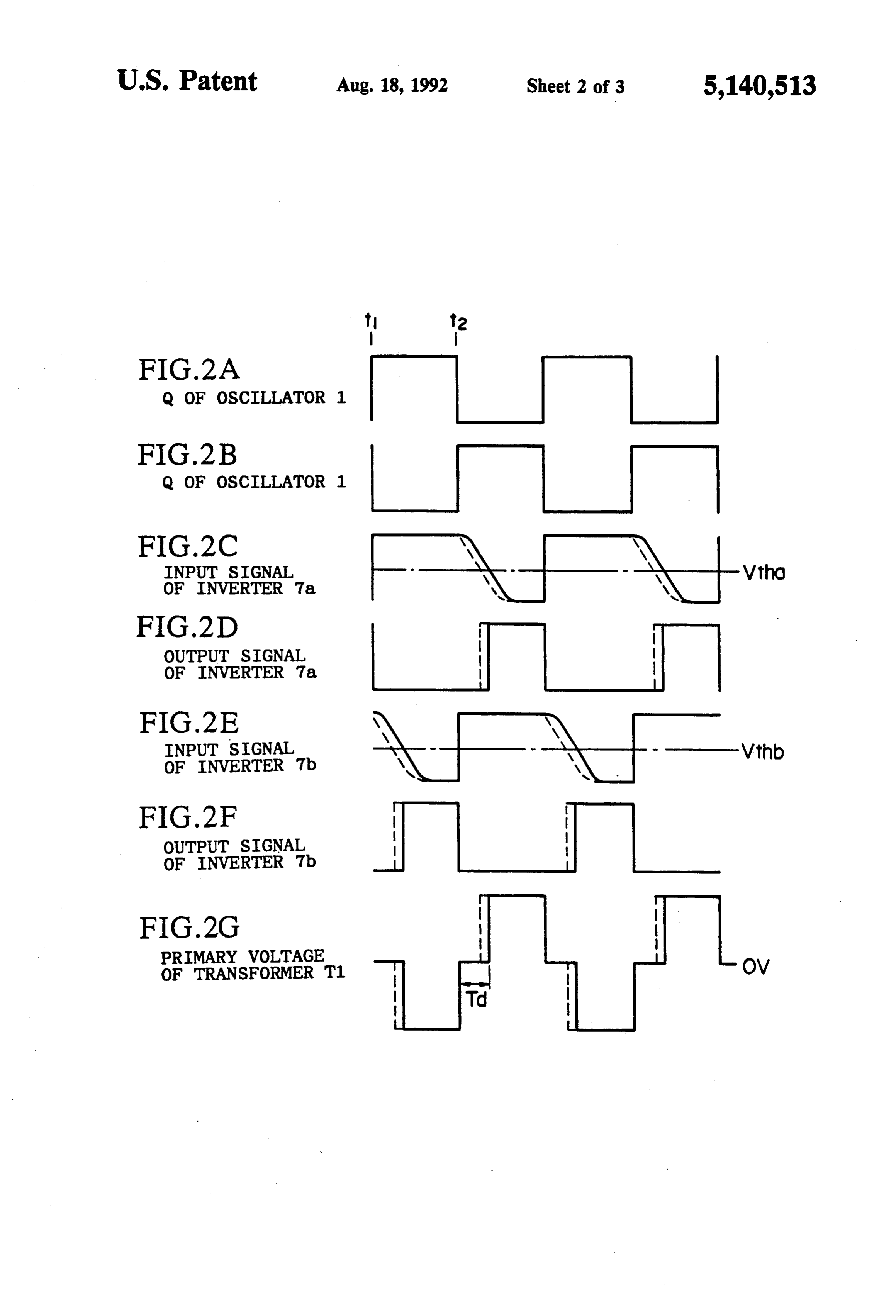
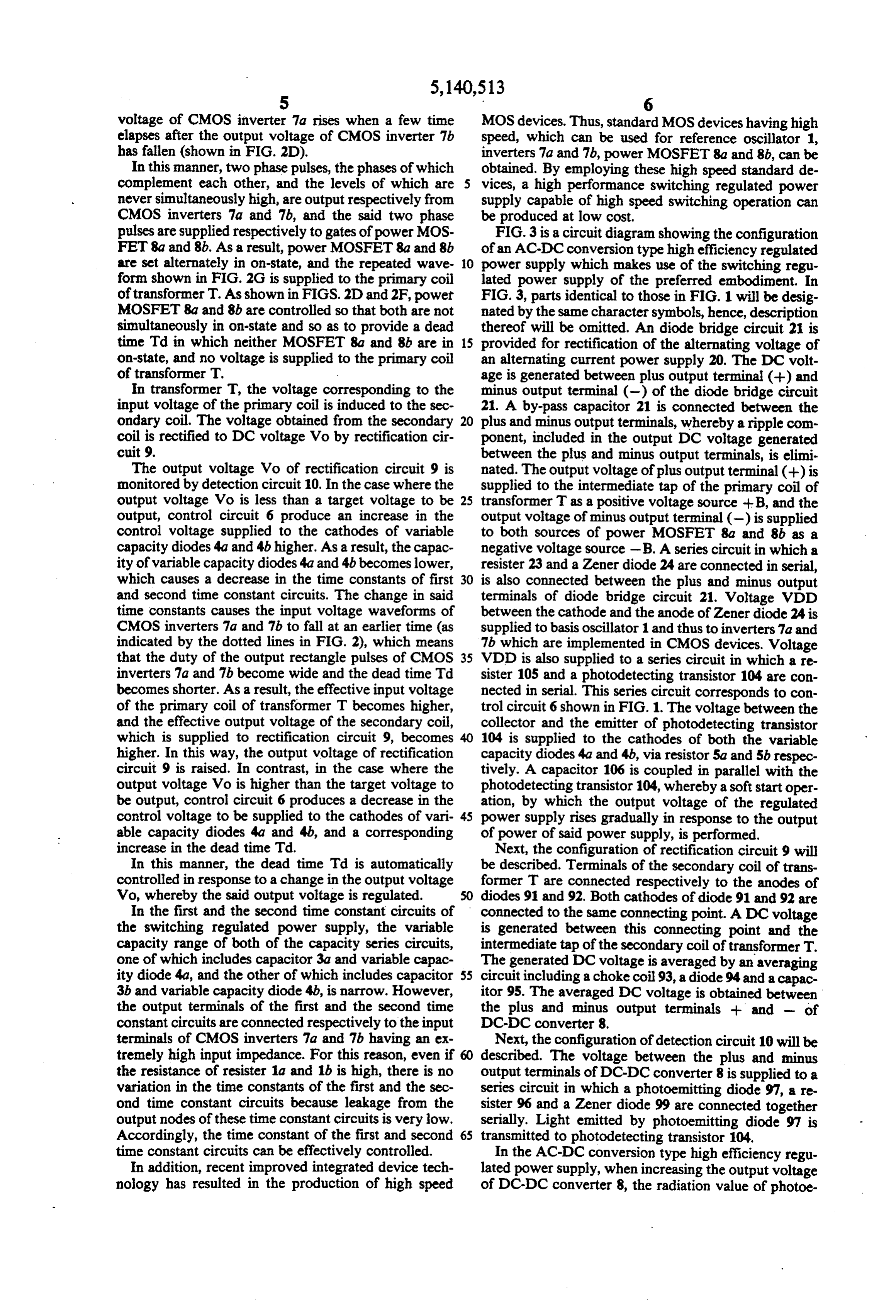
pulses are supplied respectively to gates of power MOS FIG.3 is a circuit diagram showing the configuration FET 8a and 8b. As a result, power MOSFET 8a and 8b of an AC-DC conversion type high efficiency regulated are set alternately in on-state, and the repeated wave 0 power supply which makes use of the switching regu form shown in FIG. 2G is supplied to the primary coil lated power supply of the preferred embodiment. In of transformer T. As shown in FIGS. 2D and 2F, power FIG. 3, parts identical to those in FIG. 1 will be desig MOSFET 8a and 8b are controlled so that both are not nated by the same character symbols, hence, description simultaneously in on-state and so as to provide a dead thereof will be omitted. An diode bridge circuit 21 is time Tod in which neither MOSFET 8a and 8b are in 15 provided for rectification of the alternating voltage of on-state, and no voltage is supplied to the primary coil an alternating current power supply 20. The DC volt of transformer T. age is generated between plus output terminal (--) and In transformer T, the voltage corresponding to the minus output terminal (-) of the diode bridge circuit input voltage of the primary coil is induced to the sec 21. A by-pass capacitor 21 is connected between the ondary coil. The voltage obtained from the secondary 20 plus and minus output terminals, whereby a ripple com coil is rectified to DC voltage Vo by rectification cir ponent, included in the output DC voltage generated cuit 9. between the plus and minus output terminals, is elimi The output voltage Vo of rectification circuit 9 is nated. The output voltage of plus output terminal (--) is monitored by detection circuit 10. In the case where the supplied to the intermediate tap of the primary coil of output voltage Vo is less than a target voltage to be 25 transformer T as a positive voltage source --B, and the output, control circuit 6 produce an increase in the output voltage of minus output terminal (-) is supplied control voltage supplied to the cathodes of variable to both sources of power MOSFET 8a and 8b as a capacity diodes 4a and 4b higher. As a result, the capac negative voltage source - B. A series circuit in which a ity of variable capacity diodes 4a and 4b becomes lower, resister 23 and a Zener diode 24 are connected in serial, which causes a decrease in the time constants of first 30 is also connected between the plus and minus output and second time constant circuits. The change in said terminals of diode bridge circuit 21. Voltage VDD time constants causes the input voltage waveforms of between the cathode and the anode of Zener diode 24 is CMOS inverters 7a and 7b to fall at an earlier time (as supplied to basis oscillator 1 and thus to inverters 7a and indicated by the dotted lines in FIG. 2), which means 7b which are implemented in CMOS devices. Voltage that the duty of the output rectangle pulses of CMOS 35 VDD is also supplied to a series circuit in which a re inverters 7a and 7b become wide and the dead time Tod sister 105 and a photodetecting transistor 104 are con becomes shorter. As a result, the effective input voltage nected in serial. This series circuit corresponds to con of the primary coil of transformer T becomes higher, trol circuit 6 shown in FIG.1. The voltage between the and the effective output voltage of the secondary coil, collector and the emitter of photodetecting transistor which is supplied to rectification circuit 9, becomes 104 is supplied to the cathodes of both the variable higher. In this way, the output voltage of rectification capacity diodes 4a and 4b, via resistor 5a and 5b respec circuit 9 is raised. In contrast, in the case where the tively. A capacitor 106 is coupled in parallel with the output voltage Vo is higher than the target voltage to photodetecting transistor 104, whereby a soft start oper be output, control circuit 6 produces a decrease in the ation, by which the output voltage of the regulated control voltage to be supplied to the cathodes of vari 45 power supply rises gradually in response to the output able capacity diodes 4a and 4b, and a corresponding of power of said power supply, is performed. increase in the dead time Td. Next, the configuration of rectification circuit 9 will In this manner, the dead time Tod is automatically be described. Terminals of the secondary coil of trans controlled in response to a change in the output voltage former T are connected respectively to the anodes of Vo, whereby the said output voltage is regulated. 50 diodes 91 and 92. Both cathodes of diode 91 and 92 are In the first and the second time constant circuits of connected to the same connecting point. A DC voltage the switching regulated power supply, the variable is generated between this connecting point and the capacity range of both of the capacity series circuits, intermediate tap of the secondary coil of transformer T. one of which includes capacitor 3a and variable capac The generated DC voltage is averaged by an averaging ity diode 4a, and the other of which includes capacitor 55 circuit including a choke coil 93, a diode 94 and a capac 3b and variable capacity diode 4b, is narrow. However, itor 95. The averaged DC voltage is obtained between the output terminals of the first and the second time the plus and minus output terminals + and - of constant circuits are connected respectively to the input DC-DC converter 8.
terminals of CMOS inverters 7a and 7b having an ex Next, the configuration of detection circuit 10 will be tremely high input impedance. For this reason, even if 60 described. The voltage between the plus and minus the resistance of resister 1a and 1b is high, there is no output terminals of DC-DC converter 8 is supplied to a variation in the time constants of the first and the sec series circuit in which a photoemitting diode 97, a re ond time constant circuits because leakage from the sister 96 and a Zener diode 99 are connected together output nodes of these time constant circuits is very low. serially. Light emitted by photoemitting diode 97 is Accordingly, the time constant of the first and second 65 transmitted to photodetecting transistor 104. time constant circuits can be effectively controlled. In the AC-DC conversion type high efficiency regu In addition, recent improved integrated device tech lated power supply, when increasing the output voltage nology has resulted in the production of high speed of DC-DC converter 8, the radiation value of photoe
Page 8
mitting diode 97 increases. As a result, the resistance charge speed up diodes coupled in parallel with said between the collector and the emitter of photodetecting resisters;
transistor 104 decreases, whereby the voltage supplied first and second CMOS drive circuits for inputting to variable capacity diode 4a and 4b decreases. Accord output signals of said first and second time constant ingly, the time constants of the first and second time circuits, and for providing drive signals according constant circuits increase and the dead time Tod is ex to said output signals;
tended. In contrast, when decreasing the output voltage a DC-DC converter having push-pull switching de of DC-DC converter 8, the radiation value of photoe vices driven by said drive signals of said first and second CMOS drive circuits; and, mitting diode 97 decreases. As a result, the resistance 10 a control between the collector and the emitter of photodetecting means for detecting an output voltage of transistor 104 increases, whereby the voltage supplied said DC-DC converter and for controlling capaci to variable capacity diode 4a and 4b increases. Accord tance of said variable capacity diodes of said first ingly, the time constants of the first and second time and second time constant circuits in response to constant circuits decrease and the dead time Td is short 15 2. said
output voltage of said DC-DC converter.
switching regulated power supply according to ened. In this manner, the output voltage is regulated. claim 1 wherein said control means includes: What is claimed is: a detection circuit for generating a optical signal 1. A switching regulated power supply comprising: which indicates the change of said output voltage a reference oscillator for generating first and second of said DC-DC converter; and synchronizing signals, phases of which are comple 20 a control circuit having a series circuit consisting of a ment each other, said reference oscillator having a resister and a photodetecting transistor which ac CMOS configuration; cepts said optical signal, and where the voltage at first and second time constant circuits, to which said the connecting point between said resister and said first and second synchronizing signals are supplied photodetecting transistor is supplied to said vari respectively, each one of the circuits having a re 25 able capacity diodes so that the capacitance of said sister and a capacity device including a variable variable capacity diodes is controlled. capacity diode; se s
Provenance
- Collection
- Cited prior art
- Original PDF
- patentimages.storage.googleapis.com →
- Filed
- 1991-07-30
- Pages
- 8
- Method
- pdftotext (the PDF's own text layer) + pdftoppm 300dpi page scans
- Source
- Google Patents bibliographic record
- Granted
- 1992-08-18
- Inventors
- Kenji Yokoyama; Yamaha Corp
- Transcribed from
- patentimages.storage.googleapis.com →