patent · US5131954
Monolithic solar cell array and method for its manufacturing
21 July 1992
Page 1 — bibliographic record
United States Patent (19) (11 Patent Number: 5,131,954 Vogeli et al. (45) Date of Patent: Jul. 21, 1992 54) MONOLITHIC SOLAR CELL ARRAY AND 4.670.294 6/1987 Yamazaki ........................... 427/53.1 METHOD FOR ITS MANUFACTURING 4,754,544 7/1988 Hanak ..................................... 437/2 4.758,526 7/1988 Thalheimer ............................. 437/2 (75) Inventors: Craig Vogeli, New Baltimore; Prem 4,773,943 9/1988 Yamaguchi et al ... 136/244 Nath, Rochester Hills, both of Mich. 4,824,488 4/1989 Sakai et al. .......................... 36/244 4,956,023 9/1990 Tsuge et al. ........................ 136/244 (73) Assignee: United Solar Systems Corporation, FOREIGN PATENT DOCUMENTS Troy, Mich.
21 Appl. No.: 798,848 1-93174 4/1989 Japan ................................... 36/244 1-152769 6/1989 Japan ................ - - - - - - - - - - - - - - - - - 136/244
Primary Examiner-Aaron Weisstuch
Related U.S. Application Data Attorney, Agent, or Firm-Krass & Young 63) Continuation of Ser. No. 597,407, Oct. 15, 1990, aban (57) ABSTRACT doned.
Large area, thin-film body of photovoltaic material is (51) Int. Cl. ...................... H01L 31/05; H01L 31/08 subdivided into a plurality of small area devices. (52) U.S. Cl. ........................................ 136/244; 437/2; Through a selective etching process, a portion of the 437/4; 437/205 botton electrode of each small area device is exposed.
58 Field of Search ........................................ 437/2-5, A metallic contact member is deposited upon the ex 437/205; 136/244 posed portion of the electrode and a series connection (56) References Cited between adjoining cells is established by interconnect
top electrode of an adjoining cell, so as to provide a 4,243.432 l/1981 Jordan et al. ....................... 36/244 large-area photovoltaic device including a plurality of 4,315.096 2/1982 Tyan et al. ....... ... 36/244 interconnected sub-cells.
4,419,533 12/1983 Czubaty et al. . ... 136/259 4,514.579 4/1985 Hanak ....... ... 36/249 4.594,471 6/1986 Yamazaki ............................ 136/249 18 Claims, 4 Drawing Sheets
Page 2
Drawing sheet — no readable text.
Page 3
Drawing sheet — no readable text.
Page 4
Drawing sheet — no readable text.
Page 5
Drawing sheet — no readable text.
Page 6
Techniques for the manufacture of monolithic arrays
MONOLITHIC SOLAR CELL ARRAY AND of photovoltaic devices have been implemented in the METHOD FOR ITS MANUFACTURING prior art and such techniques typically involve the use of etching, scribing or similar techniques for subdivid
This is a continuation of co-pending application Ser. 5 ing semiconductor layers into discrete, electrically iso No. 597,407 filed on Oct. 15, 1990, now abandoned. lated portions and employ subsequent steps for deposit FIELD OF THE INVENTION ing additional semiconductor layers and for intercon necting these portions. Prior art techniques generally
This invention relates generally to large area arrays involve scribing a device into small area cells which are of interconnected photovoltaic devices and more par O connected in a top to bottom relationship. These tech ticularly to a large area array comprised of a plurality of niques necessitate alternating vacuum deposition tech smaller area cells disposed in an interconnected rela niques with scribing or wet-etching or plasma etching tionship upon a single substrate, as well as to methods steps. The repeated steps of vacuum deposition and for the manufacture of the array. atmospheric processing contaminate both the deposi 15 tion apparatus and the devices, thus reducing the qual
BACKGROUND OF THE INVENTION
ity of the devices and the efficiency of the process.
Photovoltaic power represents a non-depletable re In typical prior art techniques, contact between the source which is globally available and non polluting. isolated subcells is generally made between relatively Because of the increasing scarcity of non-renewable large area portions of adjoining cells. The reason for the energy sources such as coal, petroleum and uranium 20 large area contact is two fold. Generally, the subcells and the ever-increasing problems attendant upon their are fairly small and a large contact area is utilized to use, it is essential that greater use be made of solar en accommodate various inaccuracies of the screen print ergy.
Single crystal photovoltaic devices, especially crys ing or lithographic process utilized for interconnection; also, contact is generally made through the use of print talline silicon photovoltaic devices have been utilized able materials
for some time as sources of electrical power. However, inks and these such as electrically conductive paste or materials typically manifest a fairly high the utility of such crystalline devices has been limited contact resistance; consequently, by problems associated with the manufacture thereof. utilized to enable full withdrawala large area must be of photogenerated
More particularly, single crystalline materials are diffi power. This large contact area represents a loss of ac cult to produce in sizes substantially larger than several 30 inches in diameter, relatively fragile, relatively thick, tive cell surface. U.S. Pat. No. 4,315,096 of Tyan et al. and heavy; furthermore, they are expensive and time discloses a technique for fabrication of an array of pho consuming to fabricate. Recently, considerable effort tovoltaic devices, which technique utilizes a contact has been expended to develop systems and processes for region extending across the width, and a substantial preparing thin film semiconductor alloy materials 35 portion of the length, of the subcells of the device. which encompass relatively large areas and which can Other techniques for the fabrication of interconnected be deposited so as to form doped semiconductor layers arrays are disclosed in U.S. Pat. No. 4,754,544. for the production of thin film photovoltaic devices The preparation of most thin film photovoltaic de which are substantially equivalent, or superior, to their vices involves depositing various semiconductor layers crystalline counterparts in operation and efficiency. by at least one vacuum step employing a process such as Such materials are disclosed in U.S. Pat. Nos. 4,226,898 evaporation, sputtering or glow discharge deposition. and 4,217,374 of Ovshinsky et al. It is now possible to The presence of volatile species on the device or sub deposit high quality, thin film semiconductor alloy ma strate can contaminate the interior of a vacuum deposi terials over large areas in a roll-to-roll process so as to tion apparatus and degrade the semiconductor layers. enable the fabrication of large area devices. Such tech 45 Many prior art techniques for the preparation of mono niques are disclosed in U.S. Pat. Nos. 4,410,558 and lithic photovoltaic devices require vacuum deposition 4,485,125. Such large area deposition techniques offer of semiconductors to be carried out on a device which the advantage of high speed and economy. Generally, it has previously been subjected to wet etching, solvent is desirable to subdivide a large area photovoltaic de based coating or other such techniques which can leave vice into a plurality of smaller area devices which are 50 a residue of volatile contaminants thereupon. Since interconnected in series and/or parallel arrays to pro prior art techniques require intermingled deposition and vide a desired level of voltage and power. etching steps, the semiconductor deposition cannot be Subdivision and interconnection of a large area de separated from the array fabrication. It is not possible to vice may be carried out by severing the large area de employ a "generic' photovoltaic body which is amena vice into a plurality of discrete devices which are then 55 ble to various processing techniques. It clearly would interconnected to form a module. This technique is be desirable to have a method for manufacturing a quite labor intensive and more practical for forming monolithic photovoltaic device which separates the modules from a relatively smaller number of large de semiconductor deposition steps from the wet processing vices. However, it is impractical for interconnecting a steps.
large number of small area devices. Another approach Prior art interconnection techniques also tend to give to the task of interconnecting small area devices in a high series resistance array. The interconnections volves the manufacture of monolithic devices. As uti between the cells often rely upon the use of materials lized within the context of the present invention, the which alloy with the various cell components to create term "monolithic' defines an interconnected array a high resistance contact. In other instances, the pro formed fron a body of semiconductor material which is 65 cessing techniques oxidize or otherwise degrade the disposed upon a single large area substrate; in contrast contacts. It is therefore desirable to interconnect small to the discrete cell approach, fabricating a monolithic area subcells by a technique which avoids oxidation or device involves no severing of the substrate. alloying and thereby provides a low resistance contact.
Page 7
The present invention provides an improved mono present invention consists of a relatively thick support lithic photovoltaic device comprised of a plurality of layer 11a and a flexible, relatively thin insulating layer interconnected small area subcells disposed upon a sin 11b, both of which will be described in greater detail . gle, large area substrate. The connections between the hereinbelow.
cells are made through the use of materials which retain An electrically conductive bottom electrode layer 17 high conductivity. Thus, contact areas can be made is operatively disposed atop the insulating layer 11b so small. The small contact area also provides increased as to be in electrical communication with the semicon active cell area and hence high photo conversion effi ductor cells 12a, 2b, 12c formed thereatop. It is to be ciencies. The device of the present invention is manu noted at this point that in some cases it is desirable to factured by a process which segregates the semiconduc 10 include a relatively transparent, preferably textured, tor deposition and wet processing steps so as to avoid layer disposed between the bottom electrode layer 17 problems of contamination and to speed up process and the semiconductor body, in this instance the cells time. These and other advantages of the present inven 12a, 12b, 12c. This layer which will be described in tion will be readily apparent from the drawings, discus greater detail with regard to FIG. 3b serves to scatter sion and description which follow. 15 and redirect light passing through the cell and therefore
BRIEF DESCRIPTION OF THE DRAWINGS
increase cell efficiency. It is to be understood that the present invention may be practiced with or without
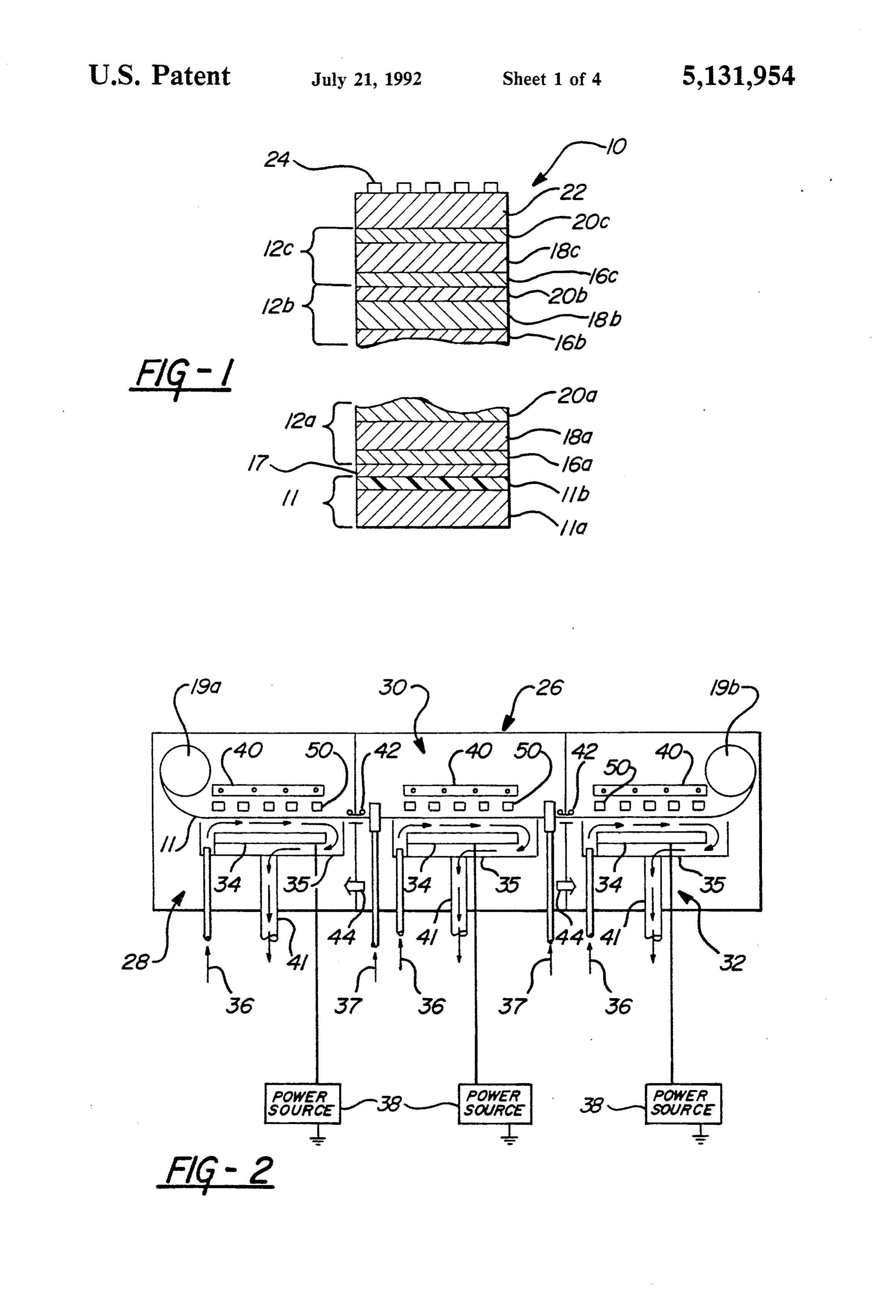
FIG. 1 is a fragmentary, cross-sectional view of a thin such a layer.
film tandem photovoltaic device typical of those which Each of the cells 12a, 2b and 12c, in this embodi may comprise the subcells of the monolithic array of the 20 ment, are fabricated with an amorphous semiconductor present invention; body containing at least one layer of a silicon or germa FIG. 2 is a diagrammatic representation of a multiple nium alloy material. Each of the semiconductor bodies chamber, glow discharge deposition system adapted for includes an n-type conductivity layer 20a, 20b and 20c. the continuous production of photovoltaic devices of an intrinsic layer 18a, 18b and 18c, and a p-type conduc the type shown in FIG. 1; 25 tivity layer 16a, 16b and 16c. As illustrated, cell 12b is an FIG. 3A is a top plan view of a portion of a large area intermediate cell and as indicated in FIG. 1, additional photovoltaic device prior to subdividing; intermediate cells may be stacked atop cells without FIG. 3B is a cross-sectional view of the large area departing from the spirit or scope of the present inven device of FIG. 3A; tion. Also, although P-I-N cells are illustrated the pres FIG. 4A is a top plan view of the device of FIG. 3A 30 ent invention may be implemented with N-I-P cells as at a first step of processing: well as cells of other configurations such as schottky FIG. 4B is a cross-sectional view of a portion of the barrier diodes and the like.
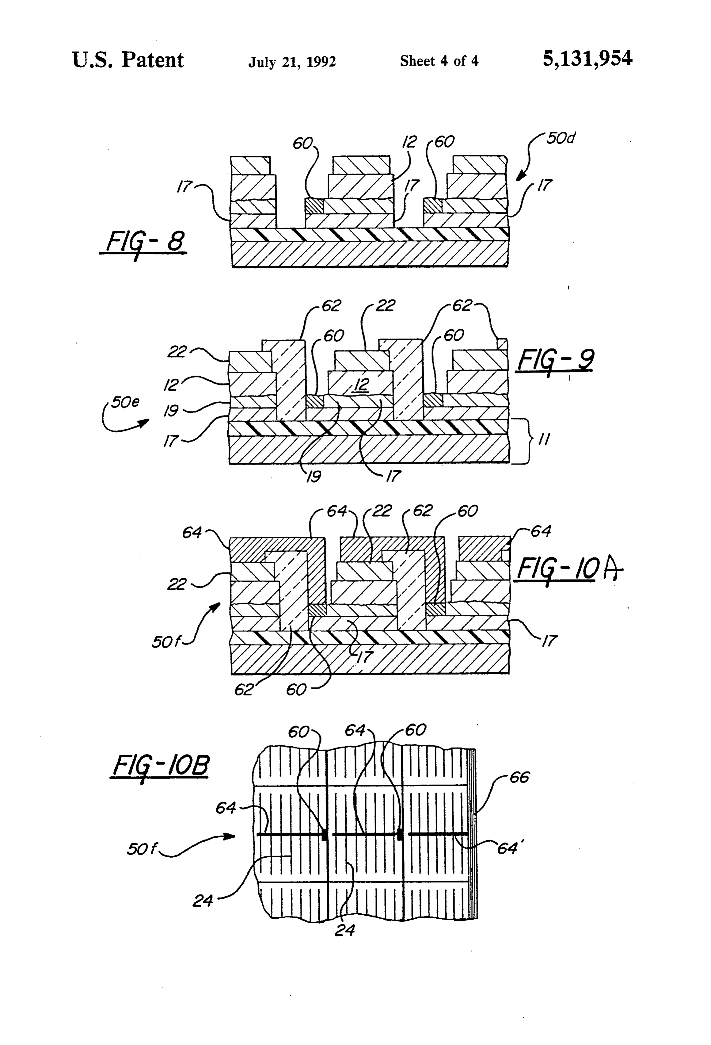
device of FIG. 4A illustrating two contact pad areas: Disposed atop the semiconductor layers is a body of FIG. 5 is a cross-sectional view showing the device of transparent conductive oxide (TCO) 22. This layer FIG. 4B at a second stage of processing: 35 functions as the upper electrode of the device and coop FIG. 6A is a top plan view of the monolithic photo erates with the bottom contact layer 17 to establish a voltaic device at a third stage of processing: current path through the device 10. An electrode grid FIG. 6B is a cross-sectional view of a portion of the 24 may be added to the device where the cell is of a device of FIG. 6A illustrating two of the contact pad sufficiently large area, or if the conductivity of the TCO areas thereof; layer 22 is insufficient. The grid 24 shortens the carrier FIG. 7 is a cross-sectional view showing the device at path through the TCO and thus increases the conduc a fourth stage of processing: tion efficiency of the cell 10. FIG. 8 is a cross-sectional view showing the device at As noted hereinabove, large area photovoltaic de a fifth stage of processing; vices having a structure generally similar to that of the FIG. 9 is a cross-sectional view showing the device at 45 device 10 of FIG. 1, may be fabricated in a continuous a sixth stage of processing; roll-to-roll process. Turning now to FIG. 2, a diagram FIG. 10A is a cross-sectional view showing a portion matic representation of a multiple glow discharge of the completed monolithic device of the present in chamber deposition apparatus for the continuous pro vention; and duction of photovoltaic cells is generally illustrated by FIG. 10B is a top planned view of a portion of a 50 the reference numeral 26. The apparatus 26 includes a completed monolithic area of the present invention. plurality of isolated, dedicated deposition chambers, DETAILED DESCRIPTION OF THE each chamber of which is interconnected by a gas gate
INVENTION
through which sweep gases and a web of substrate material 11 are adapted to pass.
Referring now to the drawings and particularly to 55 The apparatus 26 is adapted to mass produce, in the FIG. 1, a photovoltaic cell formed of a plurality of preferred embodiment, a large area, semiconductor cell successive P-I-N layers, each of which includes, in the having a P-I-N, or N-I-P configuration. The apparatus preferred embodiment, an amorphous semiconductor 26 includes at least one triad of deposition chambers 28, alloy material, is shown generally by the numeral 10. 30, 32. Each triad of deposition chambers comprises a The monolithic array of the present invention may be 60 first chamber 28 in which a p-type conductivity semi comprised of a plurality of subcells, each of which is conductor layer is deposited onto the substrate 11 as it generally similar to that illustrated in FIG. 10, it being passes therethrough, a second deposition chamber 30 in understood that other configurations of cell as well as which an intrinsic amorphous semiconductor layer is other alloy materials may be similarly employed. deposited atop the p type alloy layer as a substrate 11 More particularly, FIG. 1 shows a tandem P-I-N type 65 passes therethrough and a third deposition chamber 32 photovoltaic device such as a solar cell made up of in which an in type conductivity semiconductor layer is stacked, individual P-I-N type cells 12a, 12b and 12c. deposited atop the intrinsic layer as the substrate 11 Below the lower cell 12a is a substrate 11, which in the passes therethrough. It should be apparent that al
Page 8
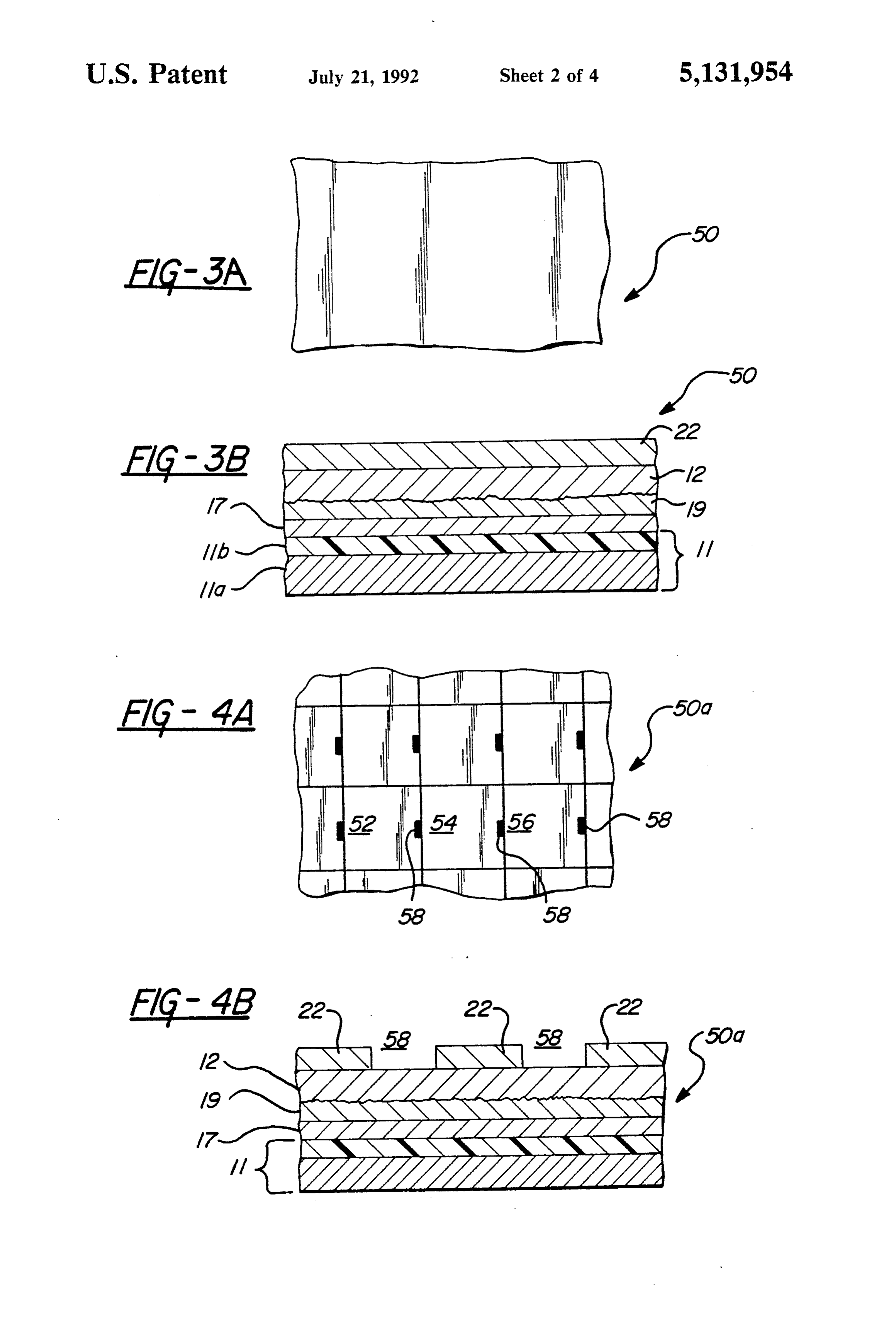
S 6 though one triad of the deposition chambers has been strate, bottom electrode material, semiconductor mate illustrated, additional triads, or additional chambers, rial and top electrode material, which composite consti may be added to the apparatus to provide the capability tutes one very large photovoltaic device. As mentioned of producing cells having an number of stacked P-I-N herein above, it is generally desirable to subdivide this type semiconductor layers. It should be kept in mind large area device into a plurality of small devices inter that the deposition chamber of FIG. 2 is illustrative of connected in a series and/or parallel array so as to in- . one apparatus for the manufacture of the large area crease the device voltage and provide defect and dam body of photovoltaic material and various other deposi age tolerance.
tion techniques such as evaporation, electroplating, Referring now to FIG. 3A there is shown a top plan plasma spray and the like may be similarly employed. 10 view of a large area body of composite photovoltaic Each deposition chamber 28, 30 and 32 of the triad is material 50. FIG. 3B illustrates this body of material 50 adapted to deposit a single semiconductor layer by in cross-section and it will be seen from the figure that glow discharge deposition of a feed gas. To that end, the body is comprised of an electrically insulating sub each of the deposition chambers 28, 30 and 32 includes strate 11, which in this instance is comprised of a body a cathode 34, a shield 35 disposed about each of the 5 of stainless steel of approximately 8 mils thickness 11a cathodes 34, a process gas supply conduit 36 for intro having an insulating body, such as a layer of a polymer ducing process gas mixtures into the area adjacent the such as polyimide 11b thereupon. Composite substrates cathode, a power source 38 such as an alternating cur of this type are disclosed in U.S. Pat. No. 4,514,583, the rent generator, an evacuation conduit 41 for removing disclosure of which is incorporated herein by reference. unused or spent process gases and non-deposited plasma 20 It is to be understood that the present invention may be components, a plurality of transversely extending mag implemented utilizing any substrate provided it is elec netic elements 50, a plurality of radiant heating elements trically insulating and is capable of supporting the semi shown schematically as 40, and a gas date 42 opera conductor and electrode layers thereupon. Among such tively connecting the intrinsic deposition chamber to other substrates are free standing films of polymeric each of the chambers. Further, inert sweep conduits 37 25 material, ceramic, glass and the like. are disposed on opposed sides of the intrinsic deposition Immediately atop the substrate layer 11 is a bottom chamber 30 for establishing a unidirectional flow of electrode layer 17 which, in this instance, is formed inert gas through the gas gate 42. Although the gas from a vacuum deposited layer of aluminum. The bot gates 42 are depicted as establishing a unidirectional tom electrode layer 17 has a highly reflecting surface flow of inert gas, the gas gates 42 may also have other 30 and further functions to redirect light which has passed types of internal flow of sweep gas established as long as through the semiconductor layer back through that the flow operates to prevent diffusion of process gas layer so as to further increase device efficiency. between the adjacent deposition chambers. In the illustrated embodiment, a layer 19 of a tex The supply conduits 36 are operatively associated tured, relatively transparent, relatively conductive with the respective cathodes 34 to deliver process gas 35 oxide material is disposed atop the bottom electrode mixtures to the plasma regions which are created in layer 17. This layer 19 has a roughened or textured top each deposition chamber between said cathodes 34 and (i.e., light facing) side and functions to scatter light a substrate 11. The cathode shields 35 are adapted to passing therethrough so as to cause reflected light to operate in conjunction with the web of substrate mate strike the semiconductor body an oblique angle and rial 11 and the evacuation conduit 41 to substantially 40 thereby increases total internal reflection and hence cell confine the plasma within the cathode region of the efficiency. The layer 19 preferably also has a conductiv deposition chambers. ity adjusted to cause it to act as a "buffer' to large The alternating current generators 38 operate in con current flows. This layer thus functions to limit passage junction with the cathodes 34, the radiant heaters 40 of relatively large amounts of current through the cell, and the ground and substrate 11 to form the plasma and 45 as would occur if the cell developed an internal short. disassociate the process gases entering the plasma re Relatively lower densities of current which flow during gion of the deposition chambers into deposition species normal operation of the cell are not significantly in which form a semiconductor layer upon the substrate. peded. The textured layer 19 together with the reflec The substrate 11 may be maintained substantially flat by tive bottom electrode 17, constitute what is termed a the plurality of rows of magnetic elements 50. 50 textured back reflector.
To form the photovoltaic cell 10 of FIG. 1, a p-type Immediately atop the textured layer 19 is a semicon semiconductor layer is deposited onto the substrate 11 ductor body 12, which may constitute the aforemen in the deposition chamber 28, an intrinsic, amorphous tioned amorphous silicon or germanium alloy or it may semiconductor layer is deposited atop the p-type layer comprise any other thin film semiconductor material in the deposition chamber 30, and an n-type semicon 55 such as polycrystalline silicon, amorphous silicon-car ductor layer is deposited atop the intrinsic layer in the bon alloy materials, polycrystalline germanium, copper deposition chamber 32. As a result, the apparatus 26, indium diselenide, cadmium sulfide, cadmium selenide, deposits at least three successive semiconductor layers gallium arsenide, or the like. Disposed atop the semi onto the substrate 11 and the intrinsic layer deposited in conductor body 12 is a top electrode layer 22 comprised deposition chamber 30 differs in composition from the of a transparent conductive oxide material such as in layers deposited in deposition chambers 28 and 32 by dium oxide, tin oxide or combinations thereof as noted the absence of at least one element which will be re with regard to FIG. 1.
ferred to as the dopant or doping species. In order to In the first step of processing, the large area body of form subsequent stacked P-I-N type cells, the substrate photovoltaic material is subdivided into what will be is either rewound and run through the chambers again come a plurality of small area subcells. Referring now or an apparatus including addition triads is employed. to FIG. 4A there is shown the large area device 50a as The photovoltaic material provided by the apparatus subdivided. Subdivision is accomplished by etching of FIG. 2 may be considered to be a composite of sub through the transparent conductive oxide layer 22 so as
Page 9
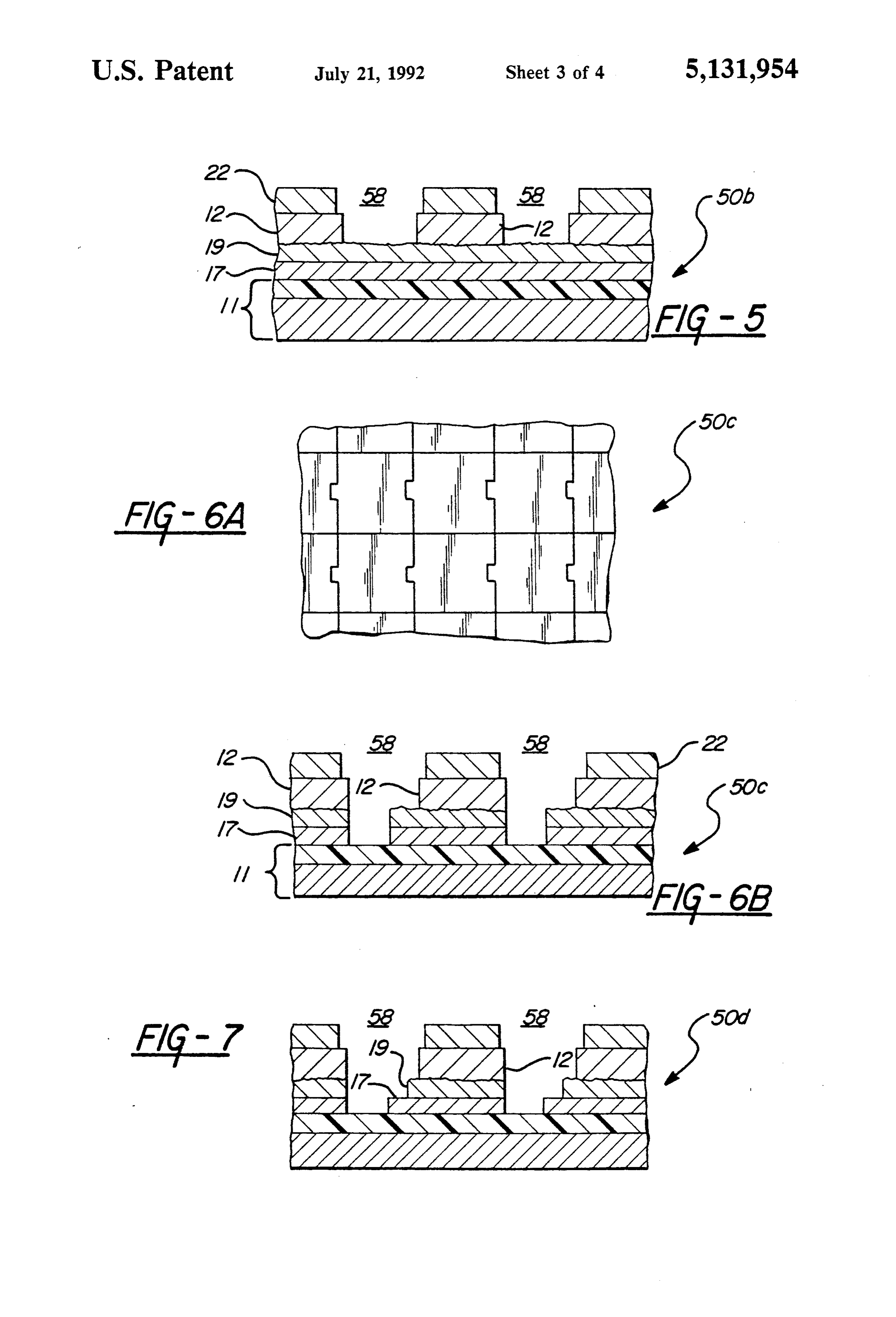
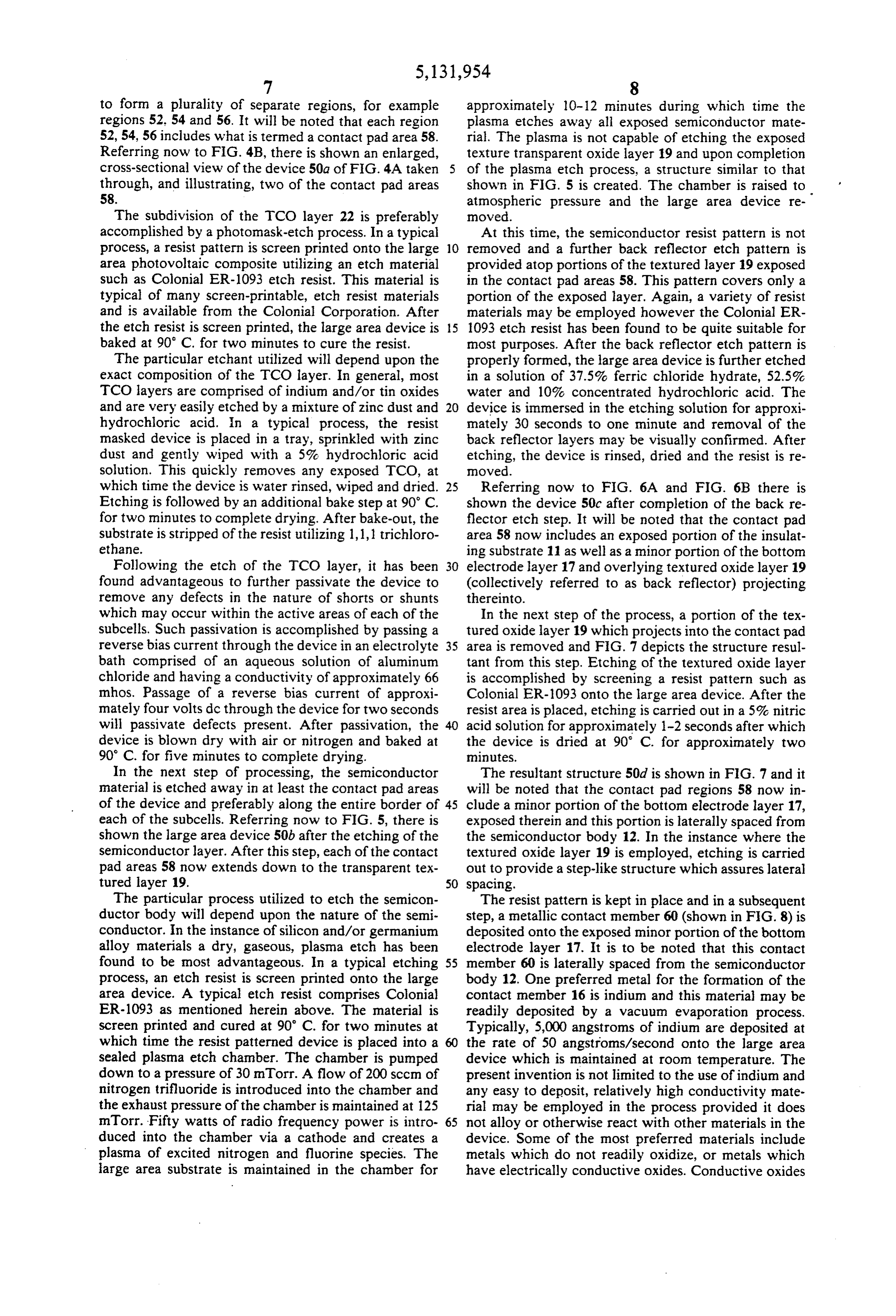
to form a plurality of separate regions, for example approximately 10-12 minutes during which time the regions 52.54 and 56. It will be noted that each region plasma etches away all exposed semiconductor mate 52, 54, 56 includes what is termed a contact pad area 58. rial. The plasma is not capable of etching the exposed Referring now to FIG. 4B, there is shown an enlarged, texture transparent oxide layer 19 and upon completion cross-sectional view of the device 50a of FIG. 4A taken of the plasma etch process, a structure similar to that through, and illustrating, two of the contact pad areas shown in FIG. 5 is created. The chamber is raised to 58. atmospheric pressure and the large area device re The subdivision of the TCO layer 22 is preferably moved.
accomplished by a photomask-etch process. In a typical At this time, the semiconductor resist pattern is not process, a resist pattern is screen printed onto the large 10 removed and a further back reflector etch pattern is area photovoltaic composite utilizing an etch material provided atop portions of the textured layer 19 exposed such as Colonial ER-1093 etch resist. This material is in the contact pad areas 58. This pattern covers only a typical of many screen-printable, etch resist materials portion of the exposed layer. Again, a variety of resist and is available from the Colonial Corporation. After materials may be employed however the Colonial ER the etch resist is screen printed, the large area device is 15 1093 etch resist has been found to be quite suitable for baked at 90 C. for two minutes to cure the resist. most purposes. After the back reflector etch pattern is The particular etchant utilized will depend upon the properly formed, the large area device is further etched exact composition of the TCO layer. In general, most in a solution of 37.5% ferric chloride hydrate, 52.5% TCO layers are comprised of indium and/or tin oxides water and 10% concentrated hydrochloric acid. The and are very easily etched by a mixture of zinc dust and 20 device is immersed in the etching solution for approxi hydrochloric acid. In a typical process, the resist mately 30 seconds to one minute and removal of the masked device is placed in a tray, sprinkled with zinc back reflector layers may be visually confirmed. After dust and gently wiped with a 5% hydrochloric acid etching, the device is rinsed, dried and the resist is re solution. This quickly removes any exposed TCO, at moved.
which time the device is water rinsed, wiped and dried. 25 Referring now to FIG. 6A and FIG. 6B there is Etching is followed by an additional bake step at 90° C. shown the device 50c after completion of the back re for two minutes to complete drying. After bake-out, the flector etch step. It will be noted that the contact pad substrate is stripped of the resist utilizing 1,1,1 trichloro area 58 now includes an exposed portion of the insulat ethane. ing substrate 11 as well as a minor portion of the bottom Following the etch of the TCO layer, it has been 30 electrode layer 17 and overlying textured oxide layer 19 found advantageous to further passivate the device to (collectively referred to as back reflector) projecting remove any defects in the nature of shorts or shunts thereinto.
which may occur within the active areas of each of the In the next step of the process, a portion of the tex subcells. Such passivation is accomplished by passing a tured oxide layer 19 which projects into the contact pad reverse bias current through the device in an electrolyte 35 area is removed and FIG. 7 depicts the structure resul bath comprised of an aqueous solution of aluminum tant from this step. Etching of the textured oxide layer chloride and having a conductivity of approximately 66 is accomplished by screening a resist pattern such as mhos. Passage of a reverse bias current of approxi Colonial ER-1093 onto the large area device. After the mately four volts dc through the device for two seconds resist area is placed, etching is carried out in a 5% nitric will passivate defects present. After passivation, the acid solution for approximately 1-2 seconds after which device is blown dry with air or nitrogen and baked at the device is dried at 90 C. for approximately two 90° C. for five minutes to complete drying. minutes.
In the next step of processing, the semiconductor The resultant structure 50d is shown in FIG. 7 and it material is etched away in at least the contact pad areas will be noted that the contact pad regions 58 now in of the device and preferably along the entire border of 45 clude a minor portion of the bottom electrode layer 17, each of the subcells. Referring now to FIG. 5, there is exposed therein and this portion is laterally spaced from shown the large area device 50b after the etching of the the semiconductor body 12. In the instance where the semiconductor layer. After this step, each of the contact textured oxide layer 19 is employed, etching is carried pad areas 58 now extends down to the transparent tex out to provide a step-like structure which assures lateral tured layer 19. 50 spacing.
The particular process utilized to etch the semicon The resist pattern is kept in place and in a subsequent ductor body will depend upon the nature of the semi step, a metallic contact member 60 (shown in FIG. 8) is conductor. In the instance of silicon and/or germanium deposited onto the exposed minor portion of the bottom alloy materials a dry, gaseous, plasma etch has been electrode layer 17. It is to be noted that this contact found to be most advantageous. In a typical etching 55 member 60 is laterally spaced from the semiconductor process, an etch resist is screen printed onto the large body 12. One preferred metal for the formation of the area device. A typical etch resist comprises Colonial contact member 16 is indium and this material may be ER-1093 as mentioned herein above. The material is readily deposited by a vacuum evaporation process. screen printed and cured at 90° C. for two minutes at Typically, 5,000 angstroms of indium are deposited at which time the resist patterned device is placed into a 60 the rate of 50 angstroms/second onto the large area sealed plasma etch chamber. The chamber is pumped device which is maintained at room temperature. The down to a pressure of 30 mTorr. A flow of 200 sccm of present invention is not limited to the use of indium and nitrogen trifluoride is introduced into the chamber and any easy to deposit, relatively high conductivity mate the exhaust pressure of the chamber is maintained at 125 rial may be employed in the process provided it does mTorr. Fifty watts of radio frequency power is intro 65 not alloy or otherwise react with other materials in the duced into the chamber via a cathode and creates a device. Some of the most preferred materials include plasma of excited nitrogen and fluorine species. The metals which do not readily oxidize, or metals which large area substrate is maintained in the chamber for have electrically conductive oxides. Conductive oxides
Page 10
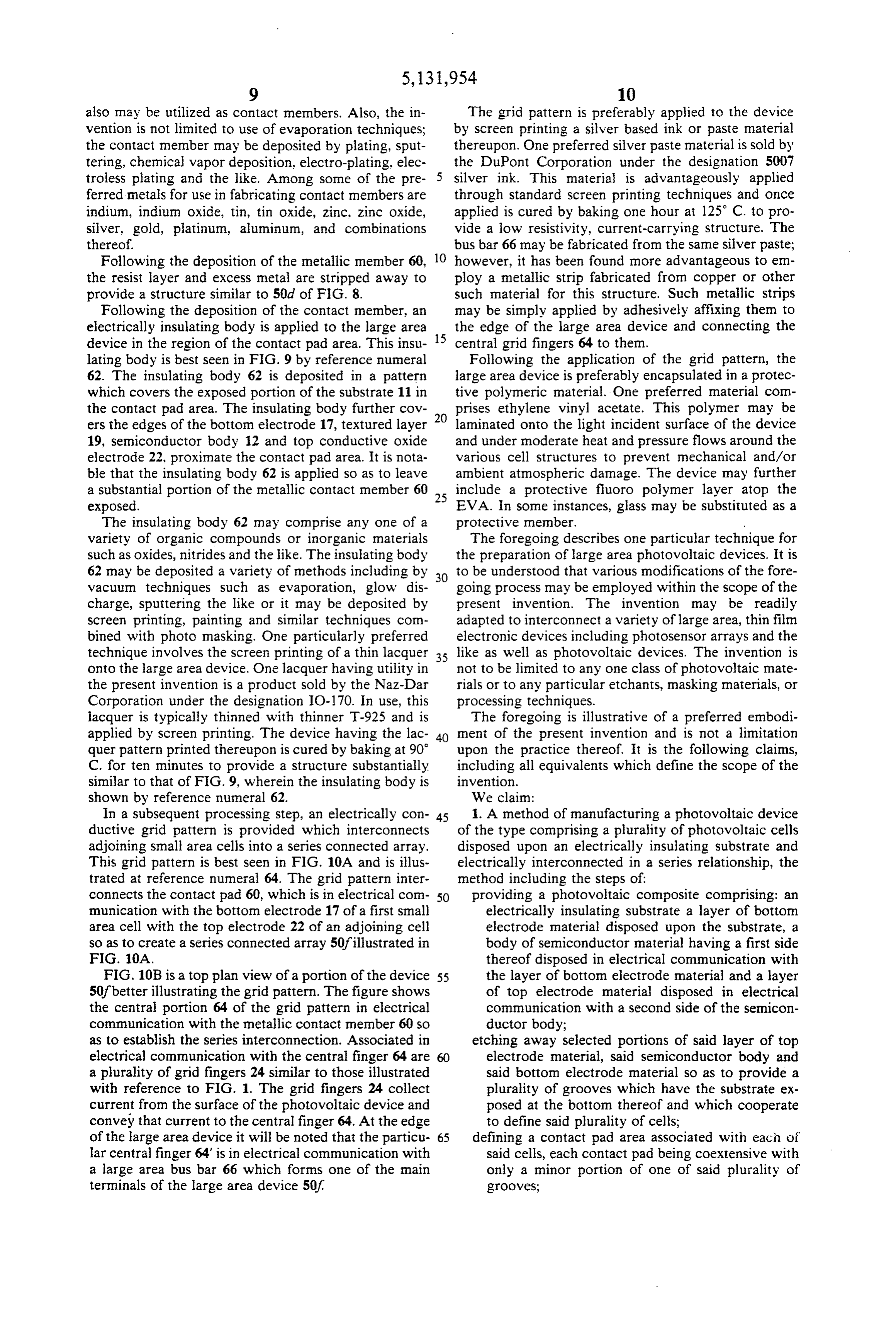
also may be utilized as contact members. Also, the in The grid pattern is preferably applied to the device vention is not limited to use of evaporation techniques; by screen printing a silver based ink or paste material the contact member may be deposited by plating, sput thereupon. One preferred silver paste material is sold by tering, chemical vapor deposition, electro-plating, elec the DuPont Corporation under the designation 5007 troless plating and the like. Among some of the pre silver ink. This materia is advantageously applied ferred metals for use in fabricating contact members are through standard screen printing techniques and once indium, indium oxide, tin, tin oxide, zinc, zinc oxide, applied is cured by baking one hour at 125 C. to pro silver, gold, platinum, aluminum, and combinations vide a low resistivity, current-carrying structure. The thereof. bus bar 66 may be fabricated from the same silver paste; Following the deposition of the metallic member 60, 10 however, it has been found more advantageous to en the resist layer and excess metal are stripped away to ploy a metallic strip fabricated from copper or other provide a structure similar to 50d of FIG. 8. such material for this structure. Such metallic strips Following the deposition of the contact member, an may be simply applied by adhesively affixing them to electrically insulating body is applied to the large area the edge of the large area device and connecting the device in the region of the contact pad area. This insu 5 central grid fingers 64 to them.
lating body is best seen in FIG. 9 by reference numeral Following the application of the grid pattern, the 62. The insulating body 62 is deposited in a pattern large area device is preferably encapsulated in a protec which covers the exposed portion of the substrate 11 in tive polymeric material. One preferred material con the contact pad area. The insulating body further cov 20 prises ethylene vinyl acetate. This polymer may be ers the edges of the bottom electrode 17, textured layer laminated onto the light incident surface of the device 19, semiconductor body 12 and top conductive oxide and under moderate heat and pressure flows around the electrode 22, proximate the contact pad area. It is nota various cell structures to prevent mechanical and/or ble that the insulating body 62 is applied so as to leave ambient atmospheric damage. The device may further a substantial portion of the metallic contact member 60 25 include a protective fluoro polymer layer atop the exposed. EVA. In some instances, glass may be substituted as a The insulating body 62 may comprise any one of a protective member.
variety of organic compounds or inorganic materials The foregoing describes one particular technique for such as oxides, nitrides and the like. The insulating body the preparation of large area photovoltaic devices. It is 62 may be deposited a variety of methods including by 30 to be understood that various modifications of the fore vacuum techniques such as evaporation, glow dis going process may be employed within the scope of the charge, sputtering the like or it may be deposited by present invention. The invention may be readily screen printing, painting and similar techniques corn adapted to interconnect a variety of large area, thin film bined with photo masking. One particularly preferred electronic devices including photosensor arrays and the technique involves the screen printing of a thin lacquer 35 like as well as photovoltaic devices. The invention is onto the large area device. One lacquer having utility in not to be limited to any one class of photovoltaic mate the present invention is a product sold by the Naz-Dar rials or to any particular etchants, masking materials, or Corporation under the designation IO-170. In use, this processing techniques.
lacquer is typically thinned with thinner T-925 and is The foregoing is illustrative of a preferred embodi applied by screen printing. The device having the lac 40 ment of the present invention and is not a limitation quer pattern printed thereupon is cured by baking at 90 upon the practice thereof. It is the following claims, C. for ten minutes to provide a structure substantially including all equivalents which define the scope of the similar to that of FIG. 9, wherein the insulating body is invention.
shown by reference numeral 62. We claim:
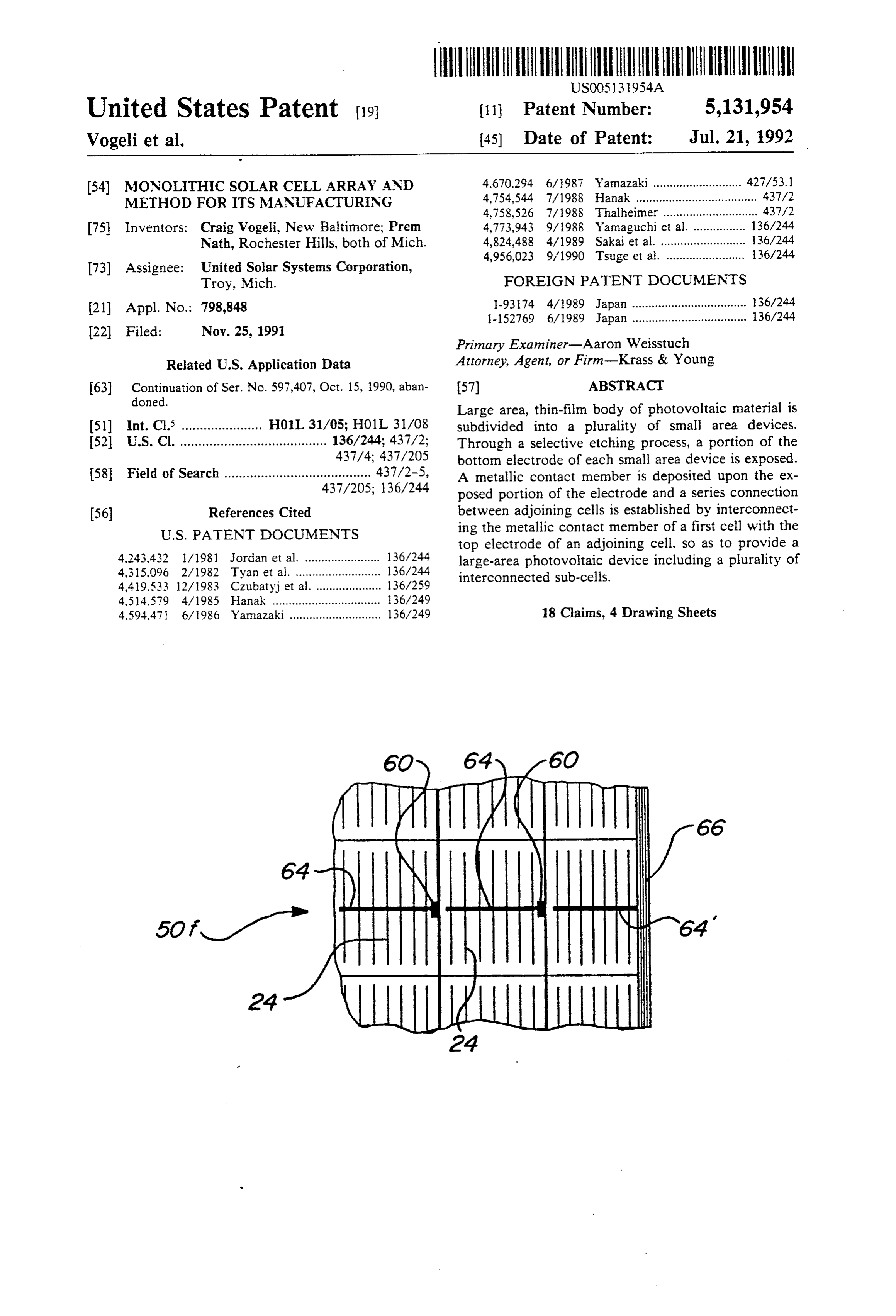
In a subsequent processing step, an electrically con 45 1. A method of manufacturing a photovoltaic device ductive grid pattern is provided which interconnects of the type comprising a plurality of photovoltaic cells adjoining Small area cells into a series connected array. disposed upon an electrically insulating substrate and This grid pattern is best seen in FIG. 10A and is illus electrically interconnected in a series relationship, the trated at reference numera 64. The grid pattern inter method including the steps of:
connects the contact pad 60, which is in electrical con 50 providing a photovoltaic composite comprising: an munication with the botton electrode 17 of a first small electrically insulating substrate a layer of botton area cell with the top electrode 22 of an adjoining cell electrode material disposed upon the substrate, a so as to create a series connected array 50fillustrated in body of semiconductor material having a first side FIG 10A. thereof disposed in electrical communication with FIG. 10B is a top plan view of a portion of the device 55 the layer of botton electrode material and a layer 50fbetter illustrating the grid pattern. The figure shows of top electrode material disposed in electrical the central portion 64 of the grid pattern in electrical communication with a second side of the semicon communication with the metallic contact member 60 so ductor body;
as to establish the series interconnection. Associated in etching away selected portions of said layer of top electrical communication with the central finger 64 are electrode material, said semiconductor body and a plurality of grid fingers 24 similar to those illustrated said bottom electrode material so as to provide a with reference to FIG. 1. The grid fingers 24 collect plurality of grooves which have the substrate ex current from the surface of the photovoltaic device and posed at the bottom thereof and which cooperate convey that current to the central finger 64. At the edge to define said plurality of cells; of the large area device it will be noted that the particu 65 defining a contact pad area associated with eacn of lar central finger 64 is in electrical communication with said cells, each contact pad being coextensive with a large area bus bar 66 which forms one of the main only a minor portion of one of said plurality of terminals of the large area device 50f grooves;
Page 11
etching away the top electrode material and the body 12. A large area photovoltaic device of the type con of semiconductor material in each of said contact prising a plurality of series-connected cells disposed on pad areas so as to define an exposed portion of the an electrically insulating substrate, said device compris bottom electrode material corresponding to said ing:
contact pad area; 5 an electrically insulating substrate; vacuum depositing a contact member upon each of a composite photovoltaic body comprising a bottom said exposed portions of bottom electrode material, electrode layer disposed on said substrate, a layer said contact member being laterally spaced from of semiconductor material disposed atop the bot the semiconductor body; tom electrode layer and a layer of top electrode depositing a body of an electrically insulating mate 10 material disposed atop the layer of semiconductor rial upon the portions of the substrate exposed in material, said photovoltaic body further including the portion of each groove which is coextensive a first and a second group of grooves defined with a respective one of said contact pad areas and therein, each groove extending through the top controlling the depositing of said electrically insu electrode layer, semiconductor layer and bottom lating material so that the contact member is sub 15 electrode layer so as to expose a portion of the stantially free of said insulating material; and substrate at the bottom thereof, the grooves of the disposing an electrically conductive interconnect first group each intersecting the grooves of the member in electrical contact with the contact second group at an angle so as to define a plurality member of a first cell and the top electrode mem of electrically isolated photovoltaic cells; ber of an adjacent cell, whereby series electrical 20 each of said cells including a contact pad area which communication is established therebetween. is defined by an exposed portion of the layer of 2. A method as in claim 1, wherein the steps of etch bottom electrode material which is free of the layer ing away portions of the layer of top electrode material, of top electrode material and the layer of semicon etching away portions of the semiconductor material, ductor material, the contact area of each cell is and etching away portions of the layer of bottom elec disposed to adjoin and be coextensive with only a trode material further comprise etching away said mate 25 minor portion of the length of a groove of the first rials in a pattern which defines the plurality of photo group;
voltaic cells. a contact member disposed upon the exposed portion 3. A method as in claim 1, wherein the step of provid of the layer of bottom electrode material disposed ing a photovoltaic composite further comprising pro 30 in the contact pad area of each cell; viding a layer of transparent, electrically conductive a body of electrically insulating material disposed in, material interposed between said layer of bottom elec and filling, that portion of each groove of the first trode material and the first side of said semiconductor group which adjoins the contact pad area of a cell; body. and 4. A method as in claim 1, wherein said body of semi an electrically conductive member associated with conductor material includes at least one triad of super 35 each cell and disposed so as to electrically commu posed layers of P, I, and N-type semiconductor materi nicate with the bottom electrode of that cell and als. the top electrode of an adjoining cell whereby a 5. A method as in claim 1, wherein said body of semi series electrical connection is established therebe tWeen.
conductor material includes at least one layer of an amorphous silicon alloy material. 13. A photovoltaic device as in claim 12, wherein the 6. A method as in claim 3, including the further step photovoltaic body thereof includes at least one triad of of etching away a portion of the transparent electrically superposed layers of P-type, I-type, and N-type semi conductive material in each of said contact pad areas conductor14. A material.
photovoltaic device as in claim 12, wherein said concomitant with the step of etching away said portion body of photovoltaic material of the layer of bottom electrode material, said etched of a semiconductor material includes
selected at least one layer from the group away portions being generally coextensive. consisting of amorphous silicon alloy materials, amor 7. A method as in claim 6, including a further step phous which is implemented after the etching away of the carbon germanium alloy alloy materials, amorphous silicon materials, polycrystalline silicon, poly portions of transparent conductive material and bottom crystalline germanium, cadmium electrode material, which step comprises: etching away nide, copper indium diselenide, sulfide,
gallium cadmium sele arsenide, and a additional portion of the transparent conductive mate combinations thereof.
rial which overlies the minor portion of the layer of 15. A photovoltaic device as in claim 12, wherein said bottom electrode material in each of said contact pad contact member comprises a material selected from the areas, whereby a portion of the bottom electrode layer, group consisting of indium, indium oxide, tin, tin oxide, free of overlying materials, is exposed. 55 silver, gold, aluminum, zinc, platinum, zinc oxide, and 8. A method as in claim 1, wherein the a contact combinations thereof.
member comprises a member selected from the group 16. A photovoltaic device as in claim 12, wherein the consisting of indium, indium oxide, tin, tin oxide, zinc, electrically conductive member comprises a screen zinc oxide, silver, gold, and combinations thereof. printed pattern of electrically conductive paste. 9. A method as in claim 1, wherein the electrically 17. A photovoltaic device as in claim 12, wherein insulating material comprises a layer of lacquer. each of said cells includes a current collecting grid 10. A method as in claim 1, wherein the step of dis pattern associated in electrical communication with the posing an electrically conductive interconnect member electrically conductive member.
comprises printing a pattern of electrically conductive 18. A photovoltaic device as in claim 12, wherein the paste onto the photovoltaic device. 65 bottom electrode layer comprises a reflective, metallic 11. A method as in claim 10, wherein the step of material having a layer of textured, transparent, electri printing a pattern of electrically conductive paste com cally conductive material disposed thereatop. prises printing a pattern including grid fingers. k k k k
Provenance
- Collection
- Cited prior art
- Original PDF
- patentimages.storage.googleapis.com →
- Filed
- 1991-11-25
- Pages
- 11
- Method
- pdftotext (the PDF's own text layer) + pdftoppm 300dpi page scans
- Source
- Google Patents bibliographic record
- Granted
- 1992-07-21
- Inventors
- Craig Vogeli; Prem Nath; United Solar Systems Corp
- Transcribed from
- patentimages.storage.googleapis.com →