patent · US5087949
Light-emitting diode with diagonal faces
11 February 1992
Page 1 — bibliographic record
HHHHHHH
United States Patent (19) 11) Patent Number: 5,087,949 Haitz (45) Date of Patent: Feb. 11, 1992
54) LIGHT-EMITTING DODE WITH
FOREIGN PATENT DOCUMENTS
DIAGONAL FACES
75 Inventor: Roland H. Haitz, Portola Valley, 52-058492 5/1977 Japan ..................................... 357/55 Calif. 0.058878 4/1984 Japan ....
(73) Assignee: Hewlett-Packard Company, Palo 0244890 10/1988 Japan ..................................... 357/17 Alto, Calif. OTHER PUBLICATIONS (21) Appl. No.: 666,467 IEEE Transactions on Electron Devices, ED-24, No. 22) Fied: Mar. 5, 1991 7, Jul. 1977; "A GaP Monolithic Numeric Display with Internal Reflection Facets'; pp. 979–982.
Related U.S. Application Data
Patent Abstracts of Japan, vol. 7, NO. 123 (E-178)
(63) Continuation of Ser. No. 582,803, Sep. 13, 1990, aban K.K.) 09 Mar. 1983.
doned, which is a continuation of Ser. No. 372,275, Primary Examiner-Andrew J. James
Assistant Examiner-Stephen D. Meier 51 Int. Cl. ....................... H01L 33/00; H01L 9/31; (57) ABSTRACT
(52) U.S.C. ........................................ 357/17; 357/60; A transparent light-emitting diode has front and back 357/68; 357/55; 357/65 parallel faces and a plurality of side faces perpendicular (58) Field of Search ....................... 357/17, 55, 68, 60, to the back face. Diagonal faces interconnect each side 357/30, 65 face with the front face to form a truncated polygonal pyramid surmounting a polygonal base of the light (56) References Cited emitting diode. Because some of the light impinges on
for total internal reflection, from 1.5 to 2 times as much 3,739,217 6/1973 Bergh et al. ........................ 313/108 light is extracted from the LED as a conventional rect 3,900,863 8/1975 Kim ................ ... 357/17 angular LED without the diagonal faces. The diagonal 3,997,907 12/1976 Nakamura ...... ... 357/17. faces on the LEDs are readily made by sawing V 4,080,245 3/1978 Yamanaka ...... ... 357/17 4,217,689 8/1980 Fujii et al.............................. 29/583 shaped grooves in the front face of a wafer on which the 4,234,792 l/1980 Delou et al. ....... 250/36 R. LEDs are fabricated.
4,856,014 8/1989 Figueroa et al. ..................... 372/46 4,864,371 9/1989 Steranka ................................ 357/17 17 Claims, 3 Drawing Sheets
as NCAA Nasriyyy
OCON 2A 4
Page 2
Drawing sheet — no readable text.
Page 3
Drawing sheet — no readable text.
Page 4
Drawing sheet — no readable text.
Page 5
where the side faces are smooth crystallographic planes
LIGHT-EMTTING DODE WITH DAGONAL intersecting the front and back surfaces. FACES An LED chip has six orthogonal surfaces and there fore six possible escape cones. In such a rectangular
This application is a continuation of Ser. No. 582,803, body reflected rays never change their angle of inci filed Sept. i3, 1990, which is a continuation of Ser. No. dence. In other words, rays emitted in a direction out 372,275, filed June 27, 1989, which are both now aban side of the six escape cones will always remain outside doned. of the escape cones no matter how many reflections they experience. Such rays keep bouncing around
FIELD OF THE INVENTION O within the LED until they eventually are absorbed. This invention relates to a transparent light-emitting Four of the escape cones directed at the side surfaces diode with light output up to twice the light output of a are unobstructed. The cone directed towards the back conventional light-emitting diode. contact surface is partly absorbed and partly reflected towards the front. The cone directed towards the front
BACKGROUND OF THE INVENTION 15 is partly transmitted through the front and partly oc In recent years the light-emitting diode (LED) has culted and absorbed by the front electrical contact. As become a commonplace device for a broad range of athrough result, in a typical transparent LED light is extracted only about five cones or approximately 25% of applications. In the visible range it may provide com munication between an electronic device and the user. the light generated by the LED is actually emitted. In the infrared range it may have broad applications for 20 When the LED is operating in air instead of in trans communications. It may be used in an optical isolator parent plastic, emission is even poorer since the critical for decoupling an input signal from an output. In many angle for total internal reflection is only about 16° to 18. For this reason it is customary to operate LEDs.
applications it is an important desideratum that the embedded in transparent plastic for maximum light LED emits a large amount of light for a given current. 25 extraction efficiency.
Transparent LEDs emit light at a p-n junction within the body of semiconductor forming the LED. Light is forByexample making the chip an imperfect rectangular body, by sawing the chip instead of cleaving it, emitted in all directions from the junction and because somewhat roughened of the transparency of the device, light may be emitted is scattered from suchside faces may be obtained. Light roughened surfaces from non from its four sides and its front surface. The back sur 30 escape directions into the escape cones. Some light face is opaque, but some light may be reflected from it within the escape cones may be internally reflected and emitted through the sides or front. A portion of the from a roughened surface. Further, the randomizing of front surface may be occulted by the need for an electri the light directions requires many reflections and be cal contact. Thus, light may be emitted from four sides cause of the non-negligible level of absorption, the long and a portion of the front. 35 light path within the LED results in only a modest Extracting light from an LED is not easy because of increase in extraction efficiency. the high index of refraction of the semiconductor mate Taken to its ultimate or optimal configuration for rial which may be in the range of from about 2.9 to 4.0, light extraction, a LED would have a surface of a hemi depending on wavelength and material. According to sphere so that light from a small p-n junction in its Snell's law center is normal to the surface regardless of the ray sinées ns/n direction. Such hemispherical LEDs have been built only rays that impinge on the chip surface at an angle because and are highly efficient, but extremely high in price equal to or less than 6 will be refracted through the such priorof hemispherical the complex processing required. Some of
LEDs were made by tempo surface. All rays impinging at angles greater than 6c will 45 rarily connecting two LEDs together base-to-base, then experience total internal reflection. In other words, tumbling them in a rotating polishing only light emitted from a point source within the chip cal. Alternatively, some of the priormillhemispherical until spheri within a cone of total cone angle 26c having its axis LEDs were made by attaching the LED chip to a dop perpendicular to the face of the semiconductor chip will and polishing much as one would polish a lens. The cost escape from the LED. 50 of LEDs made by such techniques is prohibitive for Assuming that the index of refraction, inc, for the most applications.
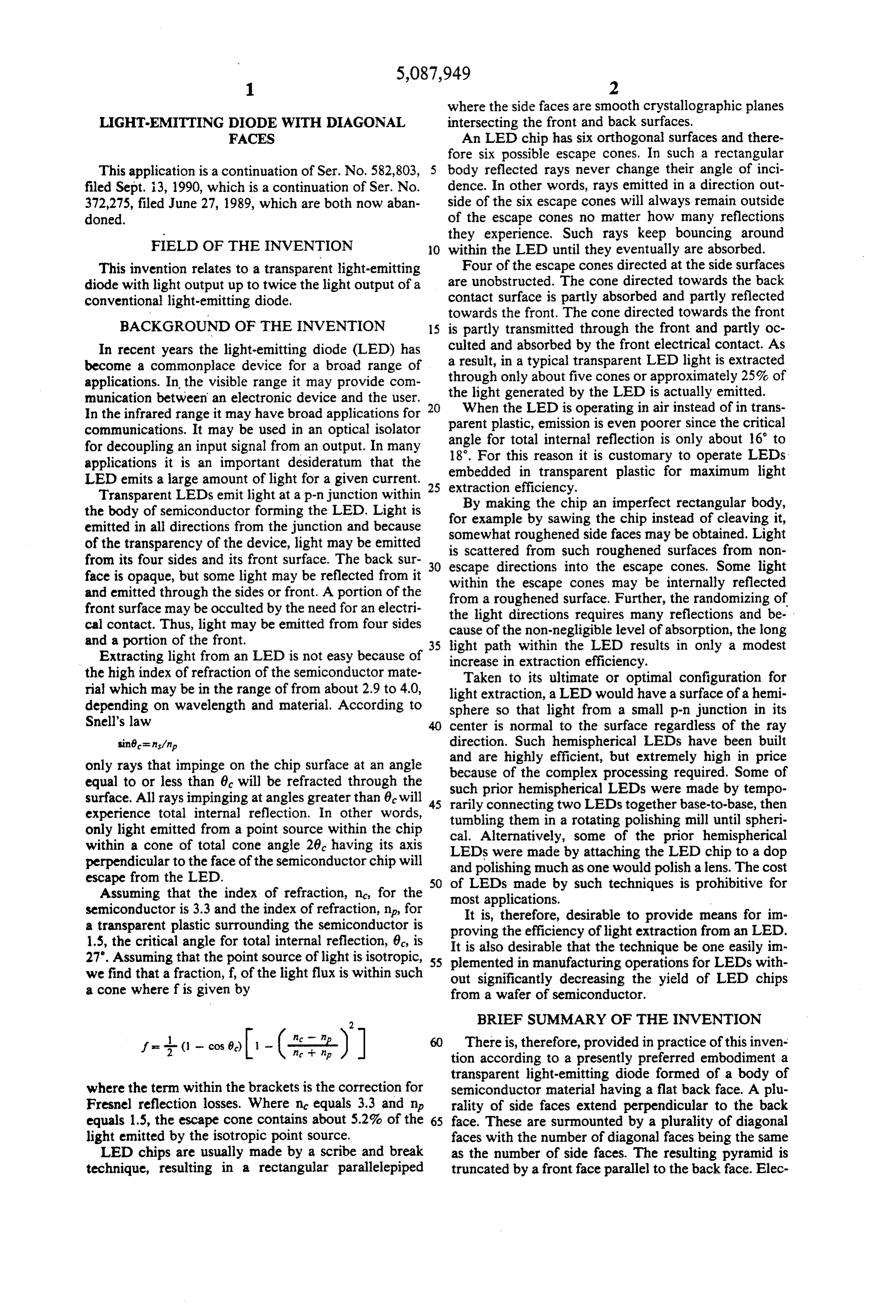
semiconductor is 3.3 and the index of refraction, n, for It is, therefore, desirable to provide means for im a transparent plastic surrounding the semiconductor is proving the efficiency of light extraction from an LED. 1.5, the critical angle for total internal reflection, 6, is It is also desirable that the technique be one easily im 27. Assuming that the point source of light is isotropic, 55 plemented in manufacturing operations for LEDs with we find that a fraction, f, of the light flux is within such out significantly decreasing the yield of LED chips a cone where f is given by from a wafer of semiconductor.
2 BRIEF SUMMARY OF THE INVENTION
1-4-a-co -(iii) There is, therefore, provided in practice of this inven tion according to a presently preferred embodiment a transparent light-emitting diode formed of a body of where the term within the brackets is the correction for semiconductor material having a flat back face. A plu Fresnel reflection losses. Where no equals 3.3 and np rality of side faces extend perpendicular to the back equals 1.5, the escape cone contains about 5.2% of the 65 face. These are surmounted by a plurality of diagonal light emitted by the isotropic point source. faces with the number of diagonal faces being the same LED chips are usually made by a scribe and break as the number of side faces. The resulting pyramid is technique, resulting in a rectangular parallelepiped truncated by a front face parallel to the back face. Elec
Page 6
trical contacted are made with the back and front faces nal face from the side face to the front face subtends an and a p-n junction within the semiconductor body emits angle from the center of the p-n junction in the order of light. twice the critical angle for total internal reflection. Such an LED may have essentially twelve escape Light within a 26 cone from the assumed point source cones, and internal reflections of light which does not in the center of the junction will pass through the diago escape in the first pass has a reasonable probability of nal face.
being reflected into an escape cone. This provides an Since light emitted toward the back face reflector is improvement in extraction efficiency of up to twice the reflected forwardly towards the diagonal face, there is a light from a conventional LED. second escape cone through that diagonal face. In other O words, there are three escape cones of light transmitted
BRIEF DESCRIPTION OF THE DRAWINGS
through the two surfaces 11 and 13 on each of the four
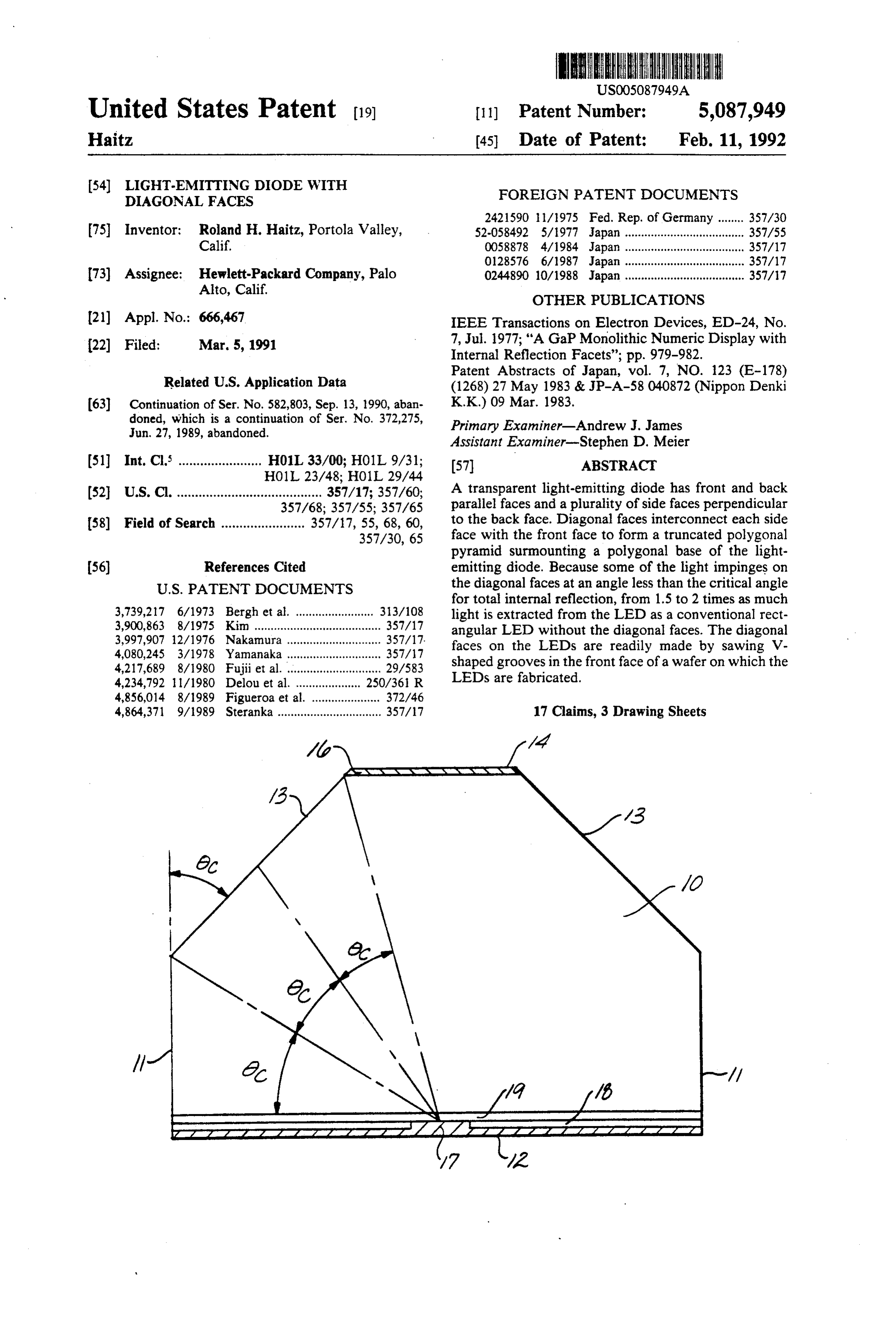
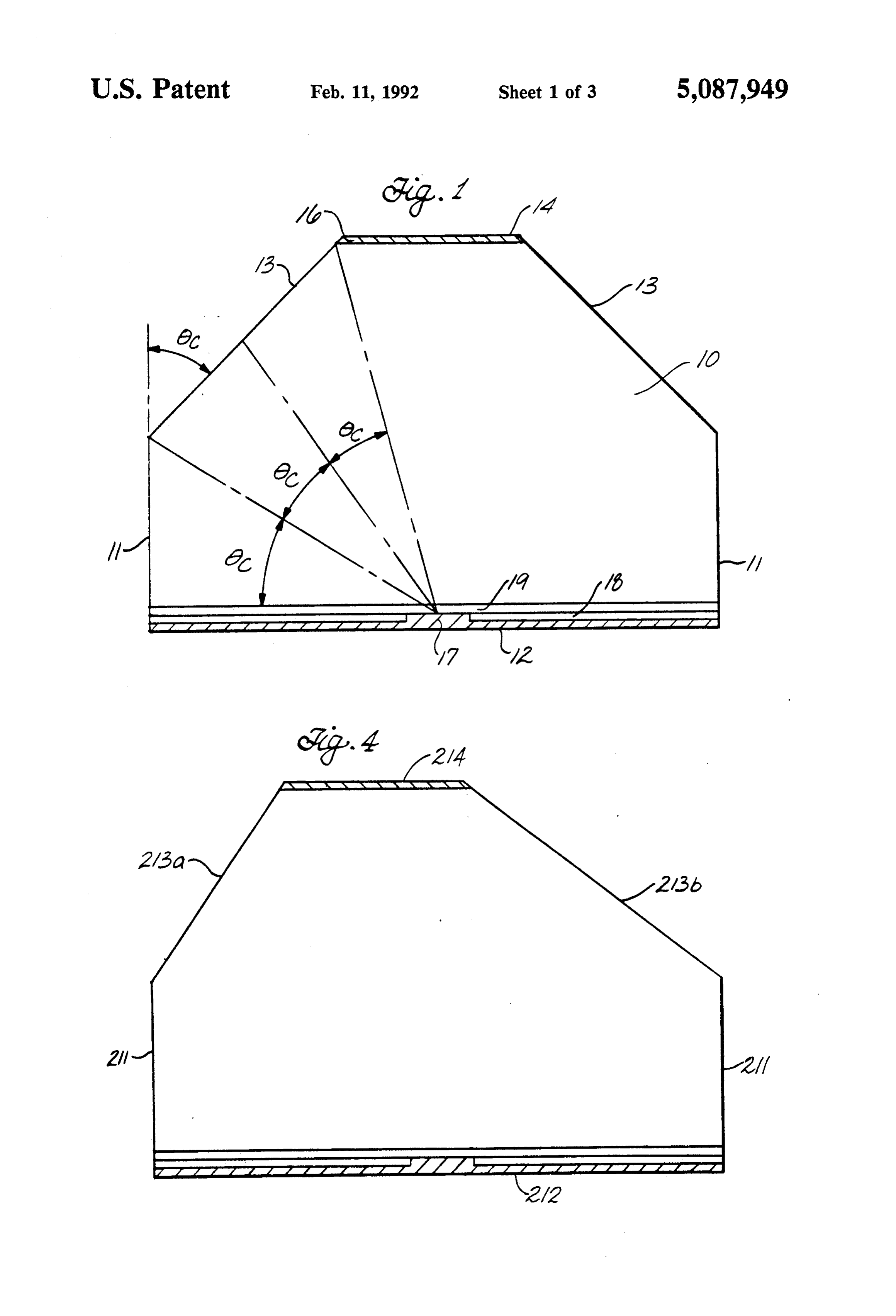
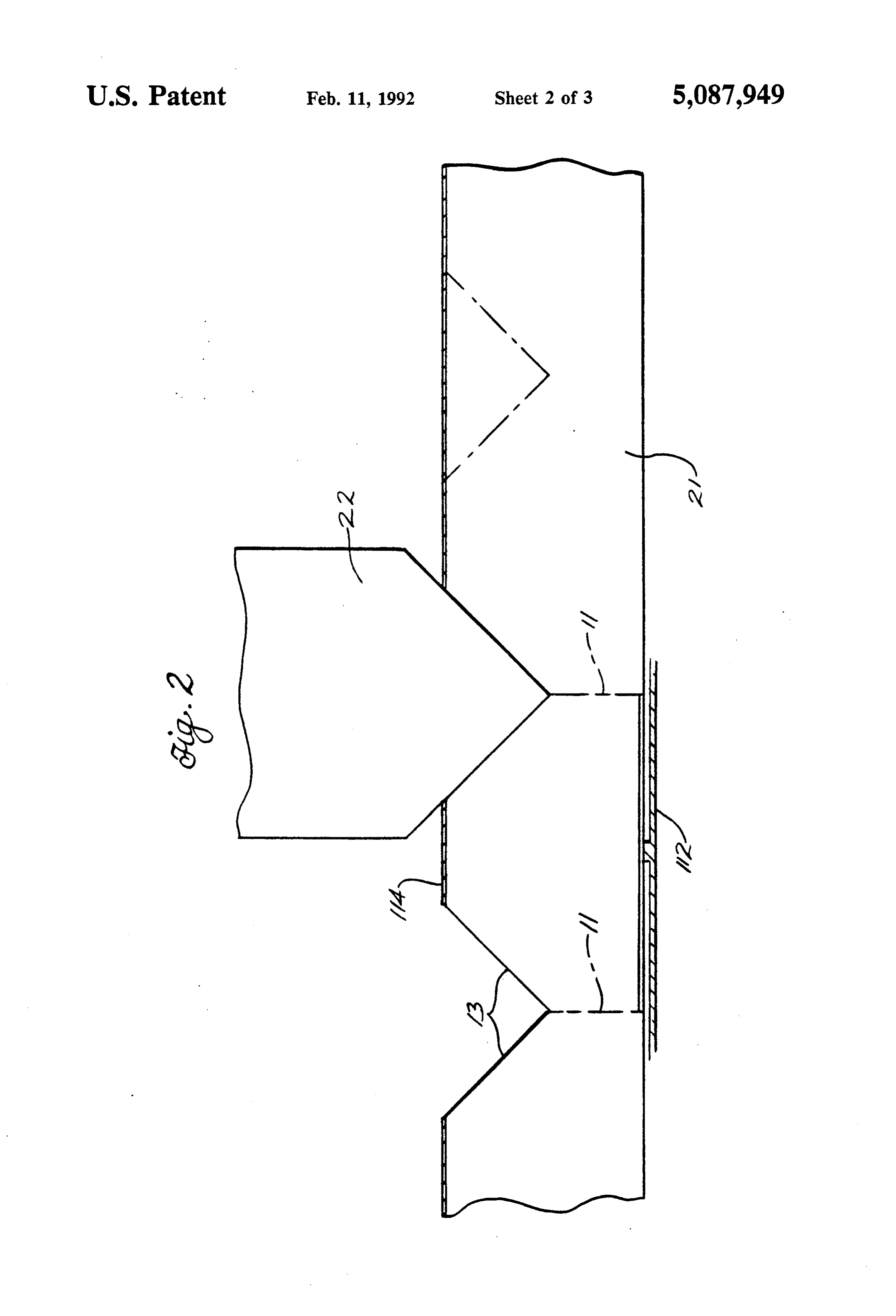
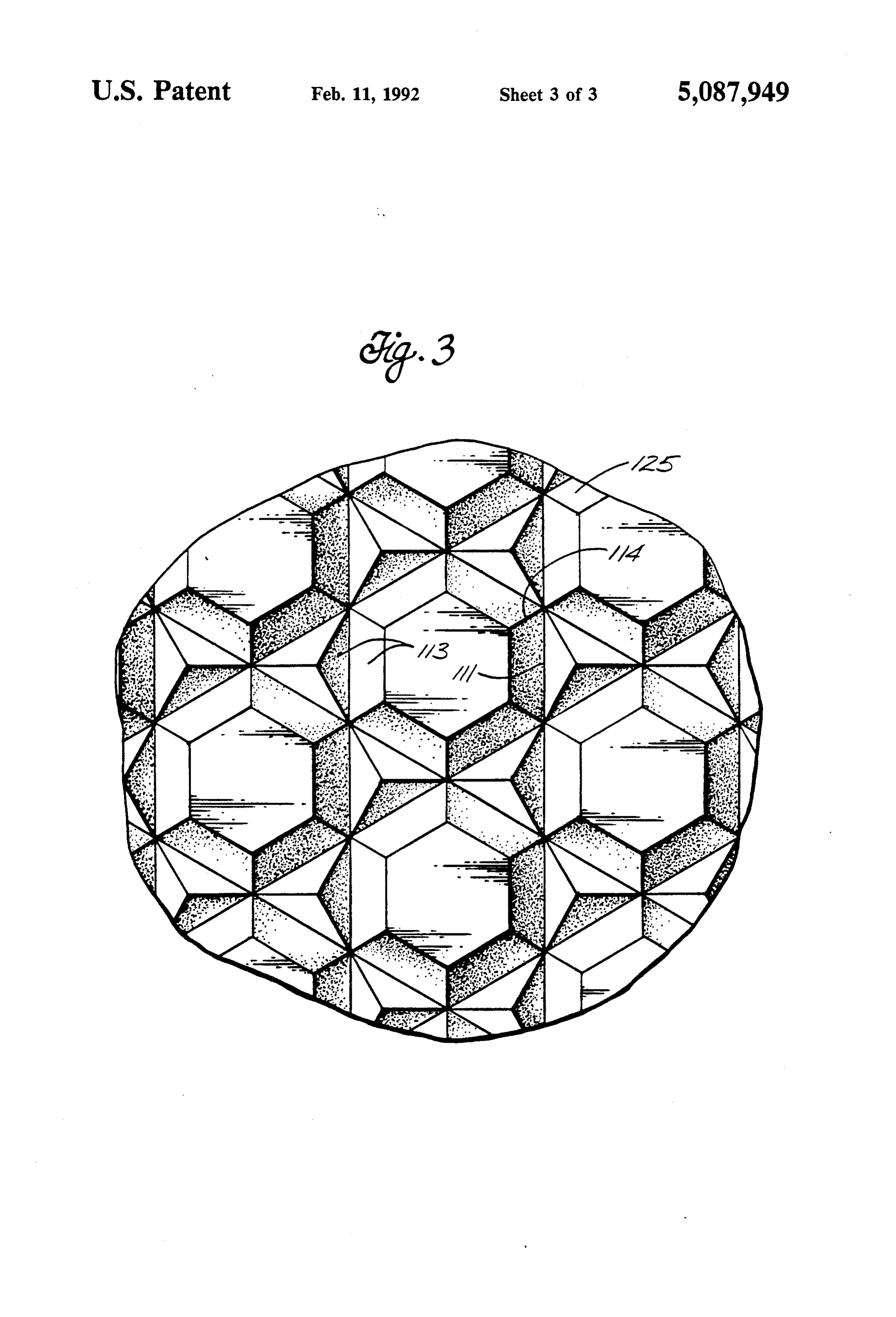
These and other features and advantages of the pres sides of the rectangular body. Thus there are essentially ent invention will be appreciated as the same becomes 12 escape cones which are not significantly affected by better understood by reference to the following detailed metal or contact obstructions.
description of a presently preferred embodiment 15 Light transmitted towards the front contact directly, wherein: or indirectly by reflection from the back face, is at least FIG. 1 is an exemplary transverse cross section of a partly occulted by the opaque electrical contact; hence, light-emitting diode constructed according to principles there is something less than two full cone equivalents of this invention; emitted through the front face of the LED. FIG. 2 illustrates in transverse cross section a tech 20 Thus, there are twelve escape cones containing about nique for cutting a semiconductor wafer for forming a 62% of the emitted light and two cones centered on the plurality of light-emitting diodes; front and back faces containing about 10% of the light FIG. 3 is a fragmentary plan view of one face of a that is absorbed. The remaining 28% of the light emit wafer from which light emitting diodes are cut; and ted has a reasonable probability of being reflected into FIG. 4 illustrates in transverse cross section another 25 one of the twelve escape cones after one or two reflec embodiment of light-emitting diode. tions on the surfaces of the LED. This probability is DETALED DESCRIPTION enhanced when the diagonal faces are non-specular due to slight roughening during the process of manufacture
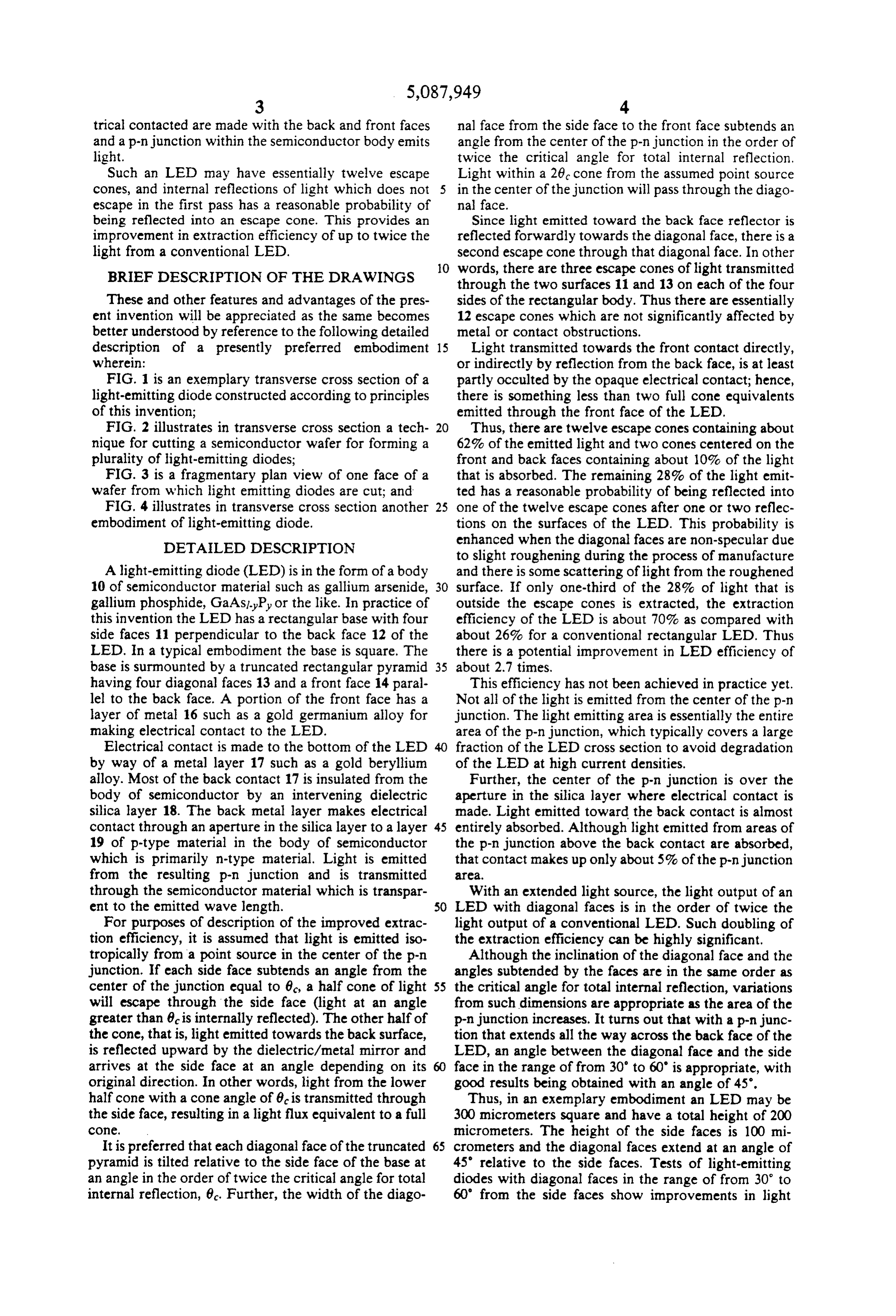
A light-emitting diode (LED) is in the form of a body and there is some scattering of light from the roughened 10 of semiconductor material such as gallium arsenide, 30 surface. If only one-third of the 28% of light that is gallium phosphide, GaAsi-Pyor the like. In practice of outside the escape cones is extracted, the extraction this invention the LED has a rectangular base with four efficiency of the LED is about 70% as compared with side faces 11 perpendicular to the back face 12 of the about 26% for a conventional rectangular LED. Thus LED. In a typical embodiment the base is square. The there is a potential improvement in LED efficiency of base is surmounted by a truncated rectangular pyramid 35 about 2.7 times.
having four diagonal faces 13 and a front face 14 paral This efficiency has not been achieved in practice yet. lel to the back face. A portion of the front face has a Not all of the light is emitted from the center of the p-n layer of metal 16 such as a gold germanium alloy for junction. The light emitting area is essentially the entire making electrical contact to the LED. area of the p-n junction, which typically covers a large Electrical contact is made to the bottom of the LED 40 fraction of the LED cross section to avoid degradation by way of a metal layer 17 such as a gold beryllium of the LED at high current densities.
alloy. Most of the back contact 17 is insulated from the Further, the center of the p-n junction is over the body of semiconductor by an intervening dielectric aperture in the silica layer where electrical contact is silica layer 18. The back metal layer makes electrical made. Light emitted toward the back contact is almost contact through an aperture in the silica layer to a layer 45 entirely absorbed. Although light emitted from areas of 19 of p-type material in the body of semiconductor the p-n junction above the back contact are absorbed, which is primarily n-type material. Light is emitted that contact makes up only about 5% of the p-n junction from the resulting p-n junction and is transmitted area through the semiconductor material which is transpar With an extended light source, the light output of an ent to the emitted wave length. 50 LED with diagonal faces is in the order of twice the For purposes of description of the improved extrac light output of a conventional LED. Such doubling of tion efficiency, it is assumed that light is emitted iso the extraction efficiency can be highly significant. tropically from a point source in the center of the p-n Although the inclination of the diagonal face and the junction. If each side face subtends an angle from the angles subtended by the faces are in the same order as center of the junction equal to 6, a half cone of light 55 the critical angle for total internal reflection, variations will escape through the side face (light at an angle from such dimensions are appropriate as the area of the greater than 8c is internally reflected). The other half of p-n junction increases. It turns out that with a p-n junc the cone, that is, light emitted towards the back surface, tion that extends all the way across the back face of the is reflected upward by the dielectric/metal mirror and LED, an angle between the diagonal face and the side arrives at the side face at an angle depending on its 60 face in the range of from 30 to 60' is appropriate, with original direction. In other words, light from the lower good results being obtained with an angle of 45. half cone with a cone angle of 8c is transmitted through Thus, in an exemplary embodiment an LED may be the side face, resulting in a light flux equivalent to a full 300 micrometers square and have a total height of 200 COne. micrometers. The height of the side faces is 100 mi It is preferred that each diagonal face of the truncated 65 crometers and the diagonal faces extend at an angle of pyramid is tilted relative to the side face of the base at 45' relative to the side faces. Tests of light-emitting an angle in the order of twice the critical angle for total diodes with diagonal faces in the range of from 30° to internal reflection, 6. Further, the width of the diago 60' from the side faces show improvements in light
Page 7
extraction efficiency of from one and one-half to two preferred since the crystal structure of the semiconduc times the light output of a conventional LED of similar tor does not lend itself to crystallographic cleavage at dimensions without the diagonal faces. 60° angles and there is no problem in removing the Fabrication of a LED with beveled edges is a triangular scraps between adjacent LEDs. It will be straightforward adaption of conventional manufactur noted that because of such scraps the yield of hexagonal ing techniques for semiconductors. LEDs are conven LEDs from a wafer is two-thirds of the yield of rectan tionally made in substantial numbers on a wafer of semi gular LEDs. The enhanced light extraction efficiency conductor. Very light scratches may be scribed on a through twelve faces as compared with eight faces in face of the semiconductor to provide a crack initiator. the rectangular embodiment may offset the added cost When broken, the individual LEDs are cleaved from 10 due to decreased yield.
each other along crystallographic planes extending FIG. 4 illustrates in transverse cross section another from the scribe lines. Alternatively, the LEDs are embodiment of LED for high efficiency light extrac sawed from the wafer with a diamond dicing saw. tion. This LED has side faces 211 and a back face 212 To make a beveled LED, an array of parallel V similar to the embodiments hereinabove described. It shaped grooves are sawed into one face of a wafer 21 by 15 differs, however, in that one of the diagonal faces 213a a nearly conventional diamond dicing saw 22. The dic is at a different angle from its adjacent side face 211 than ing saw perimeter is dressed with a V-shaped face to the angle between the opposite side face 213b and its produce diagonal faces 13 on adjacent LEDs to be adjacent side face. A similar asymmetry is provided for separated from the wafer. The depth of the saw cut is the other two diagonal faces not illustrated in the draw controlled to define the desired width of the diagonal 20 ing. As a result of this asymmetry, the front face 214 is faces. shifted diagonally toward one corner of the LED. After sawing arrays of parallel V-shaped grooves in The angular difference between the opposite faces is orthogonal directions, the individual LEDs may be only a few degrees so that there is little degradation of separated from each other by cleaving from the bottom the light extraction efficiency due to an exit cone of of the groove, or a second pass may be made with a 25 light illuminating an area off of a diagonal face. Substan conventional dicing saw aligned with the bottom of the tial degradation may be avoided by choice of dimen groove to cut the balance of the distance through the sions of the side faces and diagonal faces. However, wafer. In still another alternative the face of the dicing extraction efficiency of light internally reflected within saw may be dressed so that the V-shaped groove and the LED is enhanced due to the asymmetrical reflec the parallel-sided cut through the balance of the wafer 30 tions from the diagonal faces.
are made in a single pass of the dicing saw. After saw Such an embodiment with asymmetrical beveling is ing, the sawed surfaces are etched for removing the easily made by the technique described hereinabove by highly absorbing saw damaged material adjacent to the simply dressing the face of the dicing saw with the surface. desired asymmetry, thereby producing an asymmetrical It will be noted that cleaving produces side faces 11 35 V-shaped groove.
of the LEDs which are substantially specular. The diag Although limited embodiments of light-emitting onal faces are slightly roughened due to the diamond diode constructed according to principles of this inven particles in the dicing saw. The side faces are also tion have been described and illustrated herein, many slightly roughened when the LEDs are separated from modifications and variations will be apparent to those each other by sawing. The resultant non-specular re skilled in the art. Thus, for example, in the illustrated flection of light from such faces slightly enhances effi embodiments the p-n junctions is quite near the back ciency of light extraction from the LED. face of the LED. It may be desirable to employ a LED Taken to its ultimate or optimal configuration for where the p-n junction is an appreciable distance above light extraction, a LED would have a surface of a hemi the back face. In such an embodiment it is preferable sphere so that light from the center of the p-n junction 45 that the height of the side faces should subtend an angle is normal to the surface regardless of the ray direction above the center of the junction in the order of the and light from other areas of the p-n junction either critical angle for total internal reflection. Thus, half of exits on the first pass or after a limited number of reflec the light in the exit cone is above the plane of the junc tions. This is not a feasible geometry for semiconductor tion and some of the light may exit the side face below manufacturing techniques. The square LED with bev 50 the plane of the p-n junction.
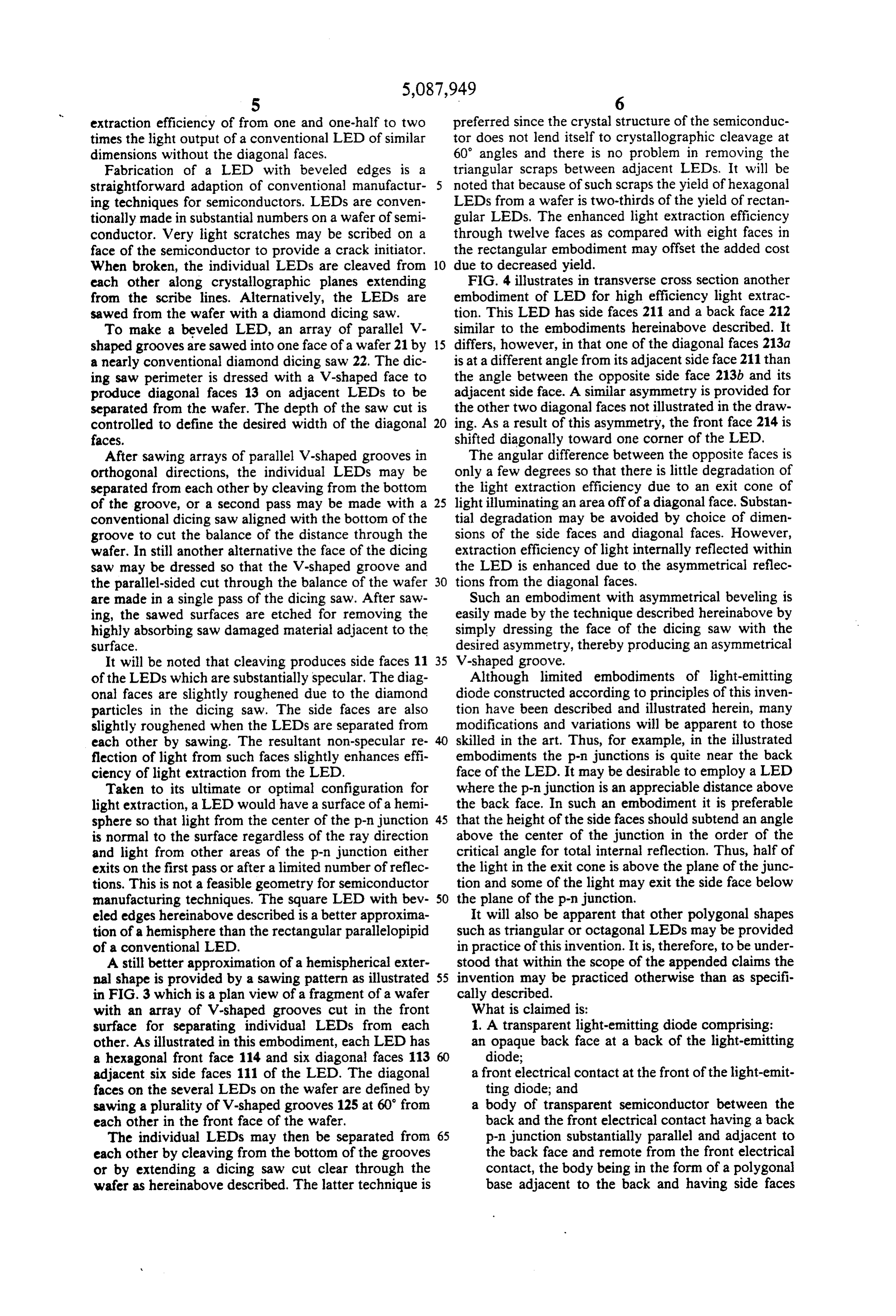
eled edges hereinabove described is a better approxima It will also be apparent that other polygonal shapes tion of a hemisphere than the rectangular parallelopipid such as triangular or octagonal LEDs may be provided of a conventional LED. in practice of this invention. It is, therefore, to be under A still better approximation of a hemispherical exter stood that within the scope of the appended claims the nal shape is provided by a sawing pattern as illustrated 55 invention may be practiced otherwise than as specifi in FIG. 3 which is a plan view of a fragment of a wafer cally described.
with an array of V-shaped grooves cut in the front What is claimed is:
surface for separating individual LEDs from each 1. A transparent light-emitting diode comprising: other. As illustrated in this embodiment, each LED has an opaque back face at a back of the light-emitting a hexagonal front face 114 and six diagonal faces 113 diode;
adjacent six side faces 111 of the LED. The diagonal a front electrical contact at the front of the light-emit faces on the several LEDs on the wafer are defined by ting diode; and sawing a plurality of V-shaped grooves 125 at 60 from a body of transparent semiconductor between the each other in the front face of the wafer, back and the front electrical contact having a back The individual LEDs may then be separated from 65 p-n junction substantially parallel and adjacent to each other by cleaving from the bottom of the grooves the back face and remote from the front electrical or by extending a dicing saw cut clear through the contact, the body being in the form of a polygonal wafer as hereinabove described. The latter technique is base adjacent to the back and having side faces
Page 8
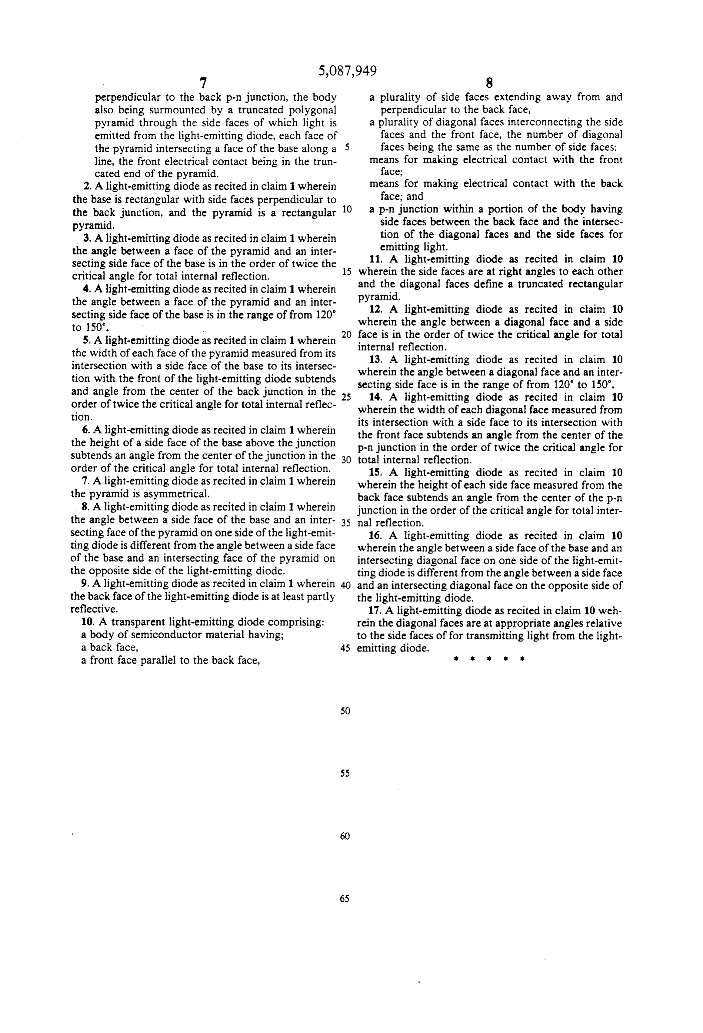
perpendicular to the back p-n junction, the body a plurality of side faces extending away from and also being surmounted by a truncated polygonal perpendicular to the back face, pyramid through the side faces of which light is a plurality of diagonal faces interconnecting the side emitted from the light-emitting diode, each face of faces and the front face, the number of diagonal the pyramid intersecting a face of the base along a 5 faces being the same as the number of side faces: line, the front electrical contact being in the trun means for making electrical contact with the front cated end of the pyramid. face;
2. A light-emitting diode as recited in claim 1 wherein means for making electrical contact with the back the base is rectangular with side faces perpendicular to O face; and the back junction, and the pyramid is a rectangular a p-n junction within a portion of the body having pyramid. side faces between the back face and the intersec 3. A light-emitting diode as recited in claim 1 wherein tion of the diagonal faces and the side faces for the angle between a face of the pyramid and an inter emitting light.
11. A light-emitting diode as recited in claim 10 secting side face of the base is in the order of twice the 15 wherein critical angle for total internal reflection. the side faces are at right angles to each other 4. A light-emitting diode as recited in claim 1 wherein and the diagonal faces define a truncated rectangular the angle between a face of the pyramid and an inter pyramid. 12. A light-emitting diode as recited in claim 10 secting side face of the base is in the range of from 120 wherein the angle between a diagonal face and a side
face is in the order of twice the critical angle for total 5. A light-emitting diode as recited in claim 1 wherein 20 internal reflection.
the width of each face of the pyramid measured from its 13. A light-emitting diode as recited in claim 10 intersection with a side face of the base to its intersec tion with the front of the light-emitting diode subtends secting side angle wherein the face is between a diagonal face and an inter in the range of from 120' to 150'.
and angle from the center of the back junction in the 25 14. A light-emitting order of twice the critical angle for total internal reflec wherein the width of eachdiode as recited in claim 10 diagonal face measured from tlOn.
its intersection with a side face to its intersection with 6. A light-emitting diode as recited in claim 1 wherein the height of a side face of the base above the junction the front face subtends an angle from the center of the p-n junction in the order of twice the critical angle for subtends an angle from the center of the junction in the 30 total internal reflection.
order of the critical angle for total internal reflection. 15. A light-emitting diode as recited in claim 10 7. A light-emitting diode as recited in claim 1 wherein wherein the height of each side face measured from the the pyramid is asymmetrical. back face subtends an angle from the center of the p-n 8. A light-emitting diode as recited in claim 1 wherein junction in the order of the critical angle for total inter the angle between a side face of the base and an inter 35 nal reflection.
secting face of the pyramid on one side of the light-emit 16. A light-emitting diode as recited in claim 10 ting diode is different from the angle between a side face wherein the angle between a side face of the base and an of the base and an intersecting face of the pyramid on intersecting diagonal face on one side of the light-emit the opposite side of the light-emitting diode. ting diode is different from the angle between a side face 9. A light-emitting diode as recited in claim wherein and an intersecting diagonal face on the opposite side of the back face of the light-emitting diode is at least partly the light-emitting diode.
reflective. 17. A light-emitting diode as recited in claim 10 weh 10. A transparent light-emitting diode comprising: rein the diagonal faces are at appropriate angles relative a body of semiconductor material having; to the side faces of for transmitting light from the light a back face, 45 emitting diode.
a front face parallel to the back face,
Provenance
- Collection
- Cited prior art
- Original PDF
- patentimages.storage.googleapis.com →
- Filed
- 1991-03-05
- Pages
- 8
- Method
- pdftotext (the PDF's own text layer) + pdftoppm 300dpi page scans
- Source
- Google Patents bibliographic record
- Granted
- 1992-02-11
- Inventors
- Roland H. Haitz; Hewlett Packard Co
- Transcribed from
- patentimages.storage.googleapis.com →