patent · US3863075
Light emitting diode assembly
28 January 1975
Page 1 — bibliographic record
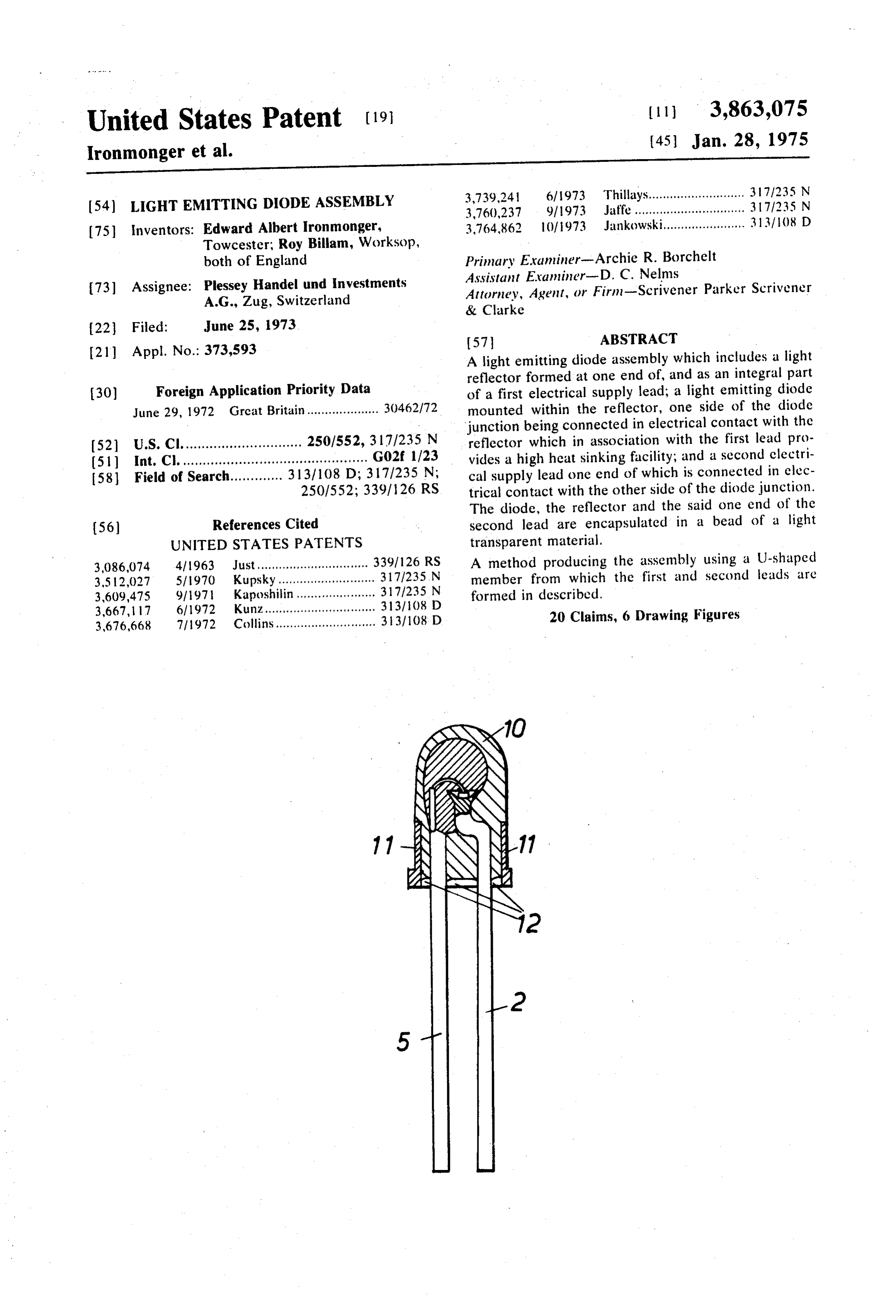
United States Patent (19) [11] 3,863,075 Ironmonger et al. (45) Jan. 28, 1975 3,739,241 6/1973 Thillays........................... 37/235 N (54) LIGHT EMITTING DODE ASSEMBLY 3,760,237 9/1973 Jaffe ............................... 37/235 N 75 inventors: Edward Albert Ironmonger, 3,764862 10/1973 Jankowski....................... 313/108 D Towcester; Roy Billam, Worksop, both of England Primary Examiner-Archie R. Borchelt 73) Assignee: Plessey Handel und Investments Assistant Examiner-D. C. Nelms A.G., Zug, Switzerland Attorney, Agent, or Firn-Scrivener Parker Scrivener & Clarke
21) Appl. No.: 373,593 A light emitting diode assembly which includes a light reflector formed at one end of, and as an integral part (30) Foreign Application Priority Data of a first electrical supply lead; a light emitting diode June 29, 1972 Grcat Britain.................... 30462/72 mounted within the reflector, one side of the diode junction being connected in electrical contact with the (52) U.S. Cl.............................. 250/552, 317/235 N reflector which in association with the first lead pro (5) Int. Cl. .............................................. G02f 1/23 vides a high heat sinking facility; and a second clectri 58) Field of Search............. 313/108 D; 3171235 N; cal supply lead one end of which is connected in elec 250/552; 339/26 RS trical contact with the other side of the diode junction.
The diode, the reflector and the said one end of the 56) References Cited second lead are encapsulated in a bead of a light UNITED STATES PATENTS transparent material.
3,086,074 4, 1963 Just,.............................. 339/126 RS A method producing the assembly using a U-shaped 3,512,027 5/1970 Kupsky........................... 317/235N member from which the first and second leads are 3,609,475 9/1971 Kaposhillin...................... 317/235 N formed in described.
3,667, 17 6/1972 Kunz............................... 313/108 D 20 Claims, 6 Drawing Figures 3,676,668 7/1972 Collins............................ 33/108 D
Page 2
Drawing sheet — no readable text.
Page 3
LIGHT EMITTING DODE ASSEMBLY shaped section 3 and the end 4a of the reduced section 4 are coated with a film of a light reflective contact ma
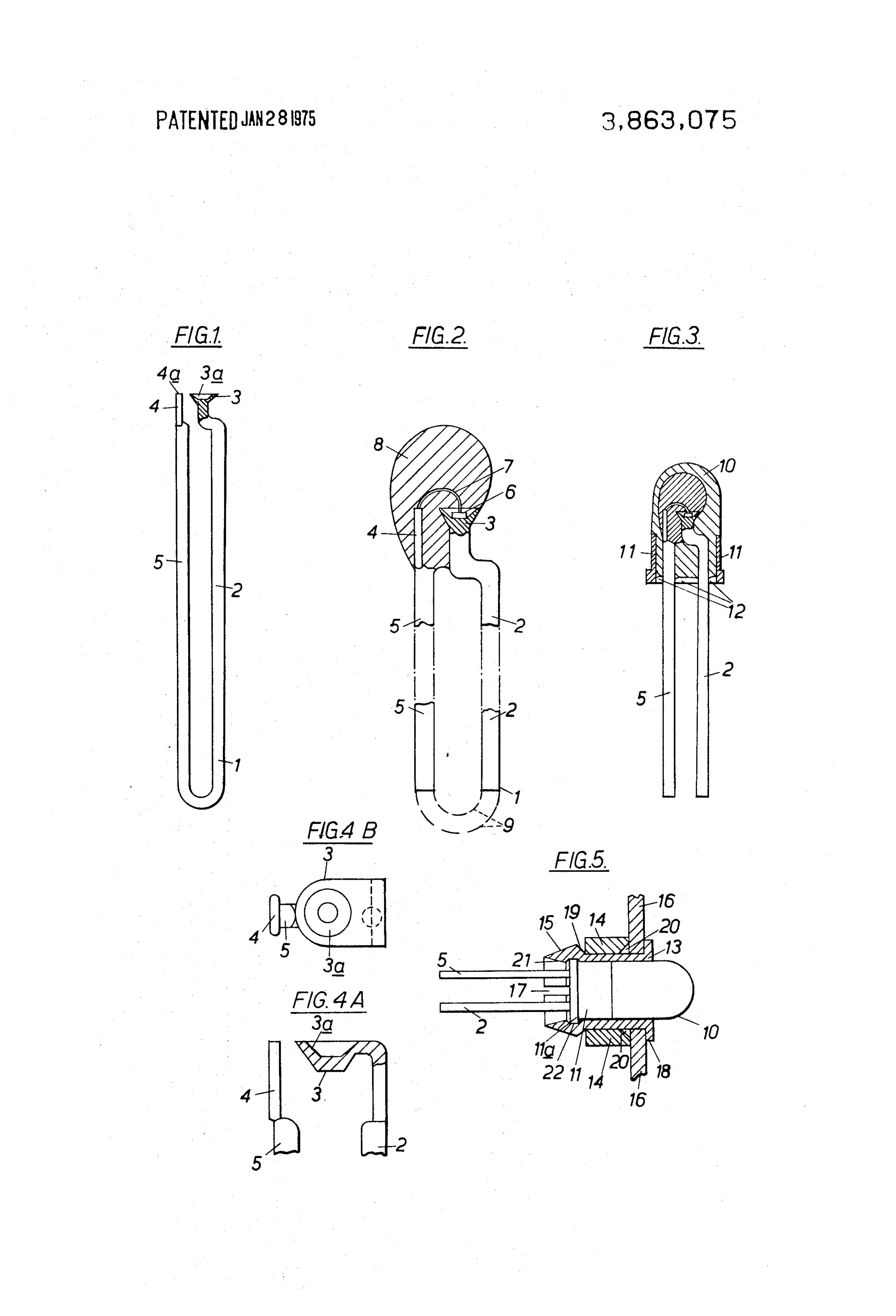
The invention relates to light emitting diode assem terial. Alternatively, the entire outer surface of the U blies and to methods of producing the diode assem shaped member 1 can be coated with a film of the light blies. reflective contact material. The dish-shaped section 3, The invention provides a light emitting diode assem therefore, forms a light reflector.
bly which includes a light reflector formed at one end In practice, the U-shaped member 1 can be of nickel of, and as an integral part of, a first electrical supply plated copper and the light reflective contact material lead; a light emitting diode mounted within the reflec film can be of gold.
tor, one side of the diode junction being connected in 10 In the next stage of the production method a light electrical contact with the reflector; and a second elec emitting diode 6 is provided and, as illustrated in FIG. trical supply lead, one end of which is connected in 2, is mounted within the dish-shaped section 3 such electrical contact with the other side of the diode junc that one side of the diode junction is connected in elec tion, the diode, the reflector and the said one end of the trical contact with the contact material film, the electri second electrical supply lead being encapsulated in a 5 cal connection being effected by means of a solder in bead of a light transparent material. terface, for example a gold/germanium alloy solder. The invention also provides a method of producing The end 4a of the limb 5 is then connected in electri a light emitting diode assembly which includes the steps cal contact with the other side of the diode junction by of providing a U-shaped member of an electrically con means of a fine electrically conductive wire 7, the free ductive material; forming the free end of one limb of 20 ends of which are bonded to the respective contact ar the U into a dish-shaped section; forming a film of a CaS.
light reflective contact material on at least the inner The free ends of the U-shaped member 1 are then im surface of the dish-shaped section; providing and mersed into a light transparent material in liquid form, mounting a light emitting diode within the dish-shaped for example, an epoxy base resin, which hardenes, by section such that one side of the diode junction is con 25 the action of surface tension, over the extremities of nected in electrical contact with the said film; forming the assembly to form, on solidification, a small bead 8 a film of a contact material on at least the free end of which encapsulates the diode assembly. the other limb of the U; connecting the free end of the After the formation of the bead 8, the limbs 2 and 5 said other limb in electrical contact with the other side of the U-shaped member 1 are severed at or near to the of the diode junction; encapsulating the diode, the dish 30 base of the Uthereby removing the base (illustrated by shaped section and the free end of the other limb of the the dotted lines 9 in FIG. 2) and forming two electrical U in a bead of a light transparent material; and severing supply leads for the diode 6.
each limb of the U at or near to the base of the U to The structure of the light emitting diode assembly of provide two electrical supply leads for the diode. FIG. 2 is such that a light reflector i.e. the inner coated The foregoing and other features according to the in 35 surface 3a of the dish-shaped section 3, for enhancing vention will be better understood from the following the appearance of the light emitted by the diode 6 is description with reference to the accompanying draw formed as an integral part of the electrical supply lead ings, in which: 2 and, therefore, a high heat sinking facility is provided FIG. 1 diagrammatically illustrates in a partly sec 40 for the diode 6. Also, the structure of the assembly and tioned front elevation part of a light emitting diode as the use of a U-shaped member in the production sembly according to the invention, method gives rise to a low cost assembly and versatility FIG. 2 diagrammatically illustrates in an enlarged of lead configuration. w partly sectioned front elevation one arrangement for a In another arrangement for a light emitting diode as light emitting diode assembly according to the inven 45 sembly according to the invention which is diagram tion, matically illustrated in FIG.3 of the drawings in a FIG. 3 diagrammatically illustrates in a partly sec partly sectioned front elevation, the diode assembly of tioned front elevation another arrangement for a light FIG. 2 is encapsulated in a transparent material, for ex emitting diode assembly according to the invention, ample, an epoxy base resin, to provide an outer mem FIGS. 4(A) and 4(B) diagrammatically illustrate re 50 ber 10 of a desired form. That part of the member 10 spectively in an enlarged partly sectioned front eleva which extends forwardly of the reflector should, how tion and an enlarged plan view part of a further ar ever, be of a shape, for example dome shaped, which rangement for a light emitting diode assembly accord is such that the light rays emitted by the diode 6 are ra ing to the invention, and diated in a desired manner. The remainder of the mem FIG. 5 diagrammatically illustrates in a partly sec 55 ber 10 which extends backwardly of the reflector can tioned side elevation a panel mounting arrangement for be of regular cross-section, for example, circular. A the light emitting diode assembly of FIG. 3. collar 11 of an opaque material may be provided and In a method according to the invention for producing be secured in position during the formation of the the light emitting diode assembly diagrammatically il member 10. The collar 11 will serve to enhance the ap lustrated in an enlarged partly sectioned front elevation 60 pearance of the assembly and also to minimise the ef in FIG. 2 of the drawings, an electrically conductive U fects of any irregularity or meniscus 12 that may be shaped member such as the member 1 diagrammat present on the lower surface of the member 10. The ically illustrated in FIG. 1 of the drawings, is produced outer shape of the member 10 will be as shown in FIG. such that the free end of the limb 2 of the U is in the 3 irrespective of whether the collar 11 is present or not. form of a dish-shaped section 3 and such that the free 65 In an alternative method according to the invention end 4 of the limb 5 of the U is reduced in section. The the dish-shaped section 3 could be formed in a manner dish-shaped section 3 can be formed by an upsetting or as is diagrammatically illustrated in FIGS. 4(A) and forging operation. The inner surface 3a of the dish 4.(B) of the drawings respectively in an enlarged partly
Page 4
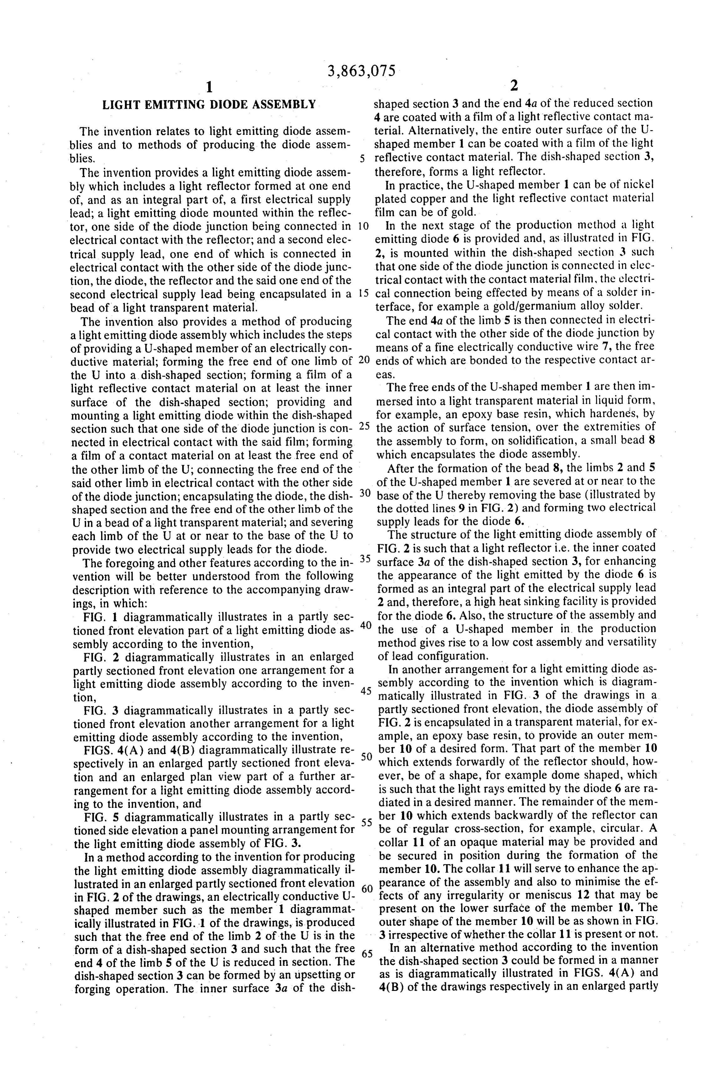
sectioned front elevation and an enlarged plan view. 1. A light emitting diode assembly which includes a With this structure, the section 3 is formed by flatten light reflector formed at one end of, and as an integral ing the free end of the limb 2 of the U-shaped member, part of, a first electrical supply lead; a light emitting forming the dish-shaped section from the flattened por diode mounted within the reflector, one side of the tion and bending the free end of the limb 2 such that diode junction being connected in electrical contact with the reflector; and a second electrical supply lead, the inner surface 3a of the section 3 is uppermost in re one end of which is connected in electrical contact with lation to the base of the U-shaped member. An inter mediate annealing operation may be required in the the other side of the diode junction, the diode, the re formation of the dish-shaped section 3 of FIGS. 4(A) flector and the said one end of the second electrical and 4 (B). O supply lead being encapsulated in a bead of a light A panel mounting arrangement for the light emitting transparent material.
diode assembly of FIG. 3 is diagrammatically illustrated 2. A light emitting diode assembly as claimed in claim in FIG. 5 of the drawings in a partly sectioned side ele 1 wherein the said one end of the second electrical sup vation and includes a flanged bush 13 and a spacing ply lead is connected in electrical contact with the said washer 14. A chamfered end 15 of the bush 13 is 15 other side of the diode junction by means of a electri passed through an aperture of a panel 16, two diametri cally conductive wire.
3. A light emitting diode assembly as claimed in claim cally opposite and longitudinally extending slots (only 1 wherein one slot 17 being illustrated) in the wall of the bush al the light reflective surface of the reflector is lowing the wall of the bush to be inwardly collapsed 20 formed by a film of a light reflective electrical contact and thereby the largest diameter section of the bush to material.
4. A light emitting diode assembly as claimed in claim be passed through the panel aperture. The flange 18 of 1 wherein the bush 13 abuts against the front of the panel 16 and a member the of a light transparent bead is encapsulated in light transparent material, that part of is retained in its abutting relationship with the panel 16 the member which extends upwardly of the reflector by means of the spacing washer 14. The two slots 17 fa 25 being of a shape which is such that the light rays emit cilitate the fitting of the washer 14 to the bush 13 after ted by the diode are radiated in a desired manner, the the bush has been passed through the panel aperture. remainder of the member extending downwardly of the A chamfered annular shoulder 19 on the bush 13 re tains the washer 14 in an abutting relationship with the reflector being of regular cross-section. - back of the panel 16. The bore of the washer 14 is in 30 4 wherein that part of the member which is ofinregular 5. A light emitting diode assembly as claimed claim wardly bevelled at 20, the angle of the bevel 20 being cross-section is provided with a collar of an opaque ma substantially the same as the angle of the chamber 19. terial.
Thus, when the washer 14 is fitted the other way round 6. A light emitting diode assembly as claimed in claim to the bush 13, the chamfer 19 and the bevel 20 co 4 which includes panel mounting means for the encap operate with each other and allow the bush 13 to be re 35 sulated diode.
tained in a panel of greater thickness than the panel 16. 7. A light emitting diode assembly as claimed in claim In order to accommodate an even thicker panel, the 6 wherein the panel mounting means include a bush washer 14 can be dispensed with if the panel thickness having a flange at one end for limiting the insertion of is comparable with the length of that part of the bush the bush into an aperture in a panel, an annular shoul 13 which is situated between the flange 18 and the 40 der with chamfered side edges at the other end, at least chamfer 19. With this arrangement the bush 13 will be two longitudinally extending slots in the bush wall at retained in the panel by means of the chamfer 19 co the said other end for allowing the wall to be inwardly operating with the back of the panel. collapsed and a bore which is adapted to receive, and The bore of the bush 13 at the opposite end to the to retain, the said member in a position whereat the flanged end 18 is chamfered at 21 and is provided with 45 shaped end of the member projects beyond the flanged an annular groove 22 which accommodates a flange end of the bush.
la of the collar 11. Thus, after the bush 13 has been 8. A light emitting diode assembly as claimed in claim secured within the panel 16 the light emitting diode as 7 wherein the length of that portion of the bush be sembly of FIG. 3 is inserted into the bore of the bush 50 tween the flange and the chamfered annular shoulder 13 from the back of the panel 16, the chamfer 21 allow is substantially equal to the thickness of the said panel. ing the flange 11a of the diode assembly to be inserted 9. A light emitting diode assembly as claimed in claim into the bore of the bush and to be snapped into posi 7 wherein the panel mounting means also include a tion in the annular groove 22. The two slots 17 allow spacing washer which has a bore that is adapted to re the bore of the bush to be expanded immediately prior 55 ceive that portion of the bush between the flange and to the flange 11a of the collar 11 being snapped into the chamfered annular shoulder, and which is adapted position in the annual groove 22, the bore of the bush to retain the flange of the bush in an abutting relation returning to its normal shape when the diode assembly ship with the said panel.
is in position. 10. A light emitting diode assembly as claimed in It should be noted that whilst the panel mounting ar 60 claim 9 wherein the spacing washer is of a length less rangement utilises a bush 13 with only two longitudi than the length of the said bush portion by an amount nally extending slots 17, the bush 13 can have three or substantially equal to the thickness of the said panel. four slots to effect the specified functions. 11. A light emitting diode assembly as claimed in It is to be understood that the foregoing description claim 9 wherein the bore of the spacing washer is in of specific examples of this invention is made by way 65 wardly bevelled at one end at substantially the same of example only and is not to be considered as a limita angle as that one of the chamfered side edges of the an tion in its scope. nular shoulder that is contiguous with the said bush What is claimed is: portion, the length of the spacing washer from the
Page 5
S 6 other end thereof to the inner edge of the said bevel mation of the dish-shaped section includes the steps of being less than the length of the said bush portion by flattening the free end of the said one limb; forming the an amount substantially equal to the thickness of the dish-shaped section from the flattened portion; and said panel. bending the free end of the said one limb such that the 12. A method of producing a light emitting diode as inner surface of the dish-shaped portion is uppermost sembly which includes the steps of providing a U in relation to the base of the U-shaped member. shaped member of an electrically conductive material; 16. A method as claimed in claim 12 wherein the said forming the free end of one limb of the U into a dish one side of the diode junction is connected in electrical shaped section; forming a film of a light reflective contact with the said film by means of a solder inter contact material on at least the inner surface of the 10 face.
dish-shaped section; providing and mounting a light 17. A method as claimed in claim 16 wherein the sol emitting diode within the dish-shaped section such that der interface is a gold/germanium alloy solder inter one side of the diode junction is connected in electrical face.
contact with the said film; forming a film of a contact 18. A method as claimed in claim 12 which includes material on at least the free end of the other limb of the 15 the step of encapsulating the light transparent bead in U; connecting the free end of the said other limb in a member of a light transparent material which has a electrical contact with the other side of the diode junc shape forwardly of the reflector that is such that inter tion; encapsulating the diode, the dish-shaped section nal light reflections are minimised, the remainder of the and the free end of the other limb of the U in a bead of a light transparent material; and severing each limb member extending backwardly of the reflector being of of the U adjacent to the base of the U to provide two regular cross-section.
19. A method as claimed in claim 18 which includes electrical supply leads for the diode. the steps of providing a collar of an opaque material; 13. A method as claimed in claim 12 wherein the free end of the said other limb is connected in electrical and securing the collar around that part of the member contact with the other side of the diode junction by 25 which of the is of regular cross-section during encapsulation light transparent bead.
means of a electrically conductive wire. 20. A method as claimed in claim 12 wherein the U 14. A method as claimed in claim 12 wherein the dish-shaped section is formed in the end of the said one shaped member is of nickel plated copper, and wherein limb by an upsetting operation. the light reflective contact
material
is gold.
15. A method as claimed in claim 12 wherein the for 30
Provenance
- Collection
- Cited prior art
- Original PDF
- patentimages.storage.googleapis.com →
- Filed
- 1973-06-25
- Pages
- 5
- Method
- pdftotext (the PDF's own text layer) + pdftoppm 300dpi page scans
- Source
- Google Patents bibliographic record
- Granted
- 1975-01-28
- Inventors
- Edward Albert Ironmonger; Roy Billam; Plessey Handel und Investments AG
- Transcribed from
- patentimages.storage.googleapis.com →