patent · US5046159
Image transmitting element and process for producing same
3 September 1991
Page 1 — bibliographic record
United States Patent (19) 11 Patent Number: 5,046,159 Hamanaka 45 Date of Patent: Sep. 3, 1991 (54) IMAGE TRANSMITTING ELEMENT AND 4,759,603 7/1988 Jones ................................ 350/96.28 PROCESS FOR PRODUCING SAME 4,767, 172 8/1988 Nichols et al. ................... 3SO/96.18 4,874,957 10/1989 Sasaki et al. ..................... 250/208.1 (75) Inventor: Kenjiro Hamanaka, Osaka, Japan 4,942,481 7/1990 Yoshinouchi et al. ......... 358/.484 X 73) Assignee: Nippon Sheet Glass Co., Ltd., Osaka, Primary Examiner-Richard A. Wintercorn Japan Attorney, Agent, or Firn-Sughrue, Mion, Zinn, 21 Appl. No.: 611,601 Macpeak & Seas (22 Filed: Nov. 13, 1990 57 ABSTRACT (30) Foreign Application Priority Data An image transmitting element and a process for pro ducing the same are disclosed, which image transmit
Nov. 24, 1989 (JP) Japan .................................. 1-305893 ting element comprises: a transparent substrate; photo (51) Int. Cl.'....................... G03B 27/00; H01J 40/14; transmissible holes one-dimensionally or two-dimen H04N 3/14; H04N 5/335 sionally formed as an array in the transparent substrate, 52 U.S. C. ................................. 355/001; 250/208.1; each of the holes having one end opened at one surface 358/213.13; 358/484; 385/33; 385/133 of the substrate and the other end made blind and pro 58) Field of Search .................. 350/127, 96.18, 96.28, vided with a substantially spherical top end within a 350/96.34, 96.10; 355/1, 46, 50; 250/227.11, thickness of the substrate; a photo-absorptive surface 208.1; 358/213.13, 484,494 formed on at least a part of an inner surface of each of
the photo-transmissible holes except the surface of the spherical top end thereof; and a transparent material
4,275,962 6/1981 Midorikawa et al. .................. 355/1 transparent material having a refractive index higher 4,472,046 9/1984 Kohyama ................................ 355/1 than that of the substrate.
4,733,096 3/1988 Horiguchi...................... 358/23.13 2 Claims, 3 Drawing Sheets
Page 2
Drawing sheet — no readable text.
Page 3
Drawing sheet — no readable text.
Page 4
Drawing sheet — no readable text.
Page 5
sionally formed as an array in the transparent substrate,
IMAGE TRANSMITTING ELEMENT AND each of the holes having one end opened at one surface PROCESS FOR PRODUCING SAME of the substrate and the other end made blind and pro vided with a substantially spherical top end within a
FIELD OF THE INVENTION thickness of the substrate; a photo-absorptive surface The present invention relates to an image transmit formed on at least a part of an inner surface of each of ting element for optically transmitting and focusing the photo-transmissible holes except the surface of the one-dimensional or two-dimensional image information, spherical top end thereof, and a transparent material and particularly relates to an image transmitting ele O with which the photo-transmissible holes are filled, the ment which is useful for transmitting and focusing an transparent material having a refractive index higher image of an original document onto a contact type than that of the substrate.
image sensor in a copying machine, a facsimile, an The present invention also relates to a process for image scanner, or the like, or transmitting and focusing producing the above image transmitting element, com a light signal from a luminous body array onto a photo 15 prising steps of providing on one surface of each of a sensitive drum in an LED printer or the like. pair of transparent substrates an anti-corrosive mask BACKGROUND OF THE INVENTION film; forming an array of slit openings in parallel to each other, the respective end portions of the slit openings
A lens array (hereinafter abbreviated to "SLA") con being positioned in the inside of the side edge of the stituted by a number of parabolic refractive index dis substrate; contacting an etching material to the surface tributing rod lenses which are arrayed to make their of the substrate on which the mask film is provided so as optical axes parallel has been used broadly to focus to etch the surface of the substrate isotropically from one-dimensional image information on the surface of an the slit openings to thereby form an array of grooves original document onto a contact type image sensor.
Recently, it has been performed to use a so-called 25 each having substantially spherical opposite end sur "perfect contact type image sensor" which is consti part ofproviding faces; a photo-absorptive surface on at least a tuted by a contact type image sensor having light lead spherical opposite endof surfaces an inner wall each of the grooves except the thereof; removing the ing windows, so that an illuminating light source placed mask film; filling the grooves with a transparent mate at the back side of this image sensor illuminates an origi nal document though the light leading window, and an rial having a refractive index higher than that of the array of photo-detecting portions disposed close to the substrate; joining the pair of substrates each having the light leading windows detect reflected light from the grooves to each other in a manner such that the grooves original document. In such a case, the contact sensor of one of the pair of substrates are made to accord with and the original document are disposed so close without the grooves of the other of the pair of substrate; and using an SLA. cutting the joined body of the substrates at a position On the other hand, in an LED or liquid crystal 35 crossing the array of the grooves.
printer, an SLA has been used to transmit, onto a photo The arrangement pitch of the photo-transmissible sensitive drum, light information expressed by the flash holes is made to accord with that of a contact-type ing of an LED array or the switching of a liquid crystal image sensor or an LED array to be used in combina shutter array. tion with the image transmitting element of the present However, an SLA needs at least about 15 mm as a 40 invention.
so-called focal length between a one-dimensional image In use, for example, the image sensor is placed on the information surface and a focusing surface, so that this . hole opening surface of the image transmitting element value is a limit to miniaturize an apparatus using the so that the array of holes and the array of sensor ele SLA. ments of the image sensor have one-to-one correspon On the other hand, since the perfect contact type 45 dence therebetween, and an original document surface image sensor has no focusing system such as a lens or is arranged on the other surface side of the image trans the like, there has been a problem that image informa mitting element. Accordingly, the illuminating light tion is faded on an image sensor if the distance between reflected from the very small areas on the original docu the image sensor and an original document becomes ment surface is incident the surface of the substrate of large even slightly. It is therefore necessary to make a 50 sensor surface always contact with an original docu the image transmitting element substrate and then ment, so that there has been a problem that the sensor very smallincident focusedly into the holes corresponding to the areas of the original document surface surface is apt to be injured. through the convex lens effect of the respective spheri SUMMARY OF THE INVENTION 55 cal top end portions of the holes. Thus, the light is It is therefore an object of the present invention to elements ofincident accurately the image into each of corresponding sensor sensor. The noise light obliquely solve the foregoing problems in the prior art. traveling towards the adjacent holes are absorbed by It is another object of the present invention to pro the photo-absorptive surface provided on the respective vide an image transmitting element in which no fading of an image signal due to cross talk occurs so that a clear 60 inner wall of the holes.
image having high resolution can be obtained accu Accordingly, image detection can be performed very rately. accurately with little cross talk. Further, an image hav It is still another object of the present invention to ing high resolution can be formed on a photosensitive provide a process for producing such an image transmit drum by use of an LED array in place of the image ting element. 65 sensor and by use of a photosensitive drum surface in The present invention relates to an image transmit place of the original document surface. ting element comprising: a transparent substrate; photo Other features and advantages of the present inven transmissible holes one-dimensionally or two-dimen tion will be apparent from the following description
Page 6
taken in connection with the accompanying drawings, intervals of sensor elements 5A, 5B, SC, etc. of the wherein: contact sensor 4. The image sensor 4 and the image BRIEF DESCRIPTION OF THE DRAWINGS transmitting element 100 are combined to each other through a transparent adhesive layer 8 in such a manner
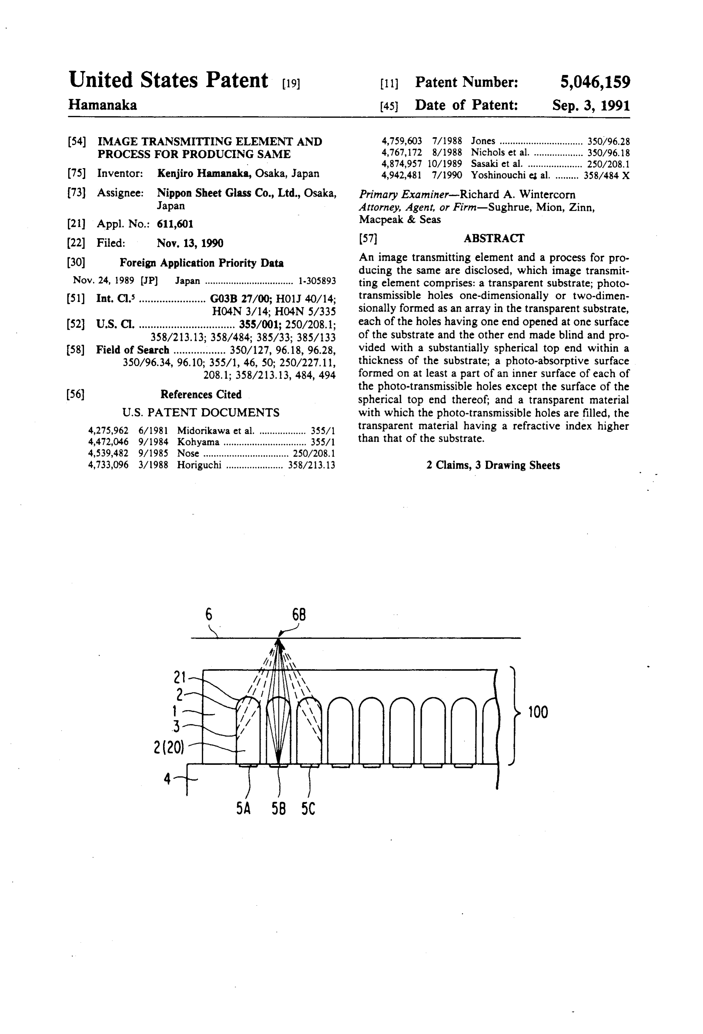
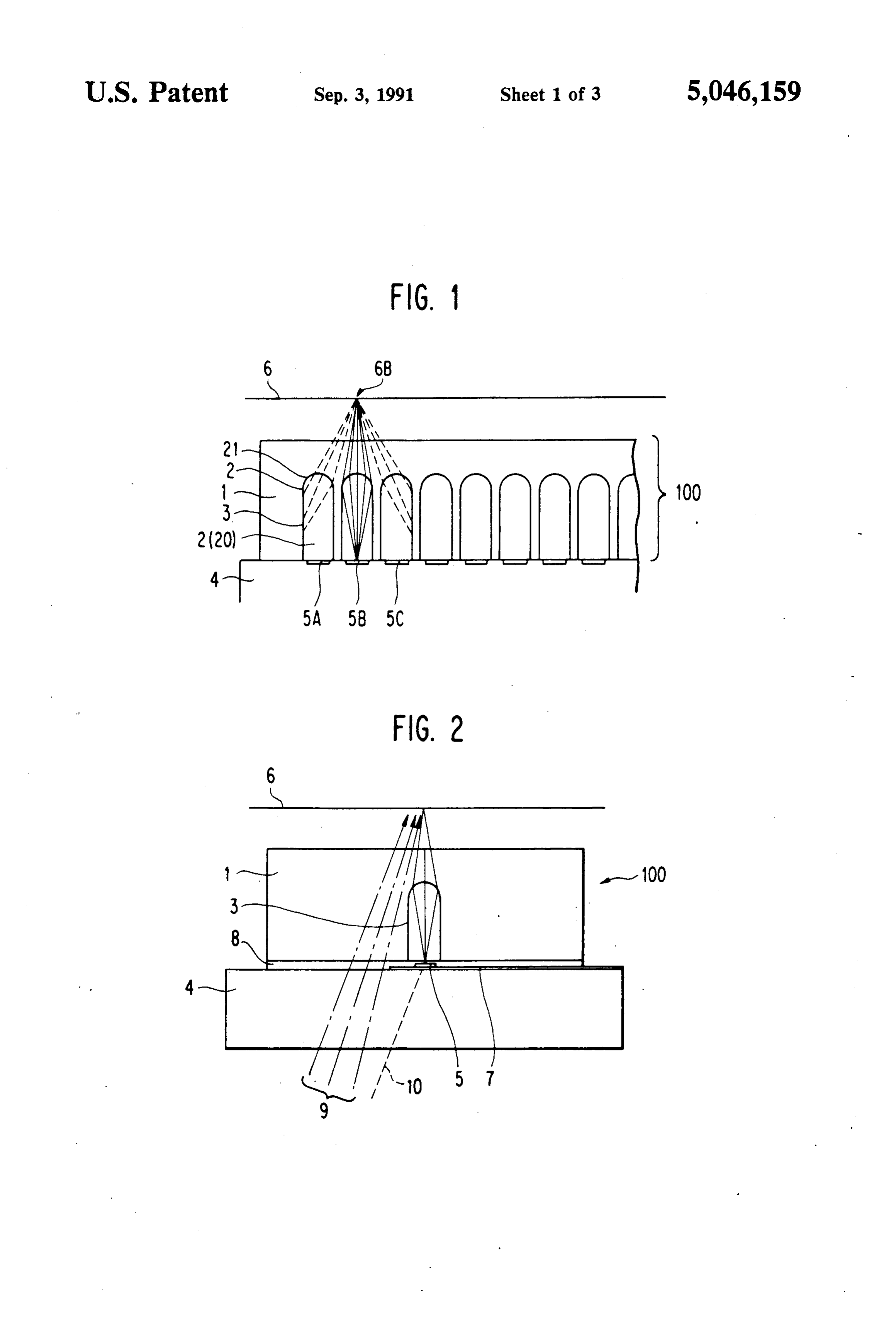
FIG. 1 is a vertical section showing the image trans 5 that the holes 2 and the sensor elements 5 are arranged mitting element according to one embodiment of the so as to have one-to-one correspondence.
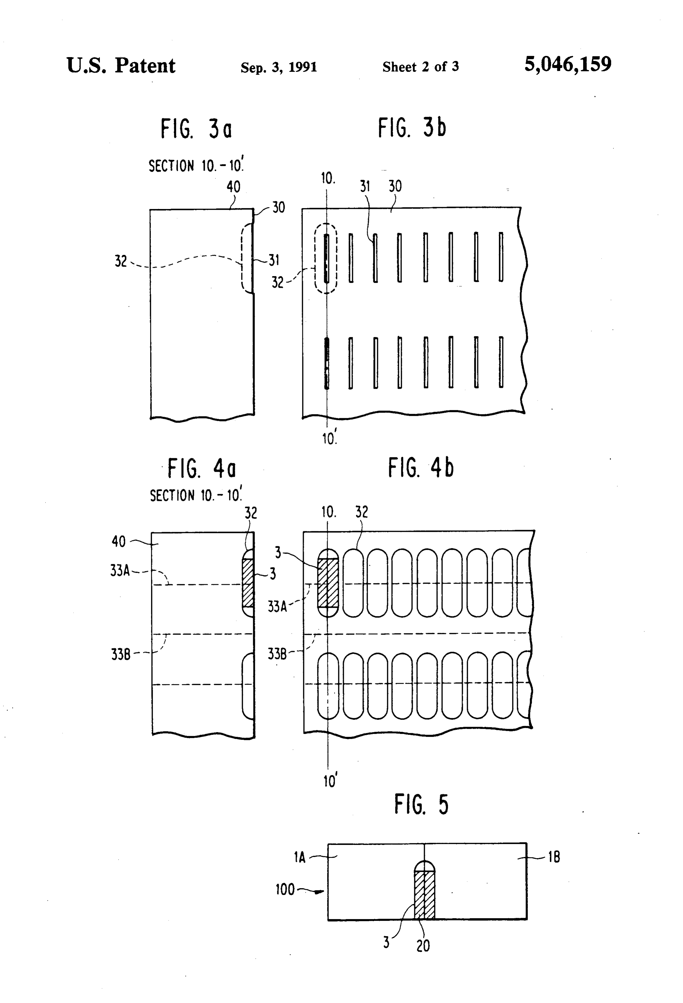
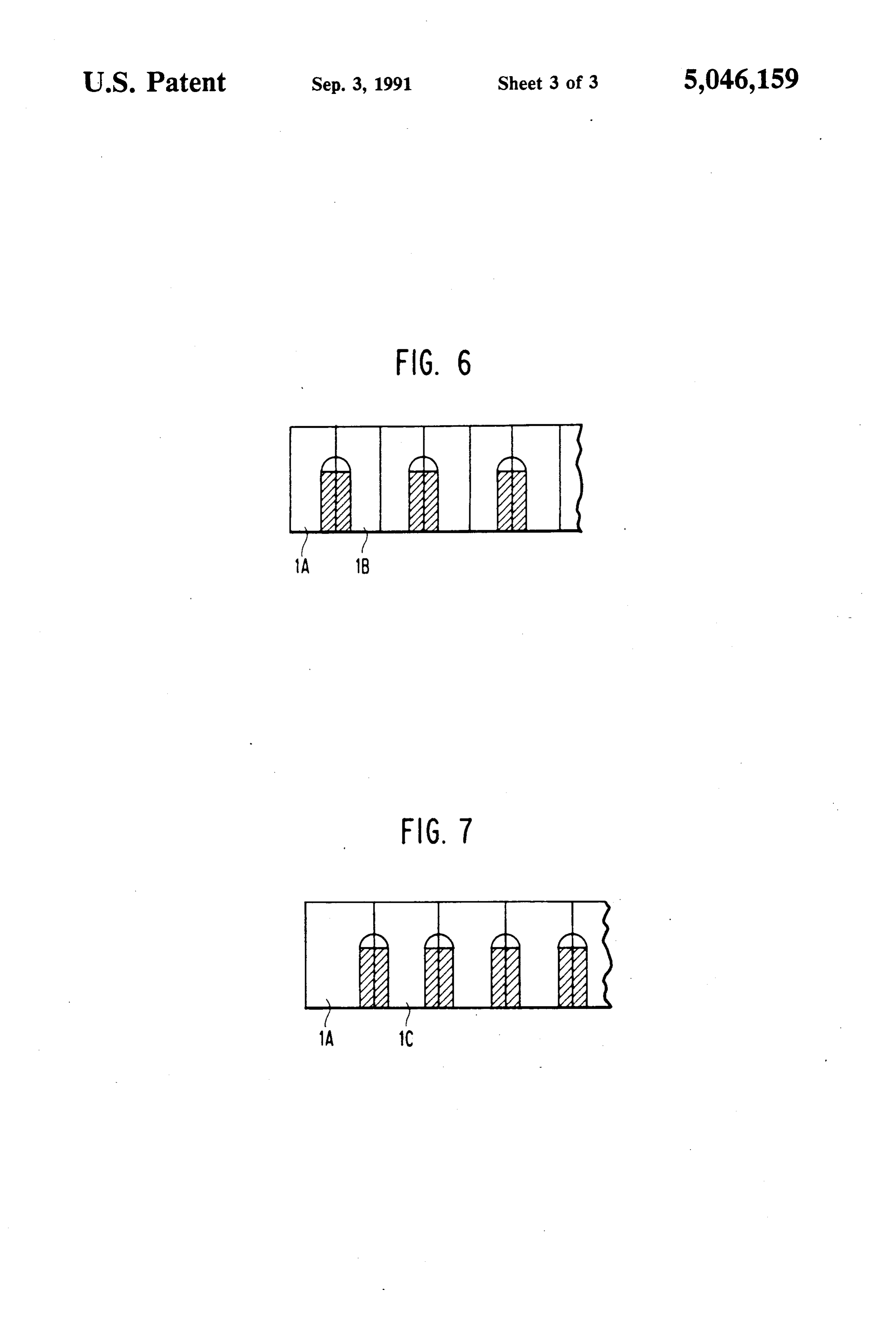
present invention; The contact sensor 4 is formed in a manner so that FIG. 2 is a cross section of the image transmitting almost one half area of the surface of a transparent element shown in FIG. 1; substrate is covered with a photo-shield layer 7 and FIGS. 3 through 5 are views for explaining one em 10 sensor elements 5 are one-dimensionally arrayed on the bodiment of the process for producing an image trans upper surface of and near the inner side edge of the mitting element according to the present invention, in photo-shield layer 7.
which FIG. 3 is a plan view and a transversal section An illuminating light source is disposed at the back showing the state in which a mask film having an array side of the contact sensor 4 so that the original docu of slit openings for etching is formed on a substrate, 15 ment surface 6 is irradiated with illuminating light 9 FIG. 4 is a plan view and a transversal view showing through a not-photo-shield portion of the sensor sub the state of the substrate after etching, and FIG. 5 is a State.
sectional view showing an image transmitting element At this time, light rays 10 toward the sensor element obtained by joining a pair of substrates each having 5 are grooves to each other and then cutting the joined body 20 Thecut by the photo-shield layer 7. light reflected from the original document sur of the substrates; face 6 (rays illustrated by solid lines in FIGS. 1 and 2) is FIG. 6 is view for explaining one embodiment of the incident into the photo-transmissible hole through the image transmitting element according to the present corresponding spherical top ends 21 and then focusedly invention in which the photo-transmissible holes are incident into the corresponding sensor elements 5A, 5B, formed two-dimensionally; and 25
FIG. 7 is view for explaining another embodiment of 5C, etc. of the contact sensor. the image transmitting element according to the present At this time, since the interior of each of the photo invention in which the photo-transmissible holes are transmissible holes 2 is filled with the transparent mate formed two-dimensionally. rial 20 having a refractive index higher than that of the 30 substrate 1, the spherical top end 21 of each of the holes
DETAILED DESCRIPTION OF PREFERRED 2 functions as a convex lens. EMBODIMENT The incident light is bent inwards owing to the con Referring to the drawings, an embodiment of the vex lens effect so as to be incident effectively into each image transmitting element according to the present of the sensor elements 5A, 5B, 5C, etc. On the other invention will be described hereunder. 35 hand, the light obliquely reflected and scattered from FIGS. 1 and 2 are a vertical section and a cross sec the original document surface 6 in the oblique direction tion respectively which show an example in which an (rays illustrated by dotted lines in FIG. 1) is indeed image transmitting element 100 according to the present incident into the adjacent photo-transmissible holes 2, invention is combined with a contact type image sensor which are not corresponding holes, but the inner walls 4 (hereinafter referred to as "contact sensor") so as to 40 of the photo-transmissible holes 2 have the photo constitute an apparatus for detecting one-dimensional absorptive surface 3, so that the obliquely reflected and image information on an original document surface 6. scattered light cannot reach any of the sensor elements The image transmitting element 100 is arranged such 5 of the contact sensor 4.
that a number of substantially cylindrical photo-trans That is, the light (the rays illustrated by the solid lines missible holes whose end portions have a focusing func 45 in FIGS. 1 and 2) which is reflected from each of the tion are formed one-dimensionally at predetermined very small area on the original document surface posi intervals in the thickness of a transparent substrate 1 tioned just above the corresponding sensor element 5, made of, for example, a glass (e.g., alkali-free glass, for example, from an area 6B just above the sensor quartz glass, soda-line glass) or plastic (e.g., UV or heat element 5B in FIG. 1, is incident into the corresponding curable acrylic resins, polymethyl methacrylate, poly 50 sensor element 5 efficiently through the lens effect of carbonate) having a flat surface. the spherical top end 21 of the corresponding photo The photo-transmissible holes 2 each having a very transmissible hole 2.
small diameter is provided in the substrate in such a Consequently, respective points in a one-dimensional manner that one end opens on one surface side of the area on the original document surface 6 have one-to-one substrate 1, and the other blind end which is made so as 55 correspondence to the respective sensor elements of the not to penetrate through the substrate but is stopped contact sensor 4 so as to realize clear one-dimensional while leaving a small thickness of the substrate. A top image transmission with no cross talk light leaking to end 21 of each of the holes 2 is formed so as to be sub adjacent picture elements.
stantially spherical, a photo-absorptive coating film 3 of Although a wiring pattern, a switching transistor a black paint is formed on at least a part of an inner side 60 (TFT), a surface protecting coating, etc. are provided surface of each of the holes 2 except the spherical top on the surface of the contact sensor 4, those parts have end 21 thereof, and the interiors of the holes 2 is filled no direct relation with the present invention and there with a transparent material 20 such as transparent resin fore they are omitted in FIGS. 1 and 2 for the sake of (e.g., light or heat curable acrylic resins, epoxy resins) simplification.
or the like having a refractive index higher than that of 65 Referring to FIGS. 3 through 5, a preferred embodi the substrate 1. ment of the process for producing the image transmit The photo-transmissible holes 2 are previously ting element according to the present invention will be formed at predetermined intervals corresponding to the described hereunder.
Page 7
First, as shown in FIG. 3, a surface of a transparent cut surfaces of the joined substrate may be mirror-pol glass substrate 40 is coated with a mask film 30 com ished so as to improve the smoothness of the surfaces, or posed of a material such as Cr which is anti-corrosive the cut surfaces may be coated with a transparent coat against a glass etching liquid to be used in a later etchinging film such as a sol-gel film, a resin film, or the like, so step. A number of rows each having a number of elon as to make the surfaces smooth, without performing gated slit openings 31 are formed in the mask film 30 at mirror-polishing.
predetermined intervals by use of a well-known photo In the case where the image transmitting element 100 lithographic process. The number of elongated slit is integrally bonded to the contact sensor 4 for use, it is openings 31 is one-directionally formed at predeter preferred that the thermal expansion coefficients of the mined intervals the same as those of the photo-trans 10 substrate materials of the image transmitting element missible holes 2. 100 and the contact sensor 4 are the same as or substan An end portion of each of the slit openings is made tially the same as each other.
blind so as to stop in the inside of the side edge of the For example, if the contact sensor 4 is made of #7059 substrate 40. glass (a trademark of Corning Co.) or quartz glass as its By immersing the above-mentioned glass substrate 15 substrate, it is preferred that the same material is se having the mask film into a glass etching liquid having lected as the substrate material of the image transmit a main component such as fluoric acid, etching starts ting element 100.
from the slit openings 31 in the mask film so that the However, if high accuracy is not necessary, a trans glass substrate 40 is etched substantially isotropically parent resin material (e.g., UV or heat curable acrylic from the surface of the glass substrate into the interior resin, polymethyl methacrylate, polycarbonate) may be thereof and grooves 32 each having substantially semi is used as the image transmitting element 100. spherical opposite ends and a substantially semi-cylin It is not always necessary to coat the whole length of drical middle portion are obtained as illustrated by the photo-transmissible holes 2 with the photo-absorptive dotted lines in FIG. 3.
Next, after the mask film 30 has been removed by 25 coating film 3, and, for example, there is a case where it etching, the middle portion of the inner wall surface of 60% to 80% ifofonly is sufficient the the area of the length about from whole length of the holes is coated.
each of the grooves 32 except the opposite semi-spheri It is not always necessary that the top end 21 having cal portions is coated with a black paint so as to form the light focusing function of the photo-transmissible the photo-absorptive coating film 3. holes accurately semi-spherical so long as the top end 21 In order to coat the black paint on the limited specific has the effect for bending light inward of the photo area as described above, for example, a photo resist is transmissible hole by refraction. That is, the provided with a pattern by a conventional photo lithog may be a shape of curved surface constitutingtopa part end 21 raphy technique, then the whole of the surface is coated a sphere, a paraboloid of revolution, a hyperboloid of of with the black paint, and then the photo resist is re moved so as to leave the black paint only at the neces 35 revolution,
Zoid.
or the like, or a polyhedron such as a trape sary portions.
A pair of grooved substrates produced in such a man Although FIGS. 1 and 2 show that the top end 21 ner as described above is made to be opposite to each accurately focus an original document surface onto a other so that the grooves 32 of one of the grooved sensor element of a contact sensor, it is sufficient if substrates are made to accord with the corresponding 40 reflected light from the original document surface is incident into the area of the sensor element.
grooves 32 of the other of the grooved substrates. The The image transmitting element according to the pair of grooved substrates is made accurately accord in .
position with each other and bonded to each other by present invention in which the photo-transmissible using an adhesive agent. The adhesive agent is transpar holes are formed two-dimensionally as an array can be ent after being hardened and has a refractive index 45 produced in the manner described in FIGS. 6 and 7 but is not restricted thereto.
higher than that of the substrate 40.
At this time, the grooves 32 are filled with the adhe In one embodiment shown in FIG. 6, a number of sive agent before bonding so that the adhesive agent image transmitting element each composed of a pair of becomes the transparent material 20 filled in the photo members 1A and 1B produced by the above-described transmissible holes 2 in the image transmitting element SO process are stacked along the longitudinal direction 100. After the adhesive agent has been hardened, the thereof to form a two-dimensional array of the photo joined body is cut along a cutting line 33A perpendicu transmissible holes.
lar to the row of grooves at a longitudinally central In another embodiment shown in FIG. 7, the image position of the grooves and also along a cutting line 33B transmitting element is composed of a member having dividing the groove row. 55 grooves on one surface thereof 1A and a number of Each of elongated pieces cut through the method members each having grooves on both surfaces thereof described above is the image transmitting element 100 1C. In this embodiment, the intervals of the photo-trans according to the present invention. mitting holes can be reduced in comparison to the em Although one embodiment has been described above, bodiment shown in FIG. 6.
the present invention is not limited to the above embodi 60 Although the case where the image transmitting ele ment but various modifications are possible. For exam ment 100 according to the present invention is com ple, it is possible that each of the grooves 32 of a pair of bined with the contact sensor has been described in the substrates is previously filled with a transparent mate above embodiment, the image transmitting element 100 rial having a high refractive index (e.g., glass, resins), may be combined with an LED array in place of the the surface of the filled transparent material is made flat 65 contact sensor to thereby constitute an optical system of by polishing, and then the pair of substrates are joined an LED printer or combined with a liquid crystal shut each other. Further, after the joined body of the sub ter array to thereby constitute an optical system of a strates is cut along the cutting lines 33A and 33B, the liquid crystal printer.
Page 8
By use of the image transmitting element according opened at one surface of said substrate and the to the present invention, it is possible to make an optical other end made blind and provided with a substan system such as a contact type image sensor, an LED tially spherical top end within a thickness of said printer and the like extremely small. For example, the substrate;
distance between an original document surface and a a photo-absorptive surface formed on at least a part of light sensor surface becomes about from 0.6 to 2.0 mm. an inner surface of each of said photo-transmissible At this time, even if there is a gap about not more holes except the surface of said spherical top end than 1 mm between the original document surface and thereof; and the image transmitting element, since light traveling in a transparent material with which said photo-trans the direction toward the adjacent picture elements is O missible holes are filled, said transparent material intercepted by the photo-absorptive surfaces of the having a refractive index higher than that of said inner walls of the respective photo-transmissible holes substrate.
in the image transmitting element, there is no fading of 2. A process for producing an image transmitting an image signal due to cross talk so that a clear image of element as in claim 1, comprising steps of: high resolution can be obtained. That is, there are ad 15 providing on one surface of each of a pair of transpar vantages that the depth of focus can be made compara ent substrates an anti-corrosive mask film; tively large and that the surface is hard to be injured forming an array of slit openings in parallel to each because of not-contact.
Moreover, although in a perfect contact type image other, the respective end portions of said slit open sensor, the size of illuminating light leading windows 20 ings being positioned in the inside of the side edge corresponding to respective picture elements cannot be of said substrate;
made large for the sake of keeping resolution so that the contacting an etching material to the surface of said transmitting efficiency of the illumination to an original substrate on which said mask film is provided so as document surface becomes low, there is not such a to etch the surface of said substrate isotropically limitation in the image transmitting element according 25 from said slit openings to thereby form an array of to the present invention, and for example, as shown in grooves each having substantially spherical oppo the embodiment in FIG. 2, it is possible to lead illumi site end surfaces;
nating light to an original document from the back side providing a photo-absorptive surface on at least a of the image transmitting element 100 and the contact part of an inner wall of each of said grooves except sensor 4 efficiently, so that it is possible to improve the 30 said spherical opposite end surfaces thereof; utilization efficiency of illumination. removing said mask film;
While the invention has been described in detail and filling said grooves with a transparent material hav with reference to specific examples thereof, it will be ing a refractive index higher than that of said sub apparent to one skilled in the art that various changes Strate;
and modifications can be made therein without depart 35 joining said pair of substrates each having said ing from the spirit and scope thereof. grooves to each other in a manner such that said WHAT IS CLAIMED IS: grooves of one of said pair of substrates are made to 1. An image transmitting element comprising: accord with said grooves of the other of said pair of a transparent substrate; substrate; and photo-transmissible holes one-dimensionally or two 40 cutting said joined body of said substrates at a posi dimensionally formed as an array in said transpar tion crossing said array of said grooves. ent substrate, each of said holes having one end k k ck k ck
Provenance
- Collection
- Cited prior art
- Original PDF
- patentimages.storage.googleapis.com →
- Filed
- 1990-11-13
- Pages
- 8
- Method
- pdftotext (the PDF's own text layer) + pdftoppm 300dpi page scans
- Source
- Google Patents bibliographic record
- Granted
- 1991-09-03
- Inventors
- Kenjiro Hamanaka; Nippon Sheet Glass Co Ltd
- Transcribed from
- patentimages.storage.googleapis.com →