patent · US4746618
Method of continuously forming an array of photovoltaic cells electrically connected in series
24 May 1988
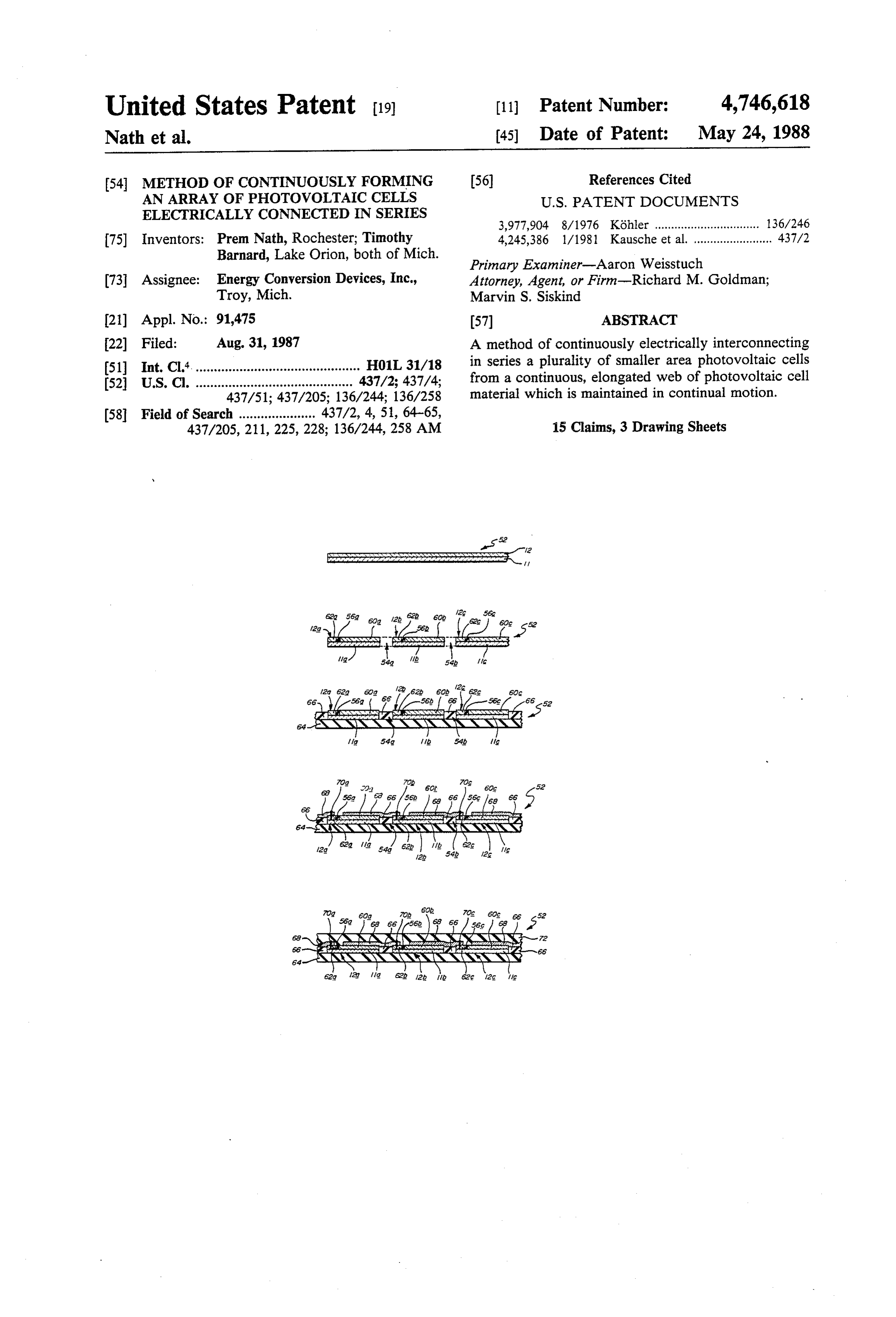
Page 1 — bibliographic record
United States Patent (19) 11 Patent Number: 4,746,618 Nath et al. (45) Date of Patent: May 24, 1988 54 METHOD OF CONTINUOUSLY FORMING (56) References Cited
AN ARRAY OF PHOTOVOLTAC CELLS
ELECTRICALLY CONNECTED IN SERIES U.S. PATENT DOCUMENTS 3,977,904 8/1976 Köhler ................................ 136/246 75) Inventors: Prem Nath, Rochester; Timothy 4,245,386 l/1981 Kausche et al. ........................ 437/2 Barnard, Lake Orion, both of Mich. Primary Examiner-Aaron Weisstuch 73 Assignee: Energy Conversion Devices, Inc., Attorney, Agent, or Firm-Richard M. Goldman; Troy, Mich. Marvin S. Siskind (21) Appl. No.: 91,475 (57) ABSTRACT 22 Filed: Aug. 31, 1987 A method of continuously electrically interconnecting 51) Int. Cl. ............................................. H01L 31/18 in series a plurality of smaller area photovoltaic cells 52 U.S. C. ........................................... 437/2; 437/4; from a continuous, elongated web of photovoltaic cell 437/51; 437/205; 136/244; 136/258 material which is maintained in continual motion.
58 Field of Search ..................... 437/2, 4, 51, 64-65, 437/205, 211, 225, 228; 136/244, 258 AM 15 Claims, 3 Drawing Sheets
YAYYYXXXYYES
Page 2
Drawing sheet — no readable text.
Page 3
Drawing sheet — no readable text.
Page 4
Drawing sheet — no readable text.
Page 5
assignee of the present invention. More specifically, the
METHOD OF CONTINUOUSLY FORMING AN assignee of the present invention is recognized as the ARRAY OF PHOTOVOLTAC CELLS world leader in photovoltaic technology. Photovoltaic ELECTRICALLY CONNECTED IN SERIES devices produced by said assignee have set world re cords for photoconversion efficiency and long term
FIELD OF THE INVENTION stability under operating conditions (the efficiency and This invention relates generally to methods of fabri stability considerations will be discussed in greater de cating relatively large area photovoltaic devices and tail hereinbelow). Additionally, said assignee has devel more particularly to a method of forming and electri oped commercial processes for the continuous roll-to cally interconnecting in series a plurality of photovol 10 roll manufacture of large area photovoltaic devices. taic cells from a moving web of photovoltaic cell mate In this roll-to-roll processing, a web of substrate ma rial. terial may be continuously advanced through a succes sion of operatively interconnected, environmentally
BACKGROUND OF THE INVENTION protected deposition chambers, wherein each chamber Owing to the increasing scarcity of non-renewable 15 is dedicated to the deposition of a specific layer of semi energy reserves such as coal, petroleum and uranium, it conductor alloy material onto the web or onto a previ is essential that increased use be made of alternative ously deposited layer. In making a photovoltaic device, non-depletable energy sources, such as photovoltaic for instance, of n-i-p type configuration, the first cham energy. Single crystal photovoltaic devices, especially 20 ber is dedicated for the deposition of a layer of an n-type crystalline silicon photovoltaic devices, have been uti semiconductor alloy material, the second chamber is lized for some time as sources of electrical power be dedicated for the deposition of a layer of substantially cause they are inherently non-polluting, silent and con intrinsic amorphous semiconductor alloy material, and sume no expendable natural resources in their opera the third chamber is dedicated for the deposition of a tion. However, the utility of such crystalline devices has layer of a p-type semiconductor alloy material. The been limited by problems associated with the manufac 25 layers of semiconductor alloy material thus deposited in ture thereof. More particularly, single crystalline mate the vacuum envelope of the deposition apparatus may rials are: (1) difficult to produce in sizes substantially be utilized to form photoresponsive devices, such as, larger than several inches in diameter, (2) thicker and but not limited to, photovoltaic devices which include heavier than their thin film counterparts; (3) fragile and 30 one or more cascaded n-i-p type cells. By making multi therefore susceptible to breakage; and (4) expensive and ple passes through the succession of deposition cham time consuming to fabricate.
Recently, considerable effort has been expended to bers, or bychambers, providing one or more additional triads of develop systems and processes for preparing thin film deposition configurations may multiple stacked cells of various be obtained. Note, that as used amorphous semiconductor alloy materials which en compass relatively large areas and which can be depos 35 herein, the term "n-i-p type' will refer to any sequence ited so as to form p-type and n-type semiconductor of n and p or n, i and players of semiconductor alloy material operatively disposed and successively depos alloy layers for the production therefrom of thin film ited to form a photoactive region wherein charge carri photovoltaic devices which are substantially equivalent ers are or superior to their crystalline counterparts in operation incidentgenerated radiation.
by the absorption of photons from and efficiency. It should be noted at this point that the 40
The concept of utilizing multiple stacked cells, to term "amorphous' as used herein, is defined to include enhance photovoltaic device efficiency has been known alloys or materials exhibiting long range disorder, al since at least as early as 1955. Essentially, the concept though said alloys or materials may exhibit short or employs different band gap devices to more efficiently intermediate range order or even contain crystalline inclusions. Also, as used herein, the term "microcrystal 45 collect various portions of the solar spectrum and line' is defined as a unique class of said amorphous thereby increase open circuit voltage (Voc). The tan materials characterized by a volume fraction of crystal dem cell device (by definition) incorporates two or line inclusions, said volume fraction of inclusions being more stacked cells with the light directed serially greater than a threshold value at which the onset of through each cell. In the first cell, a large band gap semiconductor alloy material absorbs only the short substantial changes in certain key parameters such as 50 wavelength electrical conductivity, band gap and absorption con light, while in subsequent cells, smaller stant occur. It is to be noted that pursuant to the forego band gap semiconductor alloy materials are employed ing definitions, the microcrystalline, p-doped, wide to absorb the longer wavelengths of light which pass band gap, semiconductor alloy material, referred to through the first cell. By substantially matching the herein, falls within the generic term "amorphous'. 55 photogenerated currents from each cell of the tandem As mentioned hereinabove, amorphous thin film arrangement, the overall open circuit voltage becomes semiconductor alloys have gained acceptance for the the sum of the open circuit voltage of each cell, while fabrication of photovoltaic cells therefrom. This is be the short circuit current thereof remains substantially cause the amorphous thin film semiconductor alloys (1) constant. Such tandem cell structures can be relatively can now be manufactured by relatively low cost contin economically fabricated in large areas by employing uous processes, (2) possess a wide range of controllable thin film amorphous, semiconductor alloy materials electrical, optical, and structural properties and (3) can (with or without crystalline inclusions). It should be be deposited to cover relatively large areas. Among the noted that when crystalline semiconductor materials are semiconductor alloy materials exhibiting the greatest employed for the fabrication of stacked cell structures, present commercial significance are amorphous silicon, 65 it is virtually impossible to match the lattice constants of amorphous germanium and amorphous silicon-ger the different crystalline materials thereof. Therefore, it manium based alloys. Such alloys have been the subject is not possible to fabricate such crystalline tandem cell of a continuing development effort on the part of the structures in a commercially feasible manner. In con
Page 6
trast thereto, and as the assignee of the instant invention each said slit extending through the semiconductor has shown, such tandem cell structures are not only alloy material and the substrate. The slit is of a length possible, but can be economically fabricated over large selected to include a non-slitted connector between areas by employing the amorphous seniconductor alloy each terminus of said slit and the edge of said cell proxi materials and the deposition techniques discussed and mate thereto so that said non-slitted connectors prevent briefly described herein. the division of said elongated photovoltaic cell into a More particularly, the assignee of the instant inven plurality of discrete smaller area photovoltaic cells. tion is presently able to manufacture stacked, large area Electrical communication is then established between photovoltaic devices on a commercial basis by utilizing said adjacent smaller area cells which are disposed on the previously referenced, continuous deposition, roll 10 opposite sides of said slit. Only at this time are said to-roll processor. That processor is characterized as a connectors severed so that said elongated cell is con 1.5 megawatt capacity machine insofar as its annual verted into an elongated array of discrete smaller area output of photovoltaic devices is capable of producing photovoltaic cells which are electrically interconnected 1.5 megawatts of electrical power. Said 1.5 megawatt in series.
processor, as presently configured, is adapted to pro 15 The method may further include the steps of electri duce tandem photovoltaic cells which comprise two cally isolating a minor portion of the surface area of stacked n-i-p type photovoltaic devices disposed opti each discrete photovoltaic cell from the remainder of cally and electrically in series upon a stainless steel the surface area of each discrete cell by either forming substrate. The processor currently includes six opera grooves through the layers of semiconductor alloy ma tively interconnected, dedicated deposition chambers, 20 terial deposited upon the continuous substrate or by each deposition chamber adapted to sequentially de removing a stripe therefrom, which stripe includes posit one of the layers of semiconductor alloy material those layers of semiconductor alloy material. These from which the tandem device is fabricated. grooves are adapted to expose the subjacent electrically Despite the fact that non-polluting, non-depletable conductive substrate for effecting electrical communi photovoltaic energy is so attractive and despite the fact 25 cation between adjacent small area cells. that Applicants' assignee has been able to develop pro At this point, the slits are filled with electrically insu duction apparatus in which thin film photovoltaic de lating material so that adjacent smaller area photovol vices can be manufactured in a continuous roll-to-roll taic cells are electrically isolated from one another. In process, the cost in dollars per peak watt of power the event that an electrically conductive substrate is generated by thin film photovoltaic devices remains too 30 used, the back surface of the substrate is laminated with high to be cost competitive with conventional energy an electrically insulating encapsulating material prior to sources. One reason for this relatively high cost is that insulating the slitted space between adjacent cells with while the aforementioned continuous roll-to-roll manu the electrically insulating material. In those instances in facture of thin film photovoltaic devices has reduced which an electrically insulating substrate is utilized, a the deposition expense as compared to the expense of 35 continuous layer of electrically conductive material is batch depositing those devices, in order to series con deposited upon said insulating substrate prior to slitting nect discrete devices, it has heretofore been necessary said continuous photovoltaic cell into the plurality of to sever said devices from the web and then electrically smaller area cells and the slitted space between adjacent and mechanically reconnect the severed devices in said cells is insulated with an electrically insulating material. series relationship. The processing steps involved in the 40 The electrically isolated adjacent cells are then electri severing of discrete devices, electrically interconnect cally interconnected across said insulated slit by form ing in series those severed devices, and mechanically ing a plurality of electrically conductive grid lines reconnecting the severed, electrically interconnected which extend from said major portion of said surface devices could not be accomplished in roll-to-roll fash area of one discrete cell to said minor portion of said ion, was labor intensive, time consuming and hence, 45 surface area of said adjacent discrete cell, whereby the expensive. upper surface of each smaller area cell is electrically It is therefore the principle object of the subject in interconnected in series to the lower electrode surface vention to provide a continuous, roll-to-roll process for of said adjacent cell. In another embodiment of electri electrically interconnecting in series a plurality of dis cally interconnecting adjacent cells is the step of form crete small area photovoltaic cells, which process is 50 ing at least one bus bar which electrically interconnects simple and cost effective. the plurality of grid lines of one cell to the substrate This and other objects and advantages of the subject electrode of the adjacent cell.
invention will become apparent from a perusal of the It may thus be seen that in the aforementioned man drawings, the detailed description of those drawings, ner, a plurality of discrete smaller area cells may be and the claims which follow. 55 electrically interconnected in series so as to obtain a BRIEF SUMMARY OF THE INVENTION desired voltage therefrom. Finally, the upper surface of the discrete electrically interconnected photovoltaic
There is disclosed herein a method of continuously smaller area cells are encapsulated with an electrically electrically interconnecting in series an array of photo isolating laminate material.
voltaic cells, said method including the steps of provid 60 In its broadest form, there is described herein an ing an elongated web of continuous photovoltaic cell improved method of electrically interconnecting in material, which continuous cell material comprises a Series an array of photovoltaic cells in which successive continuous substrate upon which continuous thin film continuous layers of semiconductor alloy material are layers of semiconductor alloy material are disposed. It is deposited onto an elongated web of substrate material important for purposes of cost reduction that the photo 65 so as to form an elongated web of continuous photovol Voltaic cell material be continuously moved through taic cell material. This method includes the specific processing stations to a take-up station. In its path of steps of forming a plurality of discrete smaller area travel, at least one slit is formed in said elongated cell, photovoltaic cells from the single cell and electrically
Page 7
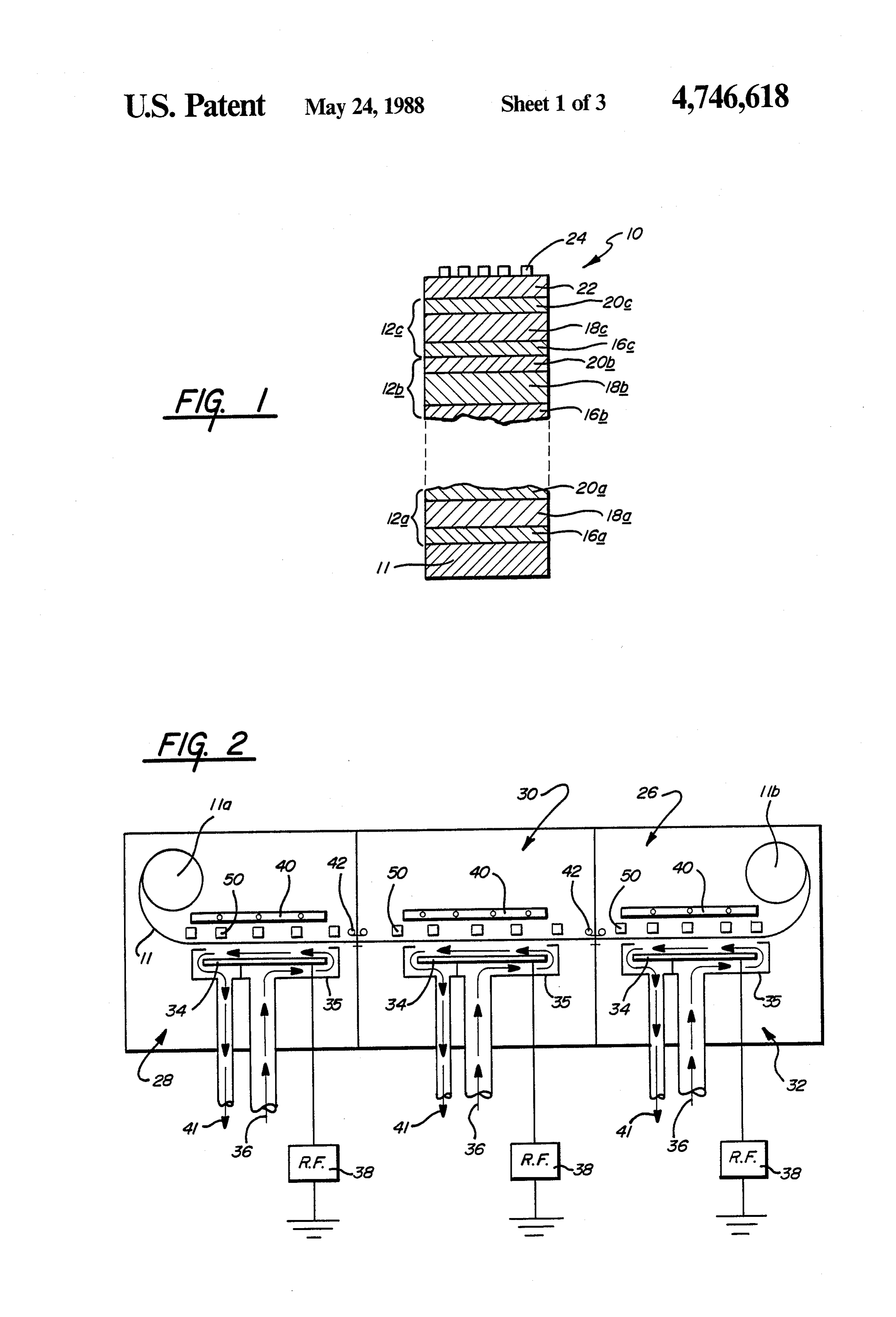
interconnecting those discrete cells in series while main DETAILED DESCRIPTION OF THE taining the web in continuous motion. According to this DRAWINGS method, at least one slit is formed in said elongated cell so as to extend through the semiconductor alloy mate 5 Referring I. The Photovoltaic Cell now to the drawings and particularly to rial and the substrate, said slit being of a length which FIG. 1, a photovoltaic leaves a non-slitted connector between each terminus of cell, formed of a plurality of said slit and the edge of said cell proximate thereto. successively deposited n-i-players, each of which in cludes, preferably, a substantially amorphous thin film
Again, the electrical communication is preferably semiconductor alloy material is shown generally by the formed between the cells which are disposed on oppo 10 reference numeral 10.
site sides of said slits. The fabrication may be completed by encapsulating both sides of the photovoltaic cell voltaic device, such asFIG.
More particularly, 1 shows an n-i-p type photo material and by severing the number of discrete cells ual n-i-p type cells 12a, 12b andcell, a solar made up of individ 12c. Below the lower from the web which will provide the preselected volt most cell 12a is a substrate 11 which may be formed of age. 15 a transparent glass or synthetic polymeric member; or BRIEF DESCRIPTION OF THE DRAWINGS formed from a metallic material such as stainless steel, aluminum, tantalum, molybdenum, chrome; or formed
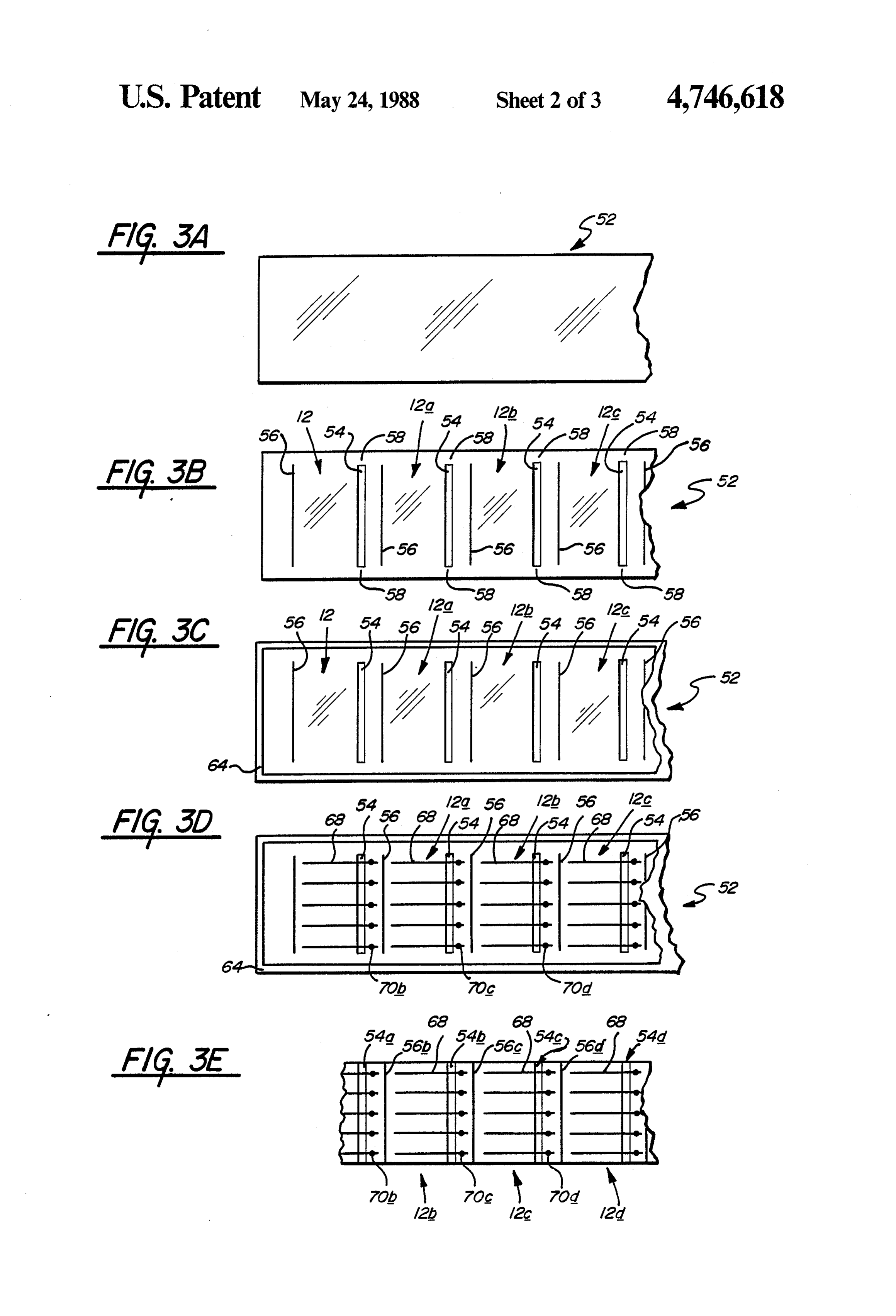
FIG. 1 is a fragmentary, cross-sectional view of a from metallic particles embedded within an insulator. tandem photovoltaic device of the type which may be Although certain applications may require the deposi employed in the practice of the instant invention, said 20 tion of a thin oxide layer and/or a series of base contacts device comprising a plurality of stacked n-i-p type pho prior to the deposition of semiconductor alloy material, tovoltaic cells; the term "substrate' shall include not only a flexible FIG. 2 is a schematic view of a multiple chamber film, but also any elements added thereto by prelimi deposition apparatus of the type which may be em nary processing. Also included within the scope of the ployed for the fabrication of the tandem photovoltaic 25 present invention are substrates formed of synthetic cells illustrated in FIG. 1; polymers and, metals coated with a synthetic polymer FIG. 3A is a partial top plan view illustrating a con to which one or more conductive base electrodes are tinuous web of photovoltaic cell material of the type applied.
depicted in FIG. 1; Each of the cells 12a, 12b and 12c is preferably fabri FIG. 3B is a partial top plan view illustrating the 30 cated with a thin film semiconductor body containing at continuous web of photovoltaic cell material of FIG. least a silicon or silicon:germanium alloy. Each of the 3A with a plurality of slits cut thereinto and a substrate semiconductor bodies includes a p-type conductivity exposing groove formed in each of the cells thereof; semiconductor layer 20a, 20b or 20c, a substantially FIG. 3C is a partial plan view illustrating the continu intrinsic semiconductor layer 18a, 18b or 18c, and an ous web of photovoltaic cell material of FIG. 3B with 35 n-type conductivity semiconductor layer 16a, 16b or an encapsulant applied to the rear surface thereof and 16c. Note that the intrinsic layer may include traces of the slits filled with an electrically insulating material; n-type or p-type dopant material without forfeiting its FIG. 3D is a top plan view illustrating the continuous characteristic neutrality, hence it may be referred to web of photovoltaic cell material of FIG. 3C with the herein as a "substantially intrinsic layer'. As illustrated, addition thereto of an electrically interconnecting grid 40 cell 12b is an intermediate cell and, as indicated in FIG. extending across the slitted space between discrete 1, additional intermediate cells may be stacked atop the cells; illustrated cells without departing from the spirit or FIG.3E is a top plan view illustrating the continuous cell scope of the present invention. Similarly, the tandem web of photovoltaic cell material of FIG. 3D as that 45 n-i-pmay include only two stacked cells. Also, although photovoltaic cells are illustrated, this invention web is severed to form a plurality of discrete, electri may be advantageously practiced with differently con cally interconnected smaller area photovoltaic cells;
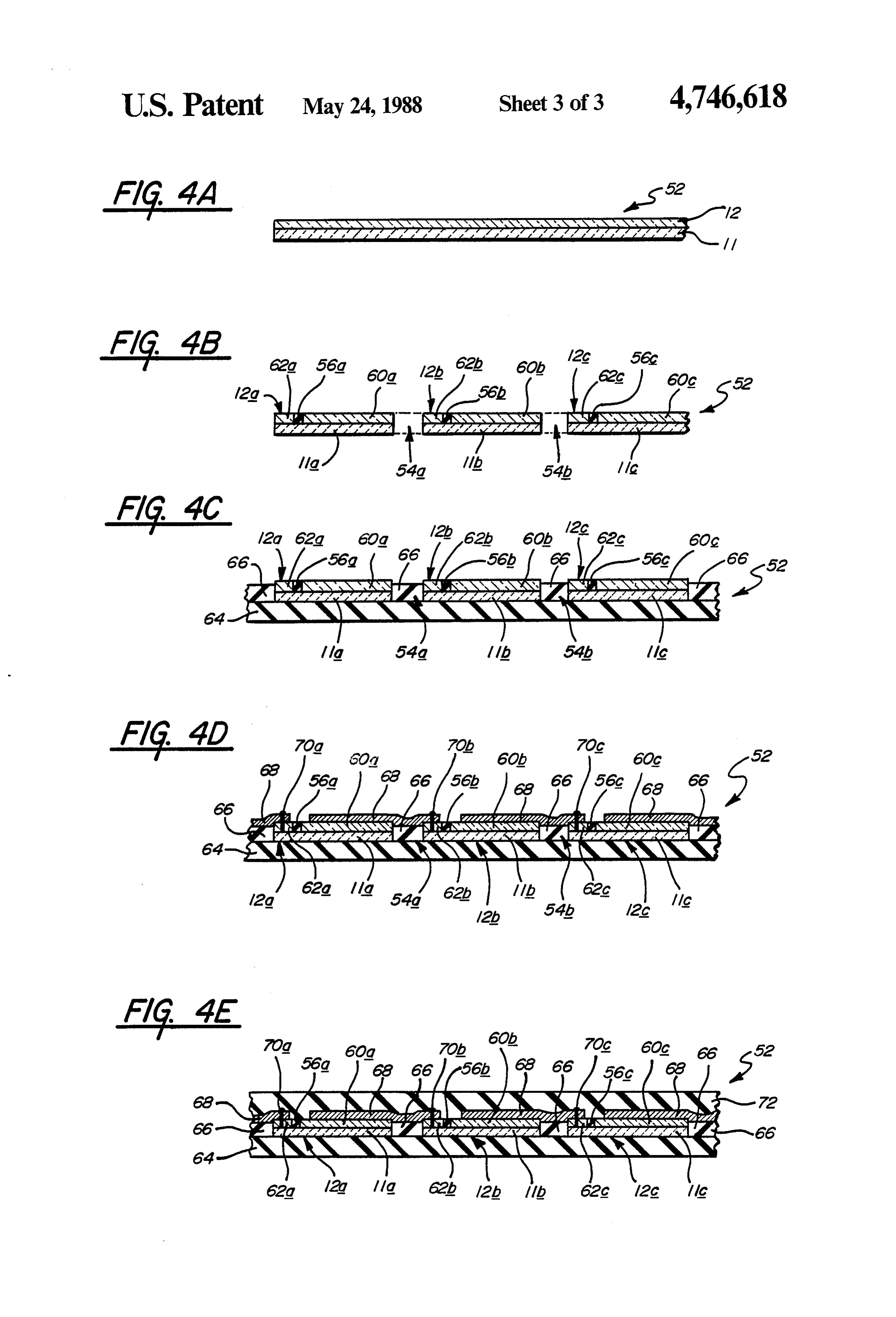
FIG. 4A is a partial cross-sectional view illustrating p-i-n cells, Schottky barrierincluding figured photovoltaic cells cells, single or multiple p-n cells as well as the continuous web of photovoltaic cell material of with any other semiconductor device having an appro
FIG. 3A;
FIG. 4B is a partial cross-sectional view illustrating 5 herein is meant to include any aggregation of n,asi and 0 priate top electrode. The term "n-i-p type' used the continuous web of photovoltaic cell material of layers operatively disposed to provide a photoactivep FIG. 3B with the slits cut between discrete cells and the region for generating charge carriers in response to the isolation grooves formed in the semiconductor alloy absorption of photon energy.
material thereof; 55 It is to be understood that following the deposition of FIG. 4C is a partial cross-sectional view illustrating the layers of semiconductor alloy material, a further the continuous web of photovoltaic cell material of deposition process may be either performed in a sepa FIG. 3C with the electrically insulating material pro rate environment or as a part of a continuous process. In vided between adjacent cells and the rear surface this step, a TCO (transparent conductive oxide) layer thereof having a laminate disposed thereover; 60 22, preferably formed of a material such as tin oxide, FIG. 4D is a partial cross-sectional view of the con indium oxide, indium tin oxide, zinc oxide, cadmium tinuous web of photovoltaic cell material of FIG. 3D stannate or combinations thereof is added atop the p illustrating the electrically interconnecting grid which layer 20c of the top most cell 12c, to function as the top extends across the insulated slit and separating adjacent electrode of the cell 10. An electrode grid 24 may be cells; and 65 added to the device where the cell is of a sufficiently FIG. 4E is a partial cross-sectional view illustrating large area, or if the conductivity of the TCO layer 22 is the continuous web of photovoltaic cell material of insufficient to obtain efficient collection of photogene FIG. 3E with an upper encapsulant added thereupon. rated current. The grid 24 is adapted to shorten the
Page 8
carrier path and increase the conduction efficiency. As a process gas supply conduit 36; a radio frequency gen discussed previously, the intrinsic layers 18a, 18b and erator or other source of electromagnetic power 38; a 18c of the respective cells 12a, 12b and 12c may be and process gas and plasma evacuation conduit 41; a plural preferably are formed from semiconductor alloy materi ity of transversely extending magnetic elements 50; a als having different band-gaps. For example, intrinsic plurality of radiant heating elements shown schemati layer 18c of cell 12c may have a band gap of approxi cally as 40 in FIG. 2; and a gas gate 42 operatively mately 1.7 eV, intrinsic layer 18b of cell 12b may have interconnecting the intrinsic deposition chamber to a band gap of approximately 1.5 eV and intrinsic layer each adjacent dopant chamber. 18a of cell 12a may have a band gap of approximately The supply conduits 36 are operatively associated 1.3 eV. In this manner, the most efficient use may be O with the respective cathodes 34 and other decomposi made of a large portion of the incident solar spectrum. tion mechanisms to deliver process gas mixtures to the II. The Multiple Glow Discharge Deposition Cham plasma, or other decomposition regions created in each bers deposition chamber between said decomposition mech Turning now to FIG. 2, a diagrammatic representa anism and the substrate 11. The cathode shields 35 are tion of multiple glow discharge chamber deposition 15 adapted to operate in conjunction with the web of sub apparatus for the continuous production of photovol strate material 11 and the evacuation conduit 41 to taic cells is generally illustrated by the reference nu confine the process gases within the cathode region of meral 26. The apparatus 26 includes a plurality of iso the deposition chambers.
lated, dedicated deposition chambers, each chamber of The radio frequency or other similar type of power which is interconnected by a gas gate 42 through which generator 38 operates in conjunction with the cathodes (1) sweep gases, and (2) a web of substrate material 11 34, the radiant heaters 40 and the grounded substrate 11 are adapted to unidirectionally pass. It is in an apparatus to form the plasma by disassociating and recombining of this type that photovoltaic cells similar to the cell 10 the elemental reaction gases entering the deposition of FIG. 1, may be readily manufactured. chambers into deposition species and compounds. The apparatus 26 is adapted to mass deposit amor 25 These species and compounds are then deposited onto phous semiconductor layers of n-i-p configuration onto the bottom surface of the substrate 11 as semiconductor the surface of the web of substrate material 11 which is layers. The substrate 11 is maintained substantially flat continually fed therethrough. To deposit the semicon by the plurality of rows of magnetic elements 50 which ductor layers required for producing multiple n-i-p type provide an attractive force urging the substrate 11 up cells, the apparatus 26 includes at least one triad of 30 wardly, out of its normal sagging path of travel. To deposition chambers. Each triad of deposition chambers form the photovoltaic cell 10 illustrated in FIG. 1, an comprises: a first deposition chamber 28 in which a n-type substantially amorphous layer of semiconductor layer of n-type conductivity semiconductor alloy mate alloy material is deposited onto the substrate 11 in the rial is deposited onto the deposition surface of the sub dopant deposition chamber 28, a layer of substantially strate 11 as the substrate 11 passes therethrough; a sec 35 intrinsic amorphous semiconductor alloy material is ond deposition chamber 30 in which a layer of intrinsic deposited atop the n-type layer in the deposition cham semiconductor alloy material is deposited atop the p ber 30 and a p-type substantially amorphous layer of type layer on the deposition surface of the substrate 11 semiconductor alloy material is deposited atop the in as the substrate 11 passes therethrough; and a third trinsic layer in the deposition chamber 32. As a result, in deposition chamber 32 in which a layer of p-type semi 40 the preferred embodiment, the apparatus 26 deposits at conductor alloy material is deposited atop the intrinsic least three amorphous semiconductor layers onto the layer on the deposition surface of the substrate 11 as the substrate 11 with the intrinsic layer deposited in deposi substrate 11 passes therethrough. It should be apparent tion chamber 30 differing in composition from the lay that (1) although only one triad of deposition chambers ers deposited in deposition chamber 28 and 32 by the has been illustrated, additional triads or additional indi 45 absence of at least one element which will be referred to vidual chambers may be added to the apparatus to pro as the dopant or doping species.
vide the machine with the capability of producing pho III. The Continuous Electrical Interconnection Of tovoltaic cells having any number of n-i-p type semi Cells In Series conductor layers; (2) the substrate supply core 11a and Referring now to FIG. 3A and FIG. 4A, there is the substrate take-up core 11b are shown in the deposi 50 illustrated the continuous elongated web of photovol tion chambers for illustrative purposes only, while in taic cell material, shown generally by the reference reality the cores would be housed in separate chambers numeral 52. It is to be understood that the continuous operatively connected to the deposition chambers; (3) web of photovoltaic cell material 52 includes a continu although the glow discharge illustrated herein employs ous web of substrate material such as previously de cathodes with rif. power, other energy supplies, such as 55 scribed with reference to FIG. 1 and designated by the a.c. power generators, microwave generators and d.c. reference numeral 11. Upon that web of substrate mate power generators, may be employed without departing rial 52 is deposited successive, continuous layers of from the spirit or scope of the present invention; and (4) semiconductor alloy material so as to form a single, the gaseous precursor source of semiconductor alloy elongated, continuous photovoltaic cell 12 thereupon. material may be introduced to flow in a direction trans 60 In the manner previously discussed with respect to verse, parallel, or parallel but opposite to the direction FIG. 1, the layers of semiconductor alloy material may of substrate travel. be deposited in triads so as to form one or more stacked Each deposition chamber, 28, 30 and 32 of the triad is photovoltaic cells (depending upon the use contem adapted to deposit a single layer of semiconductor alloy plated for that photovoltaic cell), the layers of semicon material, by glow discharge deposition, onto the electri 65 ductor alloy material generally designated by the refer cally conductive substrate 11. To that end, each of the ence numeral 12 in FIG. 4A. It is to be understood that deposition chambers 28, 40 and 32 includes: a cathode the photovoltaic cell further includes upper and lower 34; a shield 35 disposed about each of the cathodes 34; electrodes (not shown in FIG. 4A). It is further to be
Page 9
noted that the web of substrate material 11 may either area portion 60a-60c, and a minor surface area portion be electrically conducting, such as aluminum or stain 62a-62c, respectively; and (2) expose the electrically less steel material; or the web may be electrically insu conductive substrate for effecting a series connection lating such as a polymeric resin, in which case the web between said adjacent discrete cells. As an alternative would require that a superposed continuous layer of 5 method of exposing the substrate and isolating the electrically conductive material be deposited there major surface area portion 60a-60c from the minor upon. The essence of the present invention does not surface area portion 62a-62c of each cell 12a-12c, re reside in the conductivity of the substrate material or in spectively, it is possible to etch the semiconductor alloy the number of cells deposited thereupon. Rather, the material from the minor cell area portion 62. This etch present invention deals specifically with a method of 10 ing step can be effected either after the continuous lay continuously electrically interconnecting in series an ers of semiconductor alloy material 12 are deposited or array of smaller area photovoltaic cells from a moving by a masking step which prevents the initial deposition single elongated, continuous web of photovoltaic cell of the layers of semiconductor alloy material atop the material. minor surface area portions 62a-62c of the discrete Referring now to FIG. 3B, which is a partial top plan 15 small area cells such as 12a-12c, respectively. view of the continuous web of photovoltaic cell mate Turning now to FIG. 3C and corresponding FIG. rial 52, with FIG. 4B corresponding thereto and show 4C, the discrete small area cells 12a-12c and the under ing the same web 52 in cross-section. Processing of the lying substrate 11a–11a, respectively, are shown with a approximately 14 inch wide, 1000 foot long web of continuous sheet of electrically insulating rear laminant photovoltaic material 52 begins by cutting regularly 64 applied to cover the rear surface thereof, i.e., to the spaced, transversely extending slits 54 thereinto, said substrate side of the interconnected web of photovoltaic slits 54 extending through both the layers of semicon cell material 52. As is also depicted in these drawings, ductor alloy material which comprise the photovoltaic the slitted spaces 54a and 54b which exists between the cell 12 as well as the substrate 11. The slits, shown adjacent discrete smaller area photovoltaic cells electrically and physically separating cells 12a and 12b 25 12a-12c are filled with an electrically insulating mate as well as 12b and 12c, are formed of a length, such as rial such as EVA or another synthetic polymeric resin; about thirteen inches (so as to define twelve inch long this insulating material is designated generally by the cells), selected to include a non-slitted connector 58 (as reference numeral 66 in FIG. 4C. It is to be understood shown in the plan view of FIG. 3B), which connector that said slitted spaces are so filled for the purpose of 58 extends between the terminus of each slit 54 and the 30 electrically isolating adjacent cells from one another. edge of said elongated web of cell material 52. In this Continuing now with the process of forming the manner, the non-slitted connectors 58 maintain the array of discrete smaller area photovoltaic cells, and physical integrity of the elongated continuous photo specifically referring to FIGS. 3D and 4D, there is voltaic cell material 52 and provide for that material 52 illustrated therein the elongated web of slitted photo to continue to be processed on a roll-to-roll basis. It is to 35 voltaic cell material 52 with said adjacent smaller area be noted that the slits may be mechanically cut (requir photovoltaic cells 12a-12c electrically interconnected ing about 1/16 inch minimum tolerance), water jet cut in series by a plurality of regularly spaced electrically (requiring about a 15-20 mill tolerance), laser cut by a conducting grid lines or fingers 68. The electrically YAG or CO2 laser (requiring about a 15 mill tolerance) conducting grid lines 68 are formed as thin metallic or the slits can be chemically or electrochemically fingers which extend from the major portion 60a of one etched. discrete smaller area photovoltaic cell such as 12a to the After the step of slitting the continuous web of photo minor surface area portion 62b of the adjacent smaller voltaic cell material 52 has been completed, the elon area discrete photovoltaic cell 12b. It is in this manner gated web of photovoltaic cell material 52 has been that photogenerated current in the photovoltaic cell 12a divided up into a plurality of adjacent, discrete, smaller 45 passes for collection from cell 12a through the electri area photovoltaic cells such as 12a, 12b, 12c . . . (each cally conductive grid fingers 68 to the minor portion of cell being about twelve inches long and two inches cell 12b which is electrically connected to the electri wide). It is to be understood that the dimensions of each cally conductive substrate 11b thereof. The grid fingers cell are dependent upon the resistivity of the TCO as 68 can be connected to the substrate 11 by first burnish well as the number of stacked cells being utilized, which 50 ing the layers of semiconductor alloy material or by factors significantly effect the current collection capa welding or riveting (as at 70a, 70b and 70c) directly bilities thereof. thereto. The isolation groove 56b exposes the substrate In order to electrically interconnect these discrete 52 and prevents the current from passing directly from smaller area photovoltaic cells 12a-12c while the web the grid fingers associated with and affecting the electri of photovoltaic cell material 52 continues to move 55 cal interconnection in series between, one set of adja toward a take-up station, it is beneficial to further divide cent photovoltaic cells 12a and 12b to the grid fingers the surface of each of the discrete cells into a major 68 associated with the second set of adjacent photovol surface area portion and a minor surface area portion. taic cells 12b and 12c.
This is accomplished by the instant invention, as illus It should, at this point, become apparent that in this trated in FIGS. 3B and 4B, by cutting (as by laser weld 60 manner a series connected array of discrete smaller area ing) a groove, generally 56, through the layers of semi photovoltaic cells 12 are thereby formed from the single conductor alloy material 12. It is to be noted that the continuous web of photovoltaic cell material 52. While length of the groove 56 is cut so as to be substantially the entire roll of the web of photovoltaic cell material co-extensive with the length of the slit 54 formed 52 is similarly electrically interconnected such that the through the layers of semiconductor alloy material 12 65 smaller area cells 12 thereof are electrically connected and the substrate 11. The purpose of the grooves, in series, the number of smaller area cells 12 which are shown as 56a-56c in FIG. 4B, is to (1) divide each of the to be selectively severed from the roll is dependent discrete cells 12a-12c, respectively, into a major surface upon the desired voltage required by the downstream
Page 10
use. Since the smaller area photovoltaic cells are electri aforedescribed embodiments. It is intended that the cally connected in series, the voltage of each cell adds foregoing description of the presently preferred en and the user may select the desired voltage for a partic bodiments be regarded as illustrative rather than as a ular application. Finally, note that, while not illustrated, limitation of the present invention. Therefore, it is the for purposes of improved current collection, bus bars claims which follow, including all equivalents, which may be utilized, said bus bars being operatively disposed are intended to define the scope of the subject inven so as to extend transverse to the direction of extension tion.
of the electrically conducting grid lines. We claim:
It should also be noted that in the same manner that 1. A method of continuously electrically intercon the isolation grooves 56 prevent photogenerated cur 10 necting in series a continually moving array of discrete rent from being shunted between adjacent electrically photovoltaic cells formed from a single large area pho conductive grid lines 68, the electrically insulating ma tovoltaic cell, said method including the steps of: terial 66, which fills the slitted space between adjacent providing an elongated, continuous web of photovol discrete smaller area photovoltaic cells 12 prevents taic cell material, said continuous web comprising a shunt paths from developing between adjacent discrete 15 continuous substrate upon which a plurality of smaller area cells 12. Therefore, the electrical intercon continuous thin film layers of semiconductor alloy nection which exists between discrete smaller area cells material are disposed;
12 extends across said insulated slits whereby the upper continuously moving said photovoltaic cell material major surface area electrode 60 of each smaller area cell to a take-up station;
12 is electrically interconnected to the contiguous 20 forming n slits, where n is an integer equal to or minor surface area electrode 62 of the adjacent smaller greater than 1, photovoltaic cell material for divid area cell 12. While this slitted space 54 is preferably ing said material into n-1 smaller area cells; each filled with insulating material 66, that material is not said slit extending through the semiconductor alloy essential, but, rather is a safeguard against short circuit material and the substrate and being of a length ing. The insulating material also provides added rigidity 25 selected to include a non-slitted connector between and strength to the web. It is also important to note that, each terminus of said slit and the edge of said cell while not illustrated, bypass diodes may be placed proximate thereto so that said connectors are across each small area segment between the electrically adapted to maintain the structural integrity of said interconnected cells 12. elongated web;
Referring now to FIG. 4E, the elongated, continuous 30 establishing electrical series communication between web of photovoltaic cell material 52, as configured with adjacent smaller area cells disposed on opposite said smaller area cells electrically interconnected in sides of said slit; and series in the manner described in detail with respect to severing said connectors, whereby said continuous FIGS. 3D and 4D hereinabove, said roll of intercon web of photovoltaic cell material is converted into nected cells is now illustrated with an upper protective 35 an array of discrete photovoltaic cells electrically laminant, generally designated by the reference numeral interconnected in series. 72, disposed on the non-encapsulated upper surface 2. A method as in claim 1, including the further step thereof. This laminant 72 is light transmissive and pro of electrically isolating a minor portion of the surface of vides a seal which protects against the ambient environ each discrete cell from a major portion of the surface of ment and is thus adapted to protect the underlying dis each discrete cell.
crete smaller area photovoltaic cells 12 from deteriora 3. A method as in claim 2, wherein said step of electri tion due to environmental conditions. The top encapsu cally isolating comprises forming grooves through the lating laminant 72 may be formed from any synthetic layers of semiconductor alloy material.
plastic resin such as a fluorinated polymer, i.e., PFA or 4. A method as in claim 2, wherein said step of electri Tedlar (registered Trademark of Dupont Corporation) 45 cally isolating comprises removing the layers of semi or a hard, transparent plasma deposited coating such as conductor alloy material from the substrate. stoichiometric silicon dioxide, silicon nitride, etc. 5. A method as in claim 2, including the further step Finally, and specifically turning to FIG. 3E, there is of insulating the slits so that adjacent cells are electri illustrated therein an array of three discrete smaller area cally isolated from one another. photovoltaic cells 12a, 12b and 12c, which cells have 50 6. A method as in claim 5, wherein the step of isolat been severed from the continuous smaller area web of ing adjacent cells comprises laminating the back surface photovoltaic cell material 52. The series connected of the substrate with an electrically insulating material; smaller area cells were severed from the photovoltaic and insulating the slitted space between adjacent cells cell material 52 so as to obtain a desired voltage there with an electrically insulating material. from. Obviously, while three cells are illustrated as 55 7. A method as in claim 5, wherein the step of isolat having been severed, that number is arbitrary and any ing adjacent cells comprises: utilizing an electrically number of cells can be selected depending only upon insulating substrate and depositing a common layer of the voltage requirements of a particular application. electrically conductive material prior to slitting said Typically 13 cells are interconnected so as to provide cells; and insulating the slitted space between adjacent for 12 V battery charging applications. It is further 60 cells with an electrically insulating material. important to note that the smaller area cells 12 are de 8. A method as in claim 6, including the further step fined by the slits 54 to be about twelve inches long and of electrically interconnecting adjacent cells across said two inches wide so that auxiliary grid fingers are not insulated slit.
needed. However, by either incorporating auxiliary 9. A method as in claim 8, wherein the step of inter grid fingers or by decreasing the resistivity of the TCO, 65 connecting cells across said slit comprises forming a the width of the strips may be increased. plurality of electrically conductive grid lines, which It should be understood that the present invention is lines extend from said major portion of said surface of not limited to the precise structure illustrated in the one discrete cell to said minor portion of said surface of
Page 11
said adjacent discrete cell, whereby the upper surface of electrically interconnecting said discrete cells in se said one cell is electrically connected in series to the ries while maintaining said web in continuous mo lower surface of said adjacent cell. tion.
10. A method as in claim 8, including the further step 13. A method as in claim 12, including the further of electrically interconnecting in series a plurality of 5 step of forming at least one slit in said elongated web of discrete cells so as to obtain a desired voltage there cell material, each said slit extending through the semi from. conductor alloy material and the substrate and being of 11. A method as in claim 10, including the further a length selected to include a non-slitted connector step of encapsulating the the upper surface of said cells between each terminus of said slit and the edge of said with an electrically insulating material. O cell proximate thereto.
12. An improved method of electrically connecting in 14. A method as in claim 13, wherein electrical com series an array of smaller area photovoltaic cells formed munication between adjacent discrete cells on opposite from a continuous elongated web of photovoltaic cell sides of said slits is established by filling said slitted material, said web formed from continuous layers of space with electrically insulating material and forming semiconductor alloy material deposited onto an elon 15 electrically conductive grid lines thereacross. gated web of substrate material; said method including 15. A method as in claim 14, including the further the steps of: step of laminating both sides of the array of series con forming a plurality of discrete smaller area photovol nected smaller area akphotovoltaic
cells.
taic cells from said web of cell material; and
Provenance
- Collection
- Cited prior art
- Original PDF
- patentimages.storage.googleapis.com →
- Filed
- 1987-08-31
- Pages
- 11
- Method
- pdftotext (the PDF's own text layer) + pdftoppm 300dpi page scans
- Source
- Google Patents bibliographic record
- Granted
- 1988-05-24
- Inventors
- Prem Nath; Timothy Barnard; Energy Conversion Devices Inc
- Transcribed from
- patentimages.storage.googleapis.com →