patent · US4703131
CdS/CuInSe2 solar cells with titanium foil substrate
27 October 1987
Page 1 — bibliographic record
United States Patent (19) 11) Patent Number: 4,703,131 Dursch (45) Date of Patent: Oct. 27, 1987 (54) CDS/CUNSE SOLAR CELLS WITH (56) References Cited TITANIUM FOIL SUBSTRATE U.S. PATENT DOCUMENTS Re. 31,968 8/1985 Mickeisen et al. .................. 136/260 75 Inventor: Harry W. Dursch, Seattle, Wash. OTHER PUBLICATIONS (73) Assignee: The Boeing Company, Seattle, Wash. G. Hodes et al., Thin Solid Films, vol. 128, pp. 93-106
Primary Examiner-Aaron Weisstuch
Attorney, Agent, or Firm-John C. Hammar
Increased specific powers are achieved for space solar cells by using 2-5 mill titanium foil as the substrate of a 51 int. Cl'............................................. HO1L 31/06 cell. Specific powers above the NASA goal of 300 52 U.S. C. .................................... 136/258; 136/256; watts/kg for (Cd,Zn)S/CuInSe2 solar cells have been 136/260; 136/265; 357/30; 357/59, 357/65; measured, and specific powers above 500 watts/kg are 357/67 believed to be achievable.
136/260, 264, 265; 357/30, 59 D, 65, 67 20 Claims, 2 Drawing Figures
(NNNNNNY 24
Page 2
Drawing sheet — no readable text.
Page 3
power applications, and preferably comprising a poly
CDS/CUINSE SOLAR CELLS WITH TITANIUM crystalline, thin film (Cd,Zn)S/CuInSe2 semiconductor FOIL SUBSTRATE or transducer on a 2-5 mill titanium metal foil. At photo voltaic conversion efficiencies in the order of 8%. AMO
TECHNICAL FIELD (as already achieved for cells using titanium foil sub The present invention relates to space solar cells strates), this cell has a specific power in excess of 350 having high specific powers (watts/kg) formed by de watts/kg. If efficiencies equivalent to those already positing (Cd,Zn)S/CuInSe2 on titanium foil. achieved for (Cd,Zn)S/CuInSe2 on alumina or soda
BACKGROUND ART
glass are achieved, specific powers in excess of 400 10 watts/kg will be achievable.
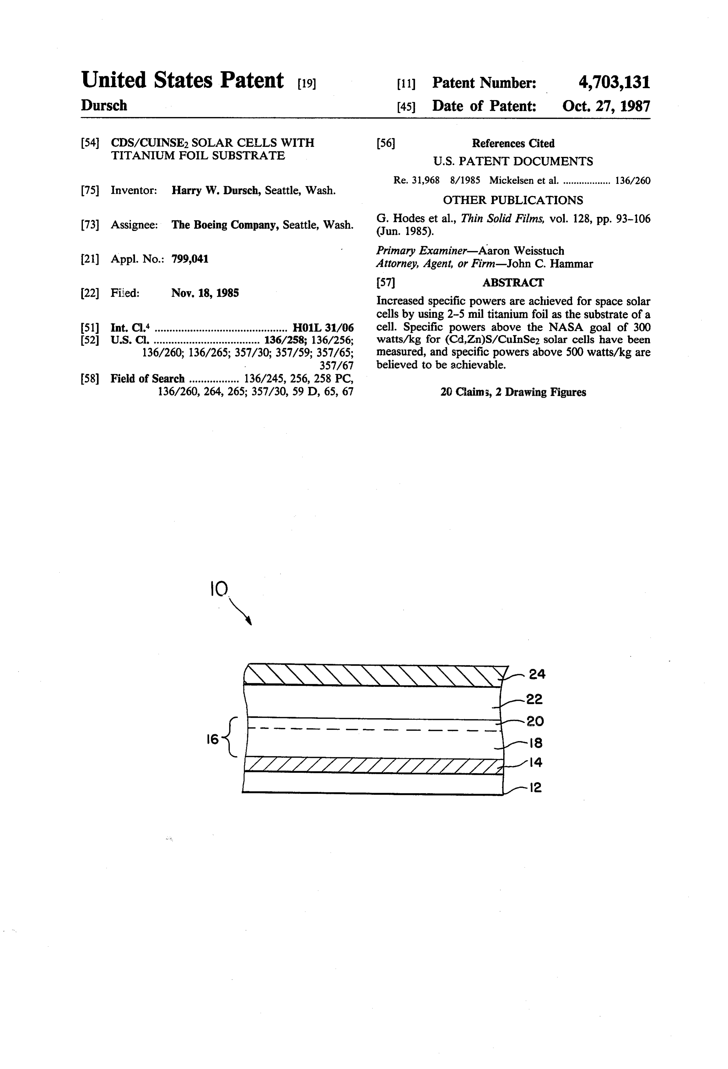
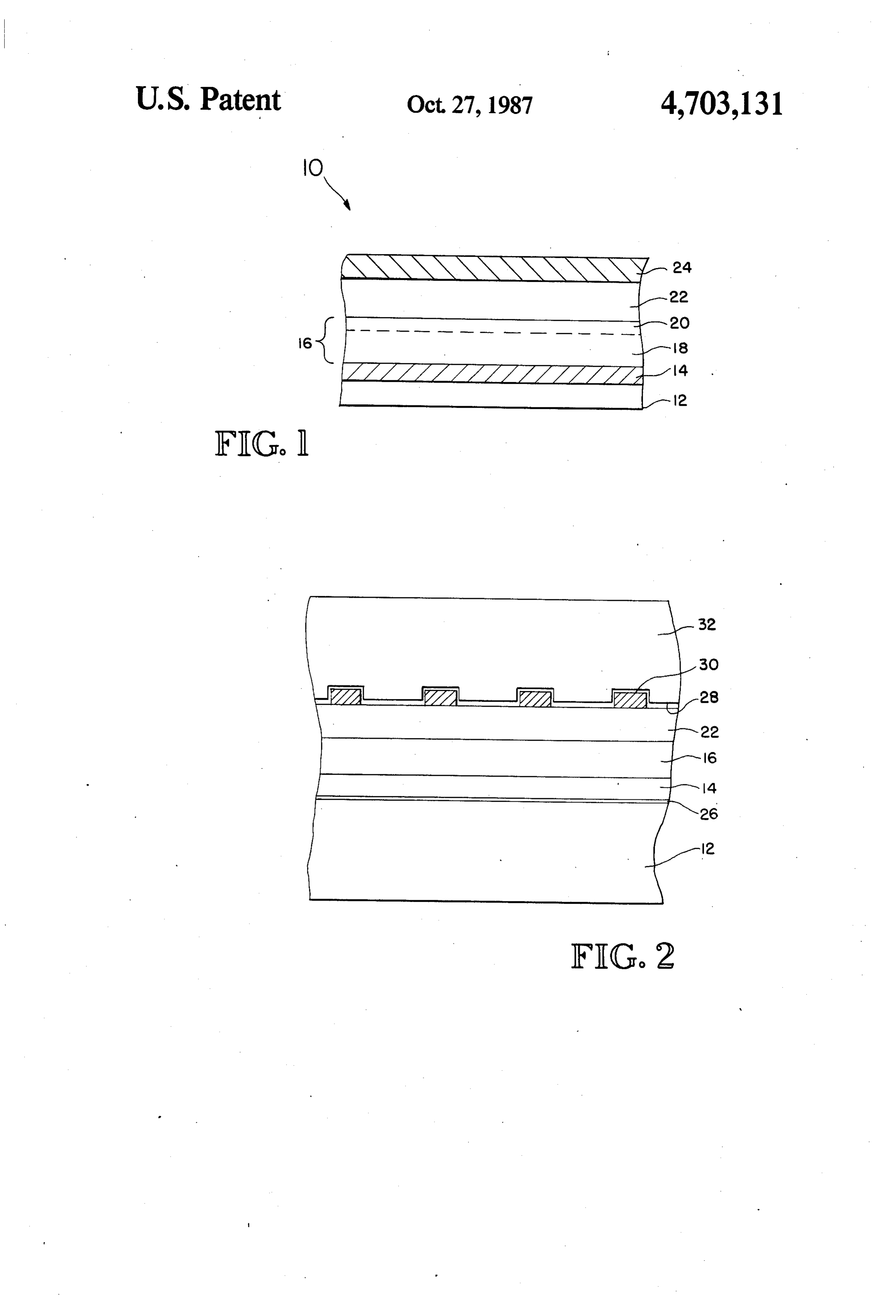
NASA goals for space power arrays call for specific BRIEF DESCRIPTION OF THE DRAWINGS powers for the array in excess of 300 watts/kg so that the mass and drag of the spacecraft power system will FIG. 1 is a schematic cross-section of a solar cell of be reduced and so that the spacecraft, then, can carry 15 the present invention.
larger payloads. Because the hardware of the array only FIG. 2 is a schematic cross-section of another cell. reduces the specific power by adding weight without BEST MODE CONTEMPLATED FOR MAKING increasing the power, the cells of the array must have OR USING THE INVENTION specific powers well in excess of 300 watts/kg if the resulting array will achieve the goal. The solar cell 10 of the present invention preferably is Mickelsen and Chen describe thin film, polycrystal a polycrystalline, thin film, I-III-IV2 chalcopyrite semi line, I-II-VI2 semiconductors suitable for space solar conductor, and, more preferably, a p-CulnSe2/ncells in U.S. Pat. Re. No. 31,968 and U.S. Pat. No. (Cd,Zn)Sheterojunction made according to the method 4,523,051 (both incorporated by reference). Their CuIn of Mickelsen and Chen in U.S. Pat. Re. No. 31,968 and Se2/(Cd, Zn)S cells are deposited on relatively thick U.S. Pat. No. 4,523,051 (both incorporated by refer substrates selected from polycrystalline alumina, glazed 25 ence). Briefly, the Mickelsen and Chen method forms a alumina, enameled steel, metal foils, and similar inert graded, ternary semiconductor free of voids and copper inorganic materials. Typically, the substrate has a thick nodules by simultaneous elemental reactive evapora ness of at least about 25 mils and is preferably either 25 tion. The rates of evaporation of the several elements, mil alumina or 60 mill soda lime glass. Cells of this type the substrate temperature, and the reactor pressure are can have efficiencies on the order of 10% AMO, but the 30 specific power of the cells is dramatically reduced by controlled to achieve high efficiency, polycrystalline thin films.
the mass of the substrate.
As shown in FIG. 1, the cell 10 comprises a 2-5 mil
Presently, silicon solar cells are used for space power titanium applications. I-III-VI2 semiconductor cells, particularly foil. Thismetal foil foil substrate 12, and, preferably, a 2 mil can withstand the high temperatures nec
(Cd,Zn)S/CuInSe2, would provide several advantages: essary for fabricating
the cell (450 C. for 20 min) with (1) The CuInSe2 cell is only 10 microns thick (with out cracking, melting, softening, or distorting. When out substrate) and, therefore, offers the potential of an extremely high specific power. Conventional silicon cooled, the foil retains its desirable mechanical proper cells are 50-100 times thicker. ties. Titanium foil has a coefficient of thermal expansion (2) Radiation testing has shown the CuInSe2 cell to be that essentially matches that of the CunSe2/(Cd,Zn)S 50 times more resistant to 1 MeV protons than silicon cell. This match prevents excessive residual stresses or cells. The CulnSe2 cell also possesses an inherent toler flaking of the cell when cooled to ambient temperature ance to irradiation by 1 MeV electrons up to at least after deposition or during thermal cycling of the cell 2x 10¹⁶ electrons/cm2. At this fluence, typical silicon between about - 175 C. to 100 C., as may be experi cells are degraded by over 50%. Because of the radia 45 enced in space applications. No outgassing occurs from tion hardness of the CunSe2 cell, reduced radiation the substrate during deposition. Finally, and most im shielding is required with CuInSe2 cells which results in portantly, the foil provides the possibility of higher an even higher specific power. By using the equivalent specific powers, since titanium, especially at two mils, is radiation shielding on CuInSe2 cells as on silicon cells, a as light a substrate as heretofore believed possible. The higher end of life efficiency can be achieved for CuIn 50 foil increases the specific power since it reduces the Se2 as well as a higher specific power. volume of material and exhibits a low density (kg/cm). (3) Annealing of the cell, after proton irradiation, at Specific powers above 350 watts/kg for completed cells 200 C. for six minutes restored the CuInSe2 cell to are achievable and possibly as high as 500-1000 within 95% of its initial efficiency. watts/kg when the efficiency is optimized. The major limiting factor against using CulnSe2 cells 55 A thin film base contact 14, preferably of molybde for space applications has been a low specific power for num, is deposited on the substrate 12 by sputtering. the cells primarily caused by the substrate mass. While Then, a graded ternary layer 16 of CulnSe2 is deposited soda lime glass or alumina substrates are satisfactory for by reactive evaporation. Improved semiconductors are terrestrial applications, the cells deposited on the sub formed by controlling the mean free path between strates possess a low specific power. Therefore, a much 60 vapor particles in the reactor by increasing the pressure lighter substrate is required to achieve NASA's goal to produce a homogeneous mixture, as described in U.S. and to meet the demands for modern space power appli Pat. No. 4,432,051. As suggested by Walter Devaney of cations The Boeing Company, the CuInSe2 layer 16 can be
SUMMARY OF THE INVENTION
further improved by controlling the evaporation rates 65 for Cu and Se independently throughout the deposition
The present invention relates to I-III-VI2 semicon and particularly in the initial deposition of CunSe2 onto ductor having a higher specific power than conven the Mo contact 14, in the bulk of the thin film, and in the tional cells and being suitable for use in modern space region near the junction of the film. The substrate tem
Page 4
perature should also be controlled throughout the depo photoactive layers are formed. This interface layer has sition. two regions to make the transition in steps. The first The CuInSe2 layer 16 has two different composition transition region preferably is an n-type ZnSethin film graded regions 18 and 20 sequentially formed with one deposited by low temperature, plasma enhanced CVD region 18 having a first preselected ratio of the elements at temperatures no greater than about 350° C. to avoid in the ternary semiconductor material so as to form a detrimental elemental interdiffusion at the junction. low resistivity semiconductor region and the other re This region is about 0.5-2.0 microns thick, and has de gion 20 having a different preselected ratio of the ele generate doping with copper in the region away from ments so as to form a high resistivity, transient semicon the photoactive junction with CuInSe2. ductor region. The two regions define a transient homo 10 Although plasma enhanced deposition is preferred to junction. Essentially, one region 20 is deficient in cop reduce the deposition temperatures required to grow per near the photoactive junction while the other re the films, it is possible to use other enhancement tech gion 18 is copper-rich to form a p-n type junction. niques, such as OMCVD or laser technologies, to de While CuInSe2 is preferred for the cell 10, other ma posit these films.
terials in the I-III-IV2 chalcopyrite semiconductor fam 15 Atop ily might be used, such as a thin-film A-B-type hetero ited by the n-ZnSe, a second region of p-ZnTe is depos plasma enhanced CVD at low temperatures.
junction where “A” and “B” are selected from the This region is about 0.5-3.0 microns thick, and has de group of semiconductor materials consisting of: generate doping with phosphorus or copper in the re
gion away from the upper photoactive junction where
A and B it contacts the underlying ZnSe surface. i a p-type ternary material and an n-type material; The CunSe2 to ZnSe lattice mismatch is only about iian n-type ternary material and a p-type material; 2.0% and can be eliminated by utilizing CdZnSe. The iii an n-type material and a p-type ternary material; mismatch between ZnSe/ZnTe is only about 0.4%. iv a p-type material and an n-type ternary material 25 Therefore, a graded interface layer of CdZnSe/ZnTe is suitable to interconnect the CunSe2 active layer to an
These other materials, such as AgInS2, AgCiaSe2, or upper layer of CdSe. If other I-III-VI2 chalcopyrites or AgGaTe2, as disclosed in U.S. Pat. Re. No. 31,968, may II-VI heterojunctions are used in the tandem, the inter only have limited application in solar cells. face connector should be selected to achieve this type of A (Cd,Zn)S layer 22 on the CuInSe2 forms a hetero 30 smoothly stepped transition. Furthermore, the interface junction, as explained by Mickelsen and Chen. The connector should be transparent to energy passing resulting cell 10 is a low-cost, polycrystalline trans through the upper photoactive layer.
ducer having an efficiency of at least about 8-10% The ZnSe/ZnTe layer minimizes the propagation of AMO and a specific power above the NASA goal of lattice defects from the lower to the upper junction. 300 watts/kg. Low temperature deposition minimizes dopant redis One or more layers 24 of an antireflection coating can 35 be applied atop the CdS layer 22 to enhance the cell tribution within each region, thereby avoiding undesir able reactions at the film interfaces.
efficiency. SiO, MgF2, and other conventional antire The monolithic cell is completed by depositing n flection coatings can be used. As shown in FIG. 2, the CdSe, a II-VI semiconductor, in a thin film layer of preferred complete cell 10 also includes a grid contact 30 atop the (Cd,Zn)S and a dielectric film 26 of Si3N4 or about 3-5 microns thickness onto the ZnTe region by of another compatible material between the foil and Mo reactive evaporation, and then by depositing a SnO2:F contact. To provide additional radiation resistance and or ZnO ni-type layer by CVD on the CdSe. One or to environmental stability, and protect the cell array more layers of an antireflection coating can be applied during handling, the cells may be coated with about a 2 above the n-type layer to improve cell efficiencies. mil cover layer of FEP-Teflon, another suitable poly 45 EXAMPLE 1 mer, or a glass cover layer.
Cells of this general type are particularly suited for Several 1 cm2 CuInSe2/(Cd,Zn)S cells were depos use in tandem cells. In a mechanically-stacked tandem ited on 5 mill titanium foil using standard cleaning and cell, where the upper cell has a band gap of about deposition techniques. In cell efficiency testing (without 1.4-1.8 eV, and the bottom cell, a band gap of about 1.0 50 an antireflection coating), these cells exhibited an effi eV, the upper cell may be silicon, GaAs, CLEFT ciency of about 7.9% AMO. Stability tests confirmed GaAs, GaAlAs, CLEFT GaAlAs, or a II-VI hetero that the cells were substantially as stable as cells on glass junction, particularly n-CdSe/p-ZnTe, as suggested by or alumina.
Billy Stanbery of The Boeing Company. The lowest EXAMPLE 2 cost with a surprisingly high resistance to radiation 55 damage and with moderately high efficiencies (leading Hypothetical calculations were made regarding the to specific powers in excess of 300 watts/kg for the specific power of a 10% AMO cell using a Si3N4 dielec arrays) are achievable with a CdSe/ZnTe-Culin tric 26 (FIG. 2) between the 2 mill substrate 12 and Se2/(Cd,Zn)S tandem, with the CunSe2/(CdZn)S contact 14, an SiOx antireflection coating 28, an alumi being deposited on titanium foil. 50 num wire grid 30, and a 2 mil FEP-Teflon cover layer The titanium foil substrate can also be used in a mono 32. Cells of this type have a specific power in excess of lithic I-III-VI2/II-VI tandem cell, also as suggested by 400 watts/kg.
Billy Stanbery. There, the substrate has a Mo contact EXAMPLE 3 and a graded CuInSe2 thin film, as in the mechanically stacked cell previously described. The monolithic cell 65 Several 1 cm2 CulnSe2/(Cd,Zn)S cells were depos requires an interface layer so that the lattice mismatch ited on 5 mill titanium foil using a modified Mickel between the CuInSe2 and the upper photoactive layer sen/Chen process where the concentration of copper of the tandem is accommodated, and junctions for the was carefully controlled. Cell efficiencies as high as
Page 5
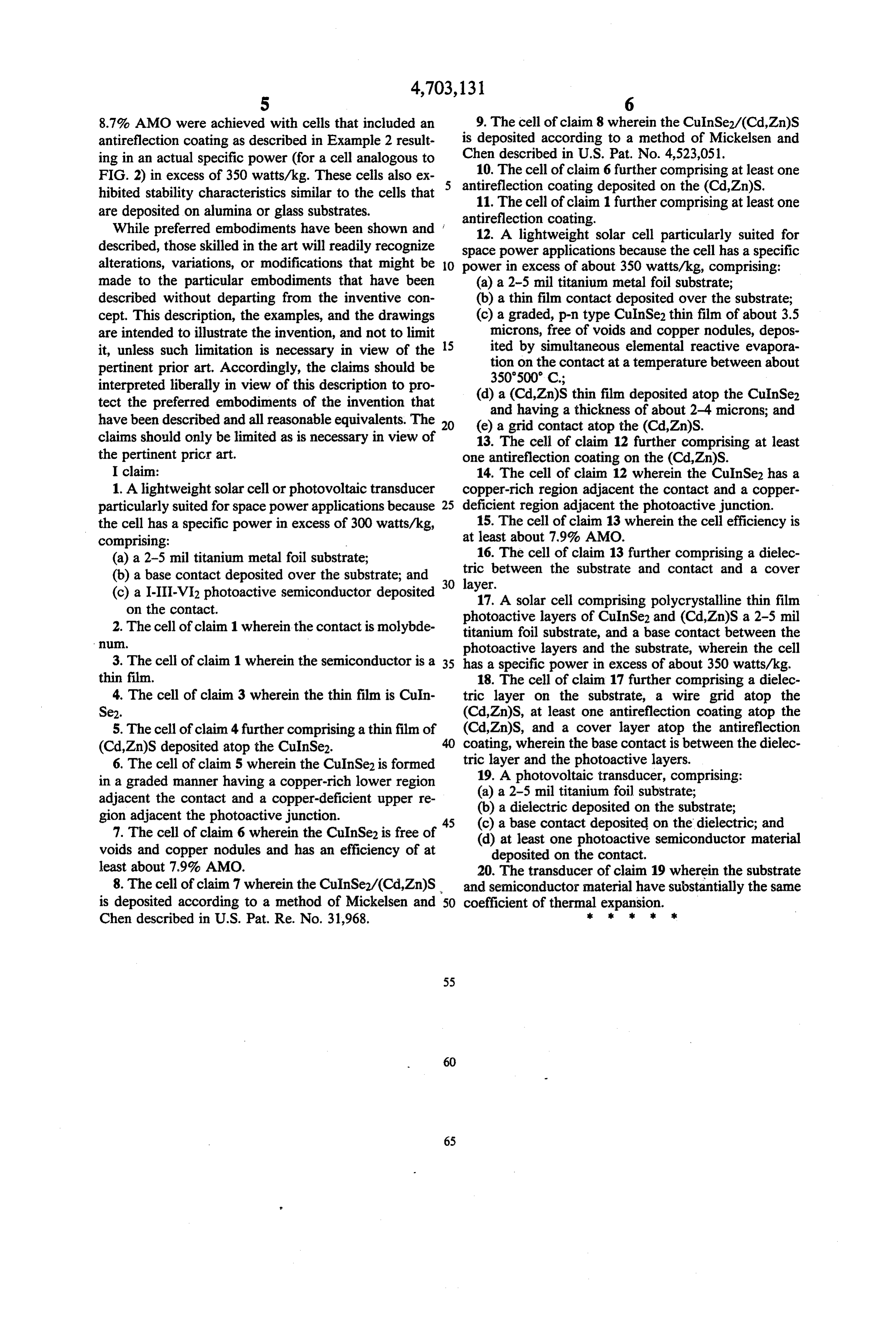
8.7% AMO were achieved with cells that included an 9. The cell of claim 8 wherein the CuInSe2/(Cd,Zn)S antireflection coating as described in Example 2 result is deposited according to a method of Mickelsen and ing in an actual specific power (for a cell analogous to Chen described in U.S. Pat. No. 4,523,051. 10. The cell of claim 6 further comprising at least one
FIG. 2) in excess of 350 watts/kg. These cells also ex antireflection hibited stability characteristics similar to the cells that coating deposited on the (Cd,Zn)S. are deposited on alumina or glass substrates. 11. The cell of claim 1 further comprising at least one antireflection coating.
While preferred embodiments have been shown and 12. A lightweight solar cell particularly suited for described, those skilled in the art will readily recognize space power applications because the cell has a specific alterations, variations, or modifications that might be O power in excess of about 350 watts/kg, comprising: made to the particular embodiments that have been (a) a 2-5 mill titanium metal foil substrate; described without departing from the inventive con (b) a thin film contact deposited over the substrate; cept. This description, the examples, and the drawings (c) a graded, p-n type CuInSe2 thin film of about 3.5 are intended to illustrate the invention, and not to limit microns, free of voids and copper nodules, depos it, unless such limitation is necessary in view of the S ited by simultaneous elemental reactive evapora pertinent prior art. Accordingly, the claims should be tion on the contact at a temperature between about interpreted liberally in view of this description to pro 350°500° C.;
tect the preferred embodiments of the invention that (d) a (CdZn)S thin film deposited atop the CuInSe2 have been described and all reasonable equivalents. The and having a thickness of about 2-4 microns; and claims should only be limited as is necessary in view of (e) a grid contact atop the (Cd,Zn)S.
13. The cell of claim 12 further comprising at least the pertinent pric r art. one antireflection coating on the (Cd,Zn)S. I claim: 14. The cell of claim 12 wherein the CuInSe2 has a 1. A lightweight solar cell or photovoltaic transducer copper-rich region adjacent the contact and a copper particularly suited for space power applications because 25 deficient region adjacent the photoactive junction. the cell has a specific power in excess of 300 watts/kg, 15. The cell of claim 13 wherein the cell efficiency is comprising: m at least about 7.9% AMO.
(a) a 2-5 mill titanium metal foil substrate; 16. The cell of claim 13 further comprising a dielec (b) a base contact deposited over the substrate; and 30 layer.between the substrate and contact and a cover tric (c) a I-III-VI2 photoactive semiconductor deposited 17. A solar cell comprising polycrystalline thin film on the contact.
2. The cell of claim 1 wherein the contact is molybde titanium foil layers photoactive of CuInSe2 and (Cd,Zn)S a 2-5 mil substrate, and a base contact between the photoactive layers and the substrate, wherein the cell 3. The cell of claim 1 wherein the semiconductor is a 35 has a specific power in excess of about 350 watts/kg. thin film. 18. The cell of claim 17 further comprising a dielec 4. The cell of claim 3 wherein the thin film is CuIn tric layer on the substrate, a wire grid atop the Se2. (Cd,Zn)S, at least one antireflection coating atop the 5. The cell of claim 4 further comprising a thin film of (Cd,Zn)S, and a cover layer atop the antireflection (Cd,Zn)S deposited atop the CuInSe2. 40 coating, wherein the base contact is between the dielec 6. The cell of claim 5 wherein the CuInSe2 is formed tric layer and the photoactive layers. in a graded manner having a copper-rich lower region 19. A photovoltaic transducer, comprising: adjacent the contact and a copper-deficient upper re (a) a 2-5 mill titanium foil substrate; gion adjacent the photoactive junction. (b) a dielectric deposited on the substrate; 7. The cell of claim 6 wherein the CuInSe2 is free of 45 (c) a base contact deposited on the dielectric; and voids and copper nodules and has an efficiency of at (d) at least one photoactive semiconductor material deposited on the contact.
least about 7.9% AMO. 20. The transducer of claim 19 wherein the substrate 8. The cell of claim 7 wherein the CuInSe2/(CdZn)S. and semiconductor material have substantially the same is deposited according to a method of Mickelsen and 50 coefficient of thermal expansion.
Chen described in U.S. Pat. Re. No. 31,968.
Provenance
- Collection
- Cited prior art
- Original PDF
- patentimages.storage.googleapis.com →
- Filed
- 1985-11-18
- Pages
- 5
- Method
- pdftotext (the PDF's own text layer) + pdftoppm 300dpi page scans
- Source
- Google Patents bibliographic record
- Granted
- 1987-10-27
- Inventors
- Harry W. Dursch; Boeing Co
- Transcribed from
- patentimages.storage.googleapis.com →