patent · US4695674
Preformed, thin-film front contact current collector grid for photovoltaic cells
22 September 1987
Page 1 — bibliographic record
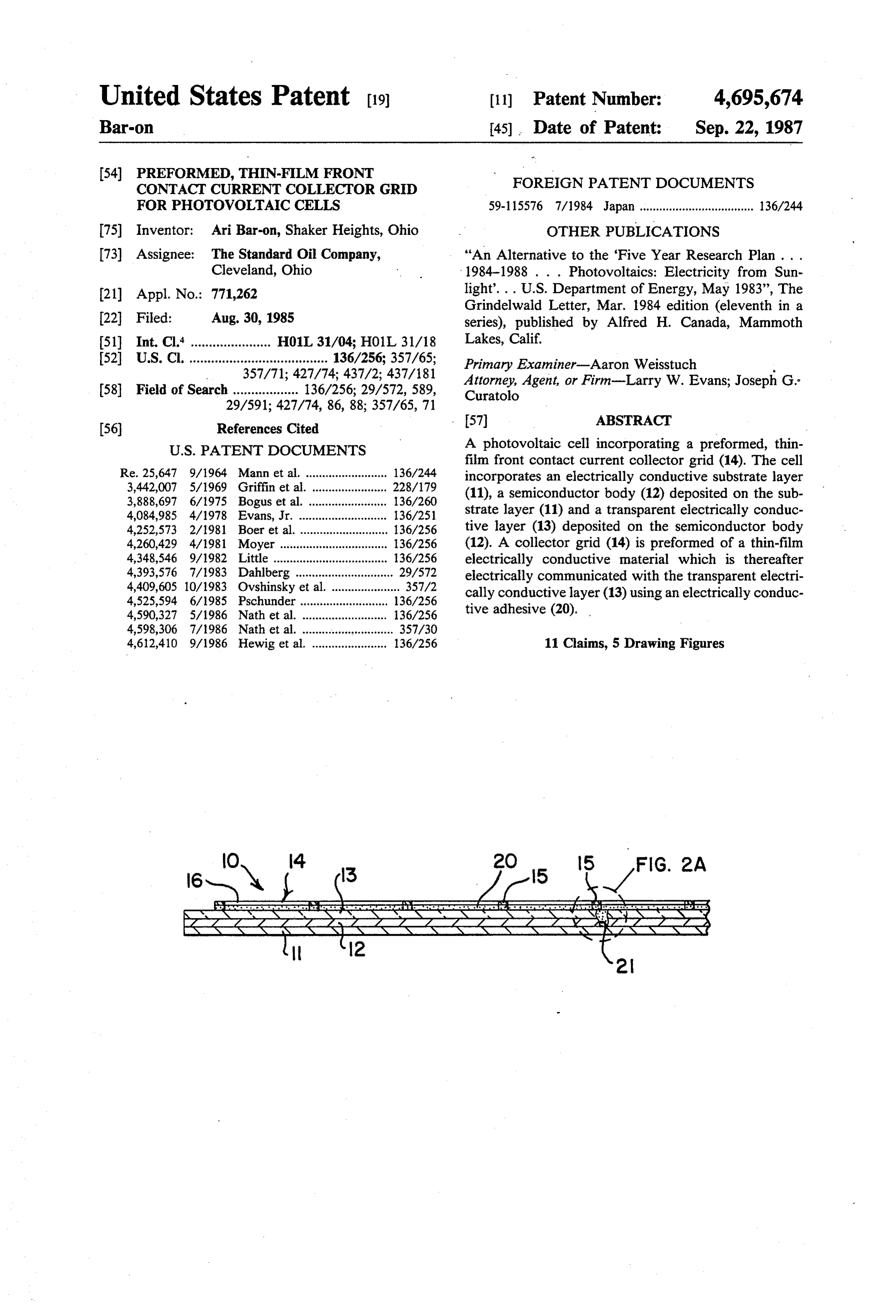
United States Patent (19) (11) Patent Number: 4,695,674 Bar-on 45) Date of Patent: Sep. 22, 1987 54 PREFORMED, THIN-FILM FRONT FOREIGN PATENT DOCUMENTS
CONTACT CURRENT COLLECTOR GRD
FORPHOTOVOLTAC CELLS 59-115576 7/1984 Japan ................................... 36/244 75 Inventor: Ari Bar-on, Shaker Heights, Ohio OTHER PUBLICATIONS (73) Assignee: The Standard Oil Company, “An Alternative to the "Five Year Research Plan . . . Cleveland, Ohio 1984-1988 . . . Photovoltaics: Electricity from Sun 21) Appl. No.: 771,262 light'. ... U.S. Department of Energy, May 1983', The Grindelwald Letter, Mar. 1984 edition (eleventh in a 22 Filed: Aug. 30, 1985 series), published by Alfred H. Canada, Mammoth 51 Int. Cl. ..... - H01L 31/04; HO1L 31/18 Lakes, Calif.
52 U.S. Cl. ...................................... 136/256; 357/65; Primary Examiner-Aaron Weisstuch 8 357/71; 427/74; 437/2; 437/181 Attorney, Agent, or Firm-Larry W. Evans; Joseph G.
58 Field of Search. 136/256; 29/572, 589, Curatolo
(56) References Cited 57 ABSTRACT
film front contact current collector grid (14). The cell
Re. 25,647 9/1964 Mann et al. ......................... 136/244 incorporates an electrically conductive substrate layer 3,442,007 5/1969 Griffin et al. ....................... 228/179 (11), a semiconductor body (12) deposited on the sub 3,888,697 6/1975 Bogus et al. ........................ 136/260 4,084,985 4/1978 Evans, Jr. ........................... 136/251 strate layer (11) and a transparent electrically conduc 4,252,573 2/1981 Boer et al. ........................... 36/256 tive layer (13) deposited on the semiconductor body 4,260,429 4/1981 Moyer ................................. 136/256 (12). A collector grid (14) is preformed of a thin-film 4,348,546 9/1982 Little ................................... 136/256 electrically conductive material which is thereafter 4,393,576 7/1983 Dahlberg .............................. 29/572 electrically communicated with the transparent electri 4,409,605 10/1983 Ovshinsky et al. ..................... 357/2 cally conductive layer (13) using an electrically conduc 4,525,594 6/1985 Pschunder ........................... 136/256 4,590,327 5/1986 Nath et al. .......................... 136/256 tive adhesive (20).
4,598,306 7/1986 Nath et al. ............................ 357/30 4,612,410 9/1986 Hewig et al. ....................... 136/256 11 Claims, 5 Drawing Figures
Page 2
Drawing sheet — no readable text.
Page 3
to the short through the grid and interconnects, thereby
PREFORMED, THIN-FILM FRONT CONTACT rendering a considerable area of the array inoperable. CURRENT COLLECTOR GRD FOR Thus, the time, money, and effort expended in fabricat PHOTOVOLTAC CELLS ing the photovoltaic cell, including deposition of the
TECHNICAL FIELD
grid, are lost. These losses result in an increased overall cost in the production of workable photovoltaic cells
The present invention relates generally to photovol and arrays.
taic cells. More particularly, the present invention re Efforts have been made to form front contact current lates to front contact current collector grids for photo 10 collector grids by methods other than in situ fabrica voltaic cells. Specifically, the present invention pertains tion. Exemplary of these efforts is U.S. Pat. No. to a front contact current collector grid preformed from 4,348,546 to Little wherein a mesh of fine wires is en a thin, electrically conductive film. capsulated between a transparent cover plate and the BACKGROUND ART front surface of the semiconductor strata during fabrica tion of the solar cell. Use of fine wire as a front contact
Developments made in harnessing solar energy have 15 current collector for solar cells is also discussed in "An resulted in three primary types of photovoltaic Alternative to the "Five Year Research Plan . . . devices-namely, crystalline solar cells, semi-crystal 1984-1988 . . . Photovoltaics: Electricity from Sun line solar cells, and amorphous solar cells. Each of these light'. . . U.S. Department of Energy, May 1983', the solar cell types produces electricity as a result of what Grindewald Letter, March 1984 edition (Eleventh in a
is commonly known in the solar cell field as the photo series), published voltaic effect. This is an inherent feature of a semicon by Alfred H. Canada, Mammoth ductor region in the photovoltaic device. Lakes, Calif.
In the fabrication of photovoltaic cells, as for exam in Despite the the substantial work and research conducted production of photovoltaic cells and arrays, no ple amorphous solar cells, it is necessary to provide practical solutions have been developed to alleviate the means for collecting the current produced from the cell. 25 aforesaid
On the back of the cell, the surface not exposed to solar problems in fabricating the front contact cur radiation, an electrically conductive substrate layer, rent collector grids.
such as stainless steel, is employed to which an electri DISCLOSURE OF THE INVENTION cal connection can be made. On the front surface of the cell, a transparent conductive oxide (TCO) layer and an 30 Therefore, an object of the present invention is a electrically conductive grid generally are employed photovoltaic cell having an electrically conductive which enable electrical current to be collected from the substrate layer, a semiconductor body deposited on the semiconductor region of the cell without unduly ob substrate layer and a transparent electrically conductive scuring the incidence of solar radiation to the interior of layer deposited on the semiconductor body. A pre the cell. For a general discussion of the structure and 35 formed thin-film electrically conductive grid is em function of amorphous silicon cells and the means of ployed having a preselected physical configuration. collecting current therefrom, reference may be made to The preformed grid is electrically communicated with U.S. Pat. No. 4,409,605 to Ovshinsky et al. the transparent electrically conductive layer of the pho Several techniques are presently employed for fabri tovoltaic cell.
cating the front contact grid of photovoltaic cells. Another object of the present invention is a pre These techniques involve the fabrication of the grid formed thin-film front contact current collector grid for directly onto the transparent conductive layer of the a photovoltaic cell. The grid includes a plurality of cell. Exemplary of this in situ fabrication of the grids are fingers oriented in a predetermined configuration and a screen printing with conductive ink, and electroform collector bus integrally associated with the fingers. The plating using a mask to form a preselected pattern. 45
These techniques, in addition to being time consuming collector bus and the fingers collectively define the from a production aspect, present inherent problems in current collecting structure of the grid. The collector the fabrication of photovoltaic cells. Particularly, the bus and the fingers further define a contact surface for grids thus formed are not readily electrically intercon electrically communicating with the photovoltaic cell. nected when multiple cells are assembled into a photo 50 of disposing object
A further of the present invention is a method voltaic array. The small area of the grids, coupled with photovoltaicacell front contact current collector grid on a having a transparent conductive layer.
the material used, for example silver ink for screen The method includes printing, precludes favorable soldering or welding of conductive material intothea predetermined steps of forming a thin-film configuration the interconnectors to the grid. of a grid, and locating the grid relative to the transpar In addition to the foregoing problem, in situ fabrica 55 ent conductive layer of the photovoltaic cell. The grid tion of grids is more likely to cause shorting of the photovoltaic cell. This occurs because as the semicon is communicated electrically with the transparent con ductor body and transparent conductive layer are de ductive layer.
posited on the substrate, during fabrication of the cell, Yet a further object of the present invention is a pro minute holes, voids or other defects are inevitably cess for fabricating a photovoltaic cell. The process formed therein. Though generally not a problem in the includes depositing a semiconductor body on an electri operation of the cell, such holes, voids or defects may cally conductive substrate layer. A transparent electri be filled with the conductive material of the grid at the cally conductive layer is deposited on the semiconduc time the latter is being fabricated on the cell. When this tor body. A thin-film conductive material is formed into happens, the cell is essentially irrevocably shorted, the 65 a predetermined configuration of a grid and located transparent conductive layer being shorted to the con relative to the transparent conductive layer. The grid is ductive substrate. Moreover, current generated by communicated electrically with the transparent con other cells in the photovoltaic array is likewise drawn ductive layer.
Page 4
Exemplary embodiments of preformed, thin-film Grid 14 is preferably made of thin-film material, as electrically conductive grids incorporating the concept depicted in FIG. 3. Instead, depending upon the specific of the present invention are shown by way of example material employed, the thickness of the film from which in the accompanying drawings without attempting to grid 14 is made is approximately 1 to 3 mils (0.025 to show all the various forms and modifications in which 5 0.076 mm). This thin-film material is pre-cut to form a the invention might be embodied, the invention being grid 14 of a desired configuration, as by a die cutting measured by the appended claims and not by the details process for example, to meet the requirements of the of the specification. specific photovoltaic cells. Generally, grid 14 has a
BRIEF DESCRIPTION OF THE DRAWINGS
plurality of narrow fingers 15 integrally associated
O with, and depending from, a common collector bus 16.
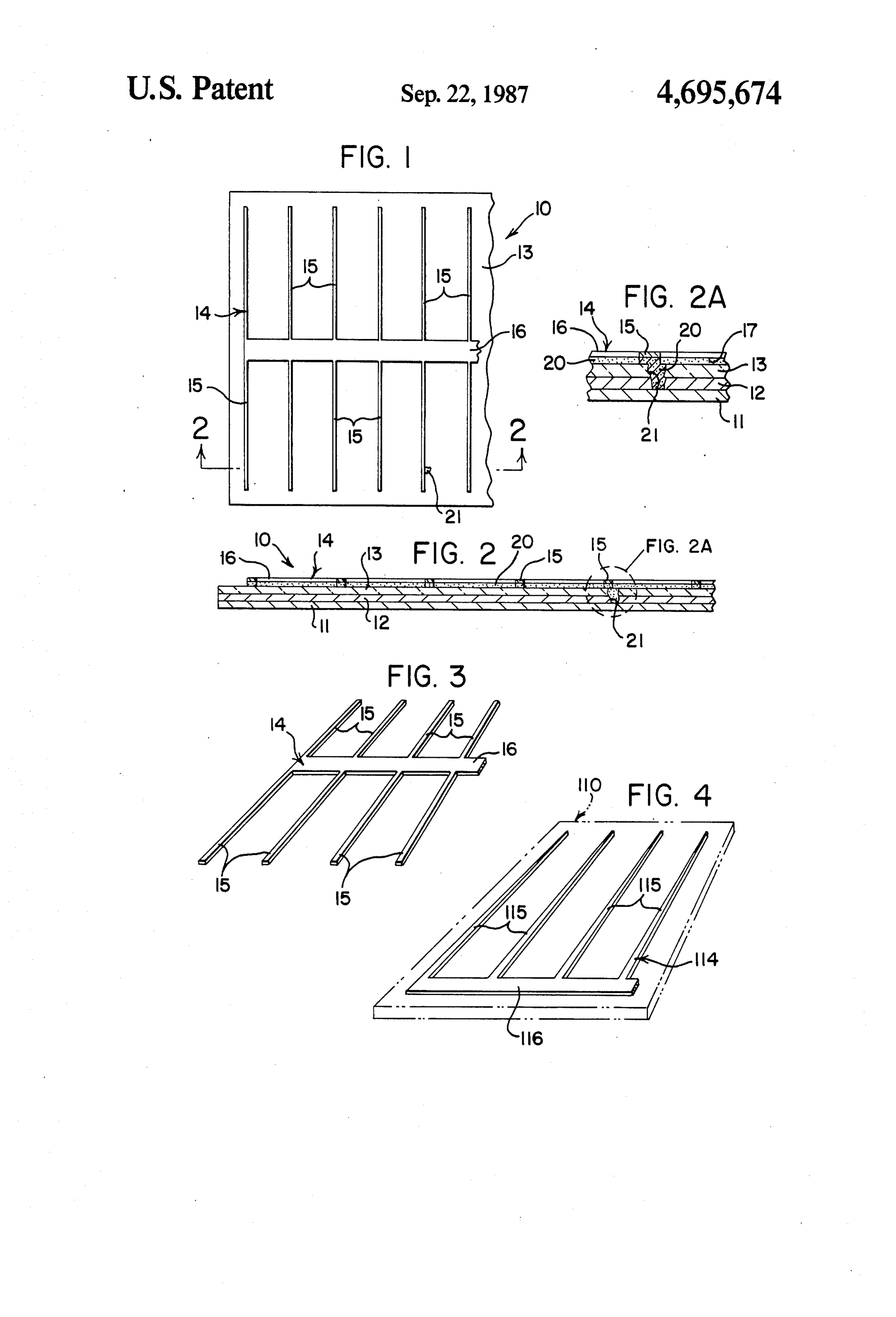
FIG. is a fragmentary plan view of a photovoltaic The fingers 15 and collector bus 16 collectively define cell embodying the concept of the present invention; the current collector structure of grid 14, which struc FIG. 2 is an enlarged fragmentary cross-section of a ture presents a contact surface 17, shown in FIG. 2A, to photovoltaic cell taken substantially along line 2-2 of 15 facilitate electrical communication with transparent FIG. 1; conductive layer 13.
FIG. 2A is an enlarged cross-sectional inset of the Inasmuch as grid 14 is made from opaque material, region indicated in FIG. 2; the surface area of grid 14 must be kept to a minimum so FIG. 3 is a fragmentary perspective view of a front as to reduce losses caused by shadowing of the cell. For contact current collector grid embodying the concept 20 the configuration of grid 14 depicted in FIG. 3, each of the present invention; and, finger 15 preferably has a plan width of approximately FIG. 4 is a fragmentary perspective view of an alter 10 mils (0.25 mm), and is spaced approximately 0.2 inch native embodiment of a front contact current collector (5.1 mm) from adjacent fingers. Similarly, collector bus grid according to the present invention. 16 preferably has a plan width of approximately 0.1 inch EXEMPLARY EMBODIMENT FOR CARRYING 25 course, (2.5 mm) or less. Other dimensional parameters, of
OUT THE INVENTION
are contemplated. Determinative factors defin ing the physical parameters of grid 14 include the junc
A photovoltaic cell according to the concept of the tion type of the cell-single junction, tanden junction, present invention is indicated generally by the numeral etc.-the voltage potential of the cell, and the ideal 10 in FIG. 1 of the accomanying drawings. The photo resistance of the grid and the transparent conductive voltaic cell 10 shown is of the general configuration of layer.
an amorphous silicon solar cell although the concept of With grid 14 being fabricated independently of the the present invention is equally applicable to all types of cell 10, operative association therewith is achieved solar cells, including crystalline solar cells, polycrystal through the use of a conductive adhesive 20. Specifi line solar cells, and amorphous solar cells. As depicted 35 cally, conductive adhesive 20 is preferably a hot-melt in FIG. 2, the photovoltaic cell 10 includes an electri type adhesive although other types of adhesive may be cally conductive continuous substrate layer 11, a semi employed. Likewise, conductive adhesive 20 preferably conductor body 12 deposited on the substrate layer 11, possesses an electrical impedance, to the extent of being and a transparent electrically conductive layer 13 de slightly resistive, for purposes as will be appreciated posited on the semiconductor body 12. e 40 hereinbelow. Indeed, conductive adhesive 20 having a Elaborating on these elements slightly, the substrate bulk resistivity of approximately 2 ohms-cm has been layer 11 preferably is a flexible metallic member, such as found to provide acceptable performance for a cell stainless steel. The semiconductor body 12 preferably having a voltage of approximate 1.3 volts, although a includes an N-type layer, an intrinsic (I-type) layer, and broader range of from about 0.5 to 5 ohms-cm is be a P-type layer-collectively referred to as a P-I-N type 45 lieved to be operable for other voltages which photo semiconductor-as normally found in solar cells of the voltaic cells are known to operate. At least one suitable amorphous silicon type. The transparent electrically conductive adhesive is a carbon loaded, polyimide, conductive layer 13 is preferably a thin layer of a trans hot-melt adhesive.
parent conductive oxide, such as indium tin oxide Conductive adhesive 20 is disposed between grid 14 (ITO). It should be appreciated that FIG. 2 is not pre 50 and transparent conductive layer 13. Conductive adhe pared to scale but rather is substantially disproportioned sive 20 is applied to contact surface 17 of grid 14 at a to permit a more detailed representation of the individ thickness of approximately 2 mls (0.05mm). While con ual elements. As a reference, it should be appreciated ductive adhesive 20 can be applied to grid 14 after it has that the semiconductor body 12 is typically less than been formed, conductive adhesive 20 likewise can be one micron thick; and the substrate layer 11 is generally 55 applied to the thinfilm material prior to the grid 14 200 to 300 microns thick. being formed therefrom. Thereafter, grid 14 is located Although transparent layer 13 is, itself, electrically on transparent conductive layer 13 and the adhesion conductive, it may be desirable to employ electrically therebetween is effected at the temperature and com conductive grids 14 to collect efficiently the electrical pressive pressure required for the specific adhesive 20 energy generated over a large area cell, that is, a cell 60 to set, as depicted in FIG. 2. having an active surface area greater than approxi It should be appreciated that with grid 14thus affixed mately 2 cm2. The grids 14 are preferably formed of a to transparent conductive layer 13 with adhesive 20, highly conductive material, such as a conductive metal good electrical communication exists therebetween. or alloy foil-such as, aluminum, copper, silver, gold, Electrical current generated by the photovoltaic cell 10 brass, etc. Although the exact configuration of grid 14 65 is, therefore, collected from transparent conductive may vary to meet the parameters of a specific applica layer 13 by grid 14 for removal therefrom by suitable tion, several features are generally common to each as interconnections as are commonly employed in photo contemplated in the present invention. voltaic arrays and modules. These interconnections
Page 5
would preferably be made to the collector bus 16 of the alternative grid 114 depicted in FIG. 4. Again, grid 114 grid 14. is fabricated of highly conductive thin-film material, It should further be appreciated that when grid 14 is such as a conductive metal foil as discussed above with formed of a conductive metal or alloy foil, as for exam respect to grid 14. This thin-film material is pre-cut to ple aluminum or nickel foil, interconnections therewith form grid 114.
can more readily be effected in a variety of manners. Grid 114 differs primarily from grid 14 in its configu These metals lend themselves more favorably to being ration. Specifically, the fingers 115 are triangular in soldered or ultrasonically welded than does silver ink. shape with the plan width thereof continually decreas Accordingly, electrical interconnection with grid 14 ing toward the tip thereof. Fingers 115 are integrally can be effected using these techinques. Similarly, inter O associated with, and depend in one direction from, col connection can be effected using a conductive adhesive, lector bus 116.
instead of soldering or welding, when the situation The configuration of grid 114 provides several signif. allows, as would be appreciated by one skilled in the art. icant advantages. Collector bus 116 is capable of being The electrical resistance characteristics of the adhe located proximate to an edge of a photovoltaic cell sive 20 is appreciated when the grid 14 happens to be 15 thereby permitting interconnection to be made without located over a minute hole or void 21, or other defect, shadowing the photovoltaic cell. Furthermore, the ta in transparent conductive layer 13 and semiconductor pered configuration offingers 115 permits uniform cur body 12, as depicted in FIG. 2A. Upon installation of rent density to exist throughout fingers 115. As the grid 14, adhesive 20 will tend to flow into and fill hole current flows toward collector bus 116 the accumula 21. Although an electrically conductive path may now tion of current from the cell will necessitate a larger exist between grid 14 and substrate layer 11, the electri conductor path than is required at the most distal end of cal resistance of adhesive 20 will be substantially greater finger 115. Accordingly, the tapered configuration of then that of grid 14. Therefore, current absorbed by fingers 115 provides ample current carrying capacity grid 14 from the remainder of the photovoltaic cell 10 throughout their length while providing minimal sur will follow along the path of least resistance, i.e., grid 25 face area so as to reduce losses due to shadowing of the finger 15 and collector bus 16, rather than shorting with cell.
substrate layer 11. Similarly, current from other cells in It should be appreciated that grid 114 is incorporated an array will not flow to the affected cell and short. It into a photovoltaic cell in the same manner as grid 14. should be appreciated that grid 14 and adhesive 20 Namely, grid 114, being preformed from thin-film mate enable the photovoltaic cell 10, and an array into which 30 rial, is affixed to the transparent conductive layer of a they are incorporated, to remain operable under condi cell by employing a conductive adhesive, as discussed tions which would otherwise have resulted in a dead above. This embodiment will provide the same desir short under prior art fabrication practices, able characteristics and advantages as are attributable to With the structure of grid 14 thus described, a the embodiment incorporating grid 14.
method of incorporating the same into a photovoltaic 35 It should also be appreciated, therefore, that the fore cell 10 having a transparent conductive layer 13 can be going advantages and characteristics are likewise asso appreciated. Specifically, a thin-film conductive mate ciated with grids of other configurations. Indeed, the rial, such as an aluminum foil, is formed into a predeter configuration of a grid will depend primarily on the mined configuration of a grid 14. This is preferably specific photovoltaic cell into which it will be incorpo accomplished with a die cutting process wherein the rated. The concept of employing a grid preformed of a configuration of grid 14 is cut from the thin-film con thin-film conductive material which is thereafter se ductive material. cured to the cell using a conductive adhesive is equally Contact surface 17 of grid 14 is coated with a layer of applicable to other grid configurations. As such, the conductive adhesive 20 and, preferably being a hot-melt foregoing invention should be recognized as constitut type adhesive, is permitted to partially cure. Thereafter, 45 ing a novel and advantageous contribution to the art of grid 14 is located on transparent conductive layer 13 of fabricating photovoltaic cells.
the photovoltaic cell 10 in a predetermined position. I claim:
Suitable pressure and temperature are applied to com 1. A photovoltaic cell comprising: plete the curing process of adhesive 20 and thereby an electrically conductive substrate layer; securely bond grid 14 to transparent conductive layer 50 a semiconductor body deposited on said substrate 13. The cell 10 is then tested by exposure to a radiant layer;
light source to assure correct operation of the cell 10 a transparent electrically conductive layer deposited and particularly the collection of electrical current by on said semiconductor body; s grid 14. preformed thin-film electrically conductive grid It should be appreciated that the foregoing method of 55 means for collecting electrical current from said fabrication can be achieved as a piecemeal operation. cell, said grid means having a predetermined physi However, it should also be recognized that the afore cal configuration; and said method can be effected in a continuous operation. an electrically conductive adhesive on said grid Indeed, continuous grids 14 can be cut from continuous means to physically and electrically connect said strips of thin-film conductive material and serially grid means to said transparent electrically conduc bonded to continuous photovoltaic cell strips. Such an tive layer, said adhesive having a bulk resistive of operation would greatly expedite the fabrication and from about 0.5 ohms-cm to about 5 ohms-cm. production of photovoltaic cells and ultimately reduce 2. The photovoltaic cell according to claim 1 wherein the overall cost thereof. said adhesive possesses a bulk resistivity of approxi The foregoing advantages and characteristics of a 65 mately 2 ohms-cm.
photovoltaic cell 10 of the foregoing embodiment are 3. The photovoltaic cell according to claim 2, likewise associated with a photovoltaic cell 110 incor wherein said grid means comprises a plurality of finger porating other grid configurations as, for example, the means integrally associated with a collector bus means.
Page 6
4. The photovoltaic cell according to claim 3, 5, wherein said adhesive possesses a bulk resistivity of wherein said grid means is a metal foil. approximately 2 ohms-cm.
5. A method of disposing a front contact current 9. A process for fabricating a photovoltaic cell com collector grid on a photovoltaic cell having a transpar 5 prising:
depositing a semiconductor body on an electrically ent conductive layer comprising the steps of: conductive substrate layer; forming a thin-film conductive material into a prede depositing a transparent electrically conductive layer termined configuration of a grid; on said semiconductor body; coating one surface of said grid with an electrically forming a thin-film conductive material into a prede conductive adhesive having a bulk resistivity from 10 termined configuration of a grid; about 0.5 ohms-cm to about 5 ohms-cm; coating one surface of said grid with an electrically locating said grid relative to the transparent conduc conductive adhesive having a bulk resistivity from tive layer of the photovoltaic cell; and about 0.5 ohms-cm to about 5 ohms-cm; bonding said grid to the transparent conductive layer locating said grid relative to said transparent conduc with said electrically conductive adhesive. 15 tive layer; and 6. The method of disposing a front contact current bonding said grid to said transparent conductive layer collector grid on a photovoltaic cell according to claim with said electrically conductive adhesive. 10. The process for fabricating a photovoltaic cell 5, wherein said step of forming is a die cutting process. according 7. The method of disposing a front contact current 20 finger means to claim 9, wherein said grid has a plurality of collector grid on a photovoltaic cell according to claim integrally associated with a collector bus healS.
5, wherein said electrically conductive adhesive is ap i1. The process for fabricating a photovoltaic cell plied to said grid prior to locating said grid on the trans according to claim 10, wherein said electrically conduc parent electrically conductive layer of the photovoltaic tive adhesive impedes flow of electrical current from cell. 25 said grid to defects in the photovoltaic cell when said 8. The method of disposing a front contact current grid is bonded thereto.
collector grid on a photovoltaic cell according to claim sk ski i k sk
Provenance
- Collection
- Cited prior art
- Original PDF
- patentimages.storage.googleapis.com →
- Filed
- 1985-08-30
- Pages
- 6
- Method
- pdftotext (the PDF's own text layer) + pdftoppm 300dpi page scans
- Source
- Google Patents bibliographic record
- Granted
- 1987-09-22
- Inventors
- Ari Bar-on; Standard Oil Co
- Transcribed from
- patentimages.storage.googleapis.com →