patent · US4631474
High or low-side state relay with current limiting and operational testing
23 December 1986
Page 1 — bibliographic record
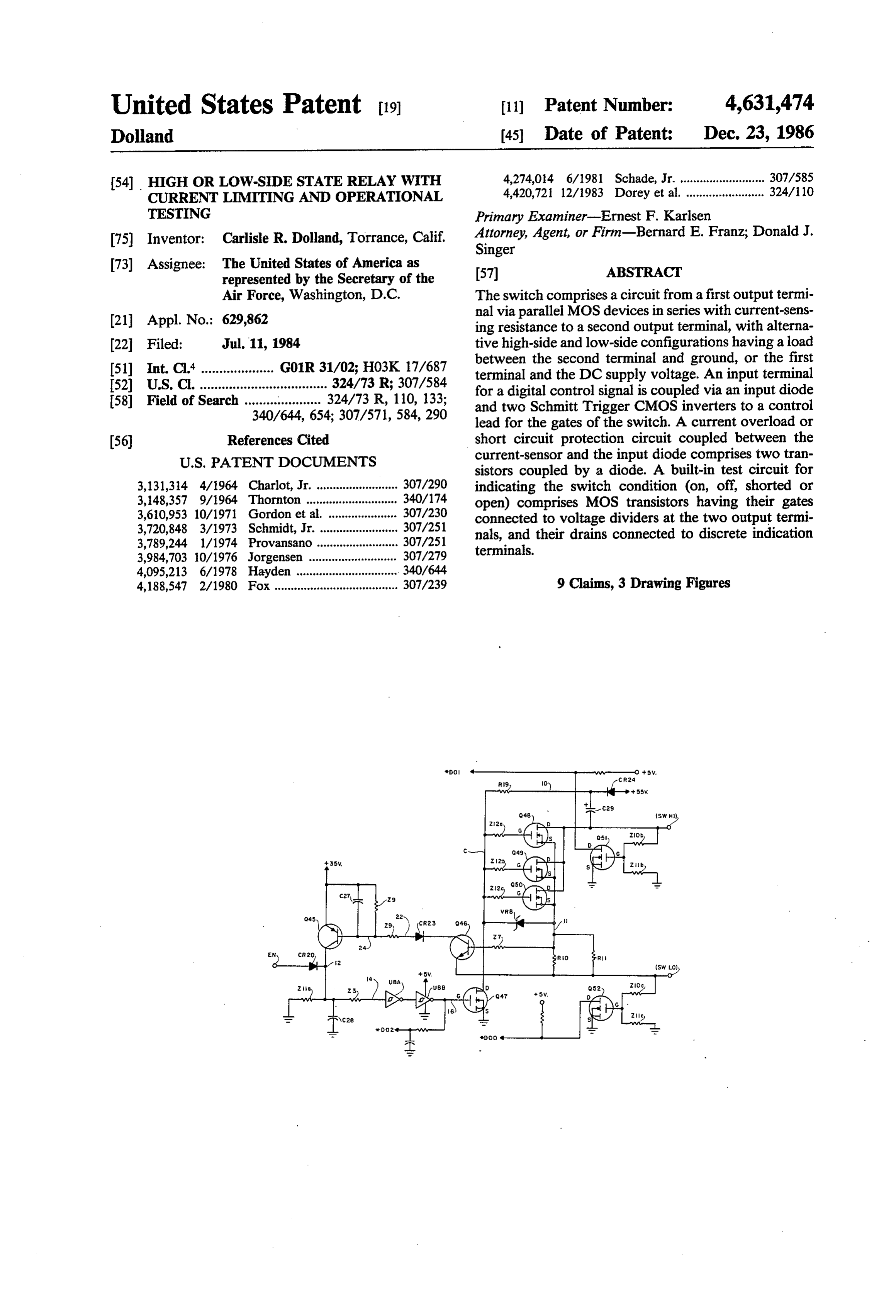
United States Patent (19) 11 Patent Number: 4,631,474 Dolland (45) Date of Patent: Dec. 23, 1986 54) HIGH OR LOW-SIDE STATE RELAY WITH 4,274,014 6/1981 Schade, Jr... esa a 307/585
CURRENT LIMITING AND OPERATIONAL 4,420,721 12/1983 Dorey et al. a are Po w w K a a so 324/10
TESTING Primary Examiner-Ernest F. Karlsen (75) Inventor: Carlisle R. Dolland, Torrance, Calif. Attorney, Agent, or Firm-Bernard E. Franz; Donald J. Singer 73) Assignee: The United States of America as 57 ABSTRACT represented by the Secretary of the
Air Force, Washington, D.C. The switch comprises a circuit from a first output termi 21 Appl. No.: 629,862 nal via parallel MOS devices in series with current-sens ing resistance to a second output terminal, with alterna 22 Filed: Jul.11, 1984 tive high-side and low-side configurations having a load between the second terminal and ground, or the first (51) Int. Cl.' .................... G01R 31/02; H03K 17/687 terminal and the DC supply voltage. An input terminal (52) o do 8 d. 324/73 R; 307/584 for a digital control signal is coupled via an input diode (58) Field of Search ..................... 324/73 R, 110, 133; and two Schmitt Trigger CMOS inverters to a control 340/644, 654; 307/571, 584, 290 lead for the gates of the switch. A current overload or (56) References Cited short circuit protection circuit coupled between the
sistors coupled by a diode. A built-in test circuit for 3,131,314 4/1964 Charlot, Jr. ......................... 307/290 indicating the switch condition (on, off, shorted or 3,148,357 9/1964 Thornton .... , 340/174 open) comprises MOS transistors having their gates 3,610,953 10/1971 Gordon et al. ..................... 307/230 connected to voltage dividers at the two output termi 3,720,848 3/1973 Schmidt, Jr. ........................ 307/251 nals, and their drains connected to discrete indication 3,789,244 1/1974 Provansano ......................... 307/251 terminals.
3,984,703 10/1976 Jorgensen ........................... 307/279 4,095,213 6/1978 Hayden ............................... 340/644 4,188,547 2/1980 Fox ...................................... 307/239 9 Claims, 3 Drawing Figures
Page 2
St -- n N n
Ud co
e ca
C s all g all a C
o o n a CN Q N O n N O
Page 3
Drawing sheet — no readable text.
Page 4
built-in test indications during a specified transient
HIGH OR LOW-SIDE STATE RELAY WITH while short circuit protection remains active. CURRENT LIMITING AND OPERATIONAL The switch according to the invention overcomes TESTING shortcomings of prior switches.
1. It is capable of being operated as either a high-side
RIGHTS OF THE GOVERNMENT switch or a low-side switch.
2. It is short-circuit protected.
The invention described herein may be manufactured 3. It will remain on during the specified transient and and used by or for the Government of the United States will not give a short-circuit indication during this for all governmental purposes without the payment of transient.
any royalty. 4. It's dissipation under a short-circuit condition is sub BACKGROUND OF THE INVENTION stantially less than it is when operating with a nomi nal load.
The present invention relates generally to DC a solid 5. This innovation permits the fabrication of a general state switch which can be operated as a high-side switch 5 purpose switch board for use in military computers which applies voltage to a load, or as a low-side switch (The use of power MOS devices as switch elements which provides a closure to ground for a load, with permits the solid state switch to be expandable to any built-in current limiting and test features relating to the current level without the use of any heatsink compo state of operation. nents).
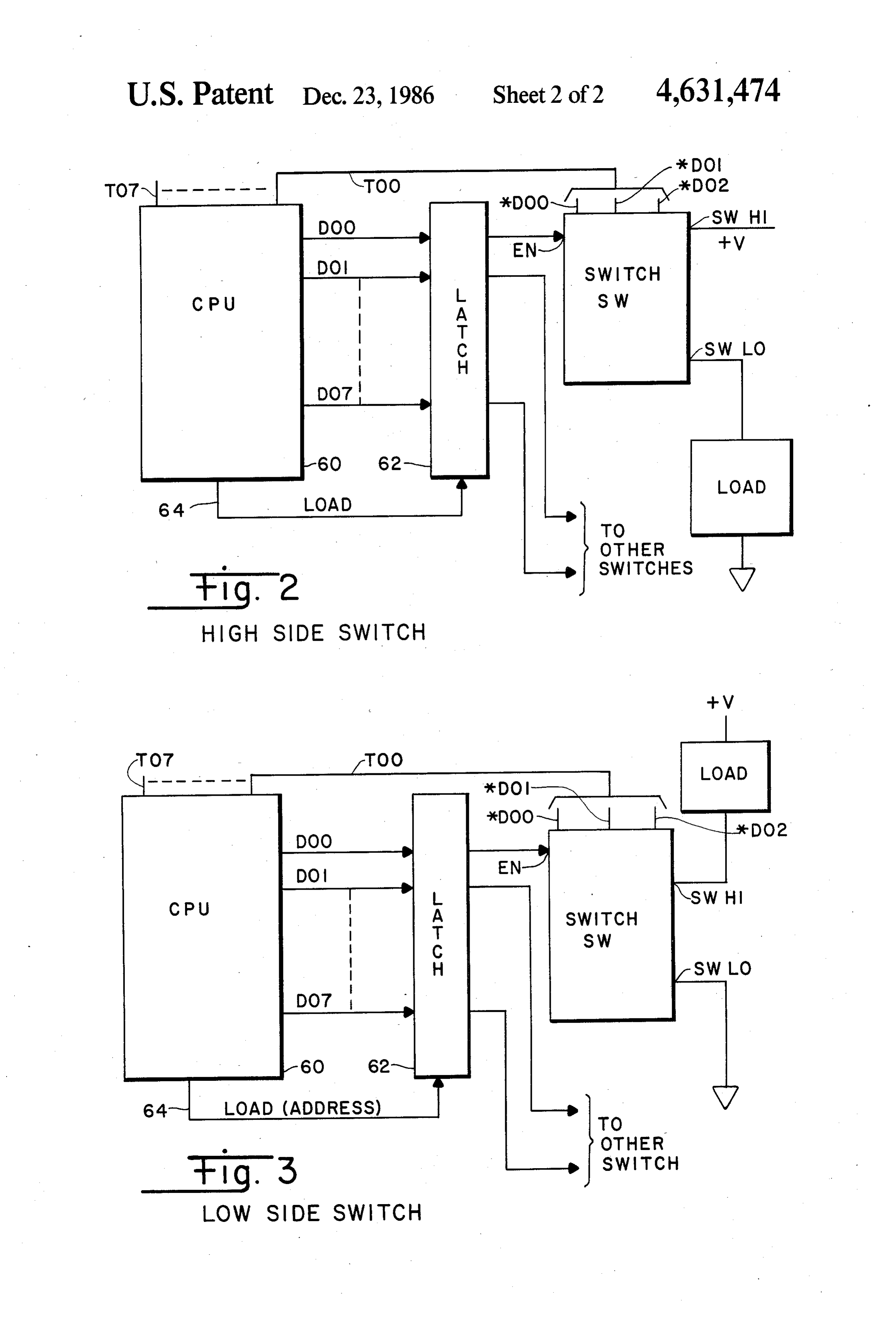
Solid state switches for connecting a direct-current 20 BRIEF DESCRIPTION OF THE DRAWING supply to a load are well known, as shown for example by U.S. Pat. No. 3,148,357 to Thornton and No. FIG. 1 is a schematic diagram of a solid state switch 3,610,953 to Gordon Schade, Jr., U.S. Pat. No. according to the invention; and 4,274,014 shows a solid state switch in the form of a FIGS. 2 and 3 are block diagrams showing the use of complementary symmetry inverter which include cur 25 the switch for high-side and low-side operation respec rent limiting. In the patent current limiting is obtained tively.
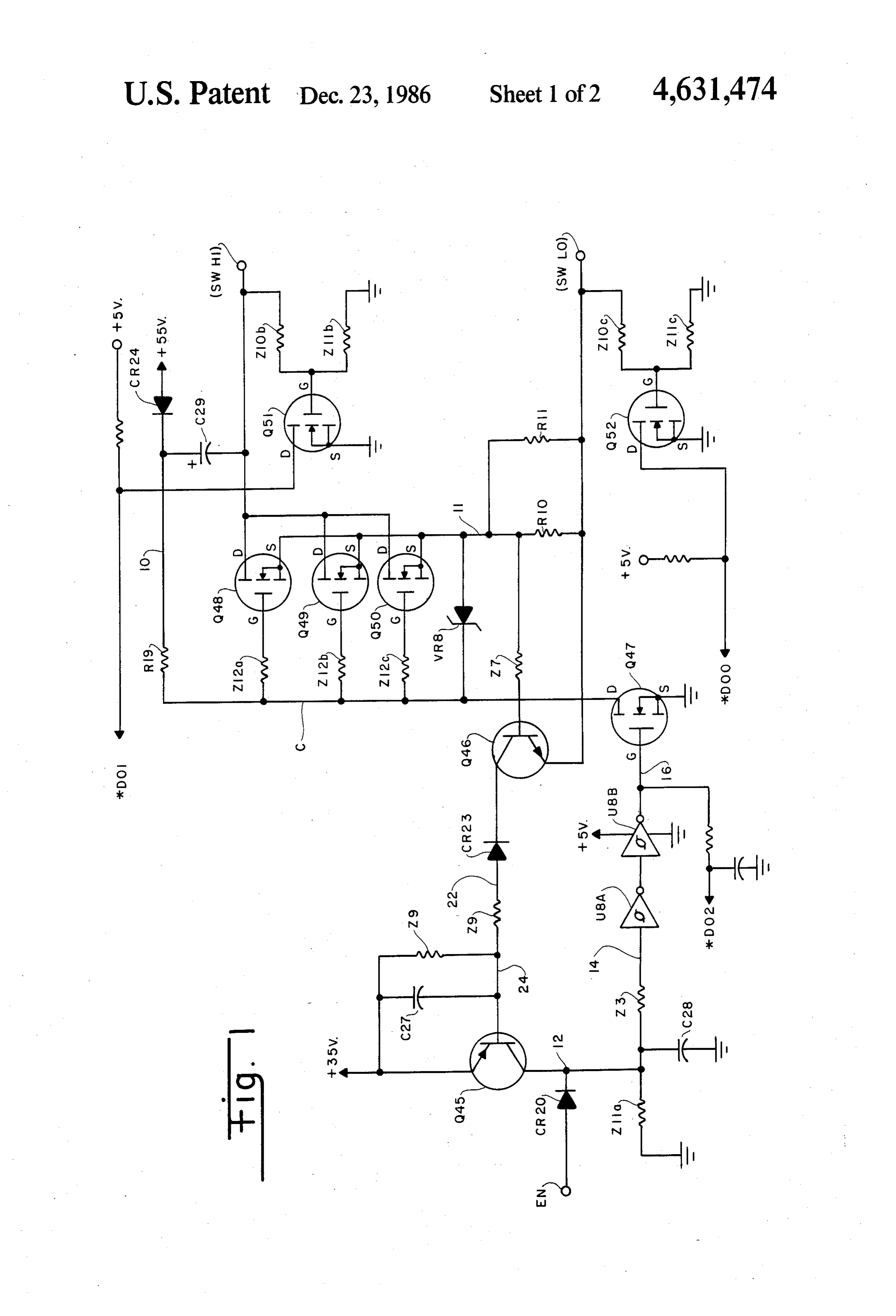
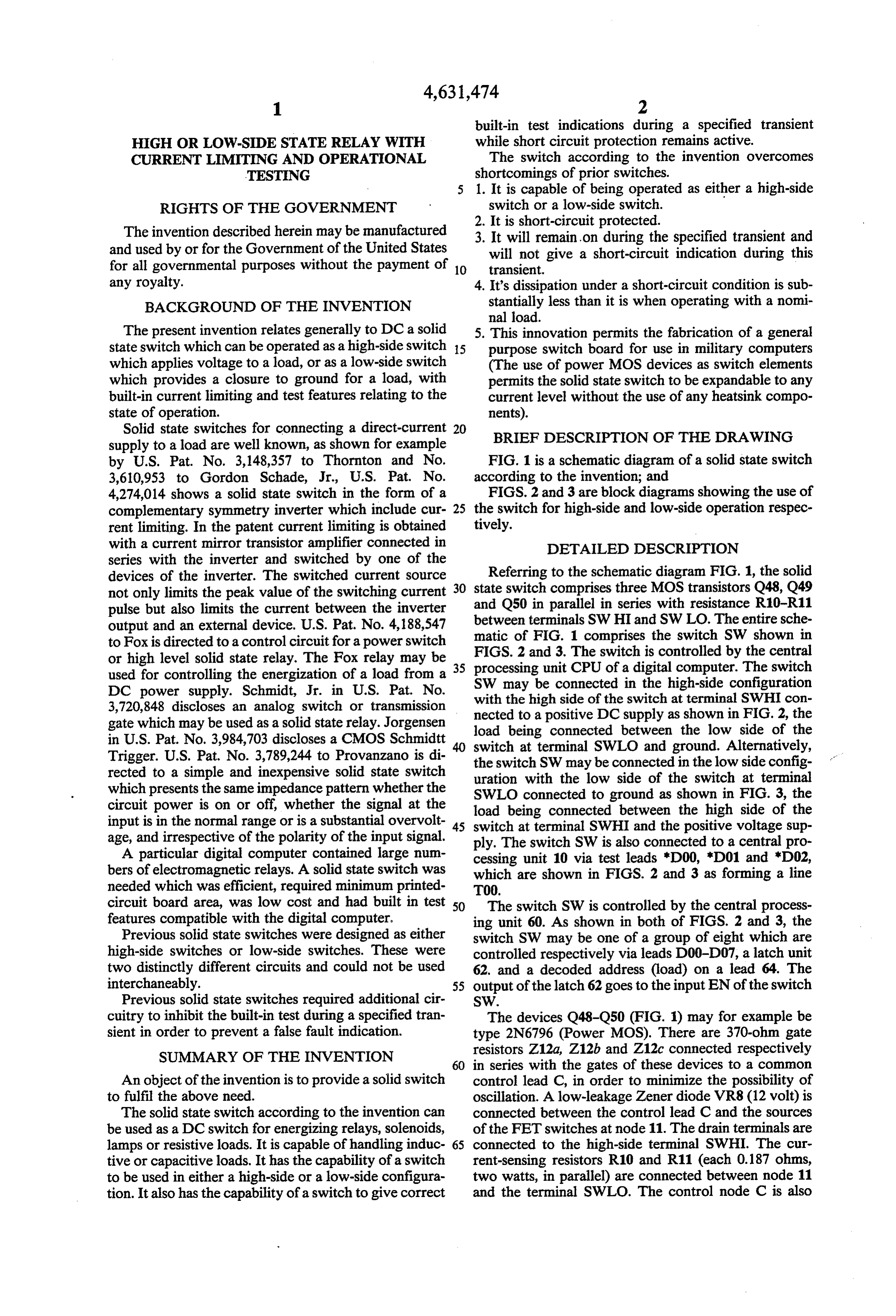
with a current mirror transistor amplifier connected in DETAILED DESCRIPTION series with the inverter and switched by one of the devices of the inverter. The switched current source Referring to the schematic diagram FIG. 1, the solid not only limits the peak value of the switching current 30 state switch comprises three MOS transistors Q48, Q49 pulse but also limits the current between the inverter and Q50 in parallel in series with resistance R10-R11 output and an external device. U.S. Pat. No. 4,188,547 betweenofterminals SWHI and SW LO. The entire sche to Fox is directed to a control circuit for a power switch matic FIG. 1 comprises the switch SW shown in or high level solid state relay. The Fox relay may be FIGS. 2 andunit 3. The switch is controlled by the central used for controlling the energization of a load from a processing
SW may be
CPU of a digital computer. The switch connected in the high-side configuration
DC power supply. Schmidt, Jr. in U.S. Pat. No.
3,720,848 discloses an analog switch or transmission with the high side of the switch at terminal SWHIcon gate which may be used as a solid state relay. Jorgensen nectedbeing to a positive DC supply as shown in FIG. 2, the in U.S. Pat. No. 3,984,703 discloses a CMOS Schmidtt load connected between the low side of the Trigger. U.S. Pat. No. 3,789,244 to Provanzano is di the switch SW may SWLO switch at terminal and ground. Alternatively, rected to a simple and inexpensive solid state switch uration with the low side of thein the be connected low side config switch at terminal which presents the same impedance pattern whether the circuit power is on or off, whether the signal at the SWLO load connected to ground as shown in FIG. 3, the being connected between the high side of the input is in the normal range or is a substantial overvolt 45 switch at terminal age, and irrespective of the polarity of the input signal. ply. The switch SWSWHI is and the positive voltage sup also connected to a central pro
A particular digital computer contained large num cessing unit 10 via test leads "D00, "D01 and "D02, bers of electromagnetic relays. A solid state switch was which are shown in FIGS. 2 and 3 as forming a line needed which was efficient, required minimum printed T00.
circuit board area, was low cost and had built in test 50 The switch SW is controlled by the central process features compatible with the digital computer, ing unit 60. As shown in both of FIGS. 2 and 3, the Previous solid state switches were designed as either switch SW may be one of a group of eight which are high-side switches or low-side switches. These were controlled respectively via leads D00-D07, a latch unit two distinctly different circuits and could not be used 62. and a decoded address (load) on a lead 64. The interchaneably. 55 output of the latch 62 goes to the input EN of the switch Previous solid state switches required additional cir SW.
cuitry to inhibit the built-in test during a specified tran The devices Q48-Q50 (FIG. 1) may for example be sient in order to prevent a false fault indication. type 2N6796 (Power MOS). There are 370-ohm gate SUMMARY OF THE INVENTION resistors Z12a, Z12b and Z12c connected respectively 60 in series with the gates of these devices to a common
An object of the invention is to provide a solid switch control lead C, in order to minimize the possibility of to fulfil the above need. oscillation. A low-leakage Zener diode VR8 (12 volt) is The solid state switch according to the invention can connected between the control lead C and the sources be used as a DC switch for energizing relays, solenoids, of the FET switches at node 11. The drain terminals are lamps or resistive loads. It is capable of handling induc 65 connected to the high-side terminal SWHI. The cur tive or capacitive loads. It has the capability of a switch rent-sensing resistors R10 and R11 (each 0.187 ohms, to be used in either a high-side or a low-side configura two watts, in parallel) are connected between node 11 tion. It also has the capability of a switch to give correct and the terminal SWLO. The control node C is also
Page 5
connected through a 56-kilohm resistor R19 to node 10. ground. The gate-to-source voltage for the switches This node 10 also connects to the cathode of a diode Q48-Q50 is controlled by the breakdown voltage of CR24, and to a 0.56-microfarad, 100-volt capacitor C29 Zener diode VR8. During an 80-volt transient as pre to form the bias supply for the FET switches, the anode scribed by a military standard MIL 704, the input volt of diode CR24 being connected to a 55-volt source, and age which is applied to terminal SWHI and is normally capacitor C29 to the terminal SWHI. 22 to 32 volts, surges to 80 volts for 100 milliseconds. The switch control input pin EN is coupled via a During this time capacitor C29 retains enough charge Schmitt Trigger circuit to the control node C. (Note to maintain the switch gate-to-source voltage and the that two Schmitt Trigger Inverters U8A and U8B such switch remains on.
as type MC14584 are used in tandem because CMOS 10 The switch operation in a low-side switch con Schmitt Trigger Buffers are not available). The input figuratioin (see FIG. 3) is identical to that described for circuit includes a diode CR20 connected from input a high-side switch.
terminal EN8 to a node 12. A 330-kilohm resistor Z11a The load current is sensed by resistors R10 and R11. and a 1.2-microfarad, 20-volt capacitor C28 are also When the current exceeds a prodetermined level the connected from node 12 to ground. A 10-kilohm resis 15 emitter-base tor Z3 isolates node 12 from the input of the Schmitt and transistorjunction of transistor Q46 is forward biased Trigger Inverter U8A. The output of the Schmitt Trig which charges capacitoron.
Q46 turns
This turns on transistor Q45 until a logical 1 is detected ger Inverter U8B is connected at node 16 to the gate of at the input of device U8A. The a MOS transistor Q47 (type 2N6796), whose drain is goes to a logical 0 and the outputoutput of device U8A connectged to the control node C, and whose source is logical 1, which turns on transistor Q47 and U8B
of device turns
off grounded.
A current limiting circuit comprises transistor ampli transistors Q48-Q50. These devices remain off until capacitor C28 discharges through resistor Z11a. Thus it fiers Q46 (type JANTX 2N3700) and Q45 (type can
JANTX 2N2907A). Transistor Q46 has its base con shortbecircuit seen that on/off duty cycle under overload or conditions can be controlled by resistor nected through a 120-ohm resistor Z7 to node 11, its 25 collector connected through a diode CR23 to a node 22, Z11a and capacitor C28 and the hysteresis of the Schmitt Trigger.
and its emitter connected to terminal SWLO. Transistor
Q45 has its base connected to a node 24, its collector byDuring a factor an 80-volt transient the load current increases of approximately 3. In a high-side configura connected to node 12, and its emitter connected to a tion the output +35-volt direct-current bias supply. A 2-kilohm resis 30 CR23 blocks thevoltage voltage of the switch is 80 volts. Diode and prevents the breakdown tor Z9 and a 0.1-microfarad capacitor C27 are con nected in parallel across the emitter-base junction of of transistors Q45 and Q46, both of these transistors are off, and normal operation of the switch continues. The transistor Q45. switch described has a rating of 5 amperes. For lower Test circuits to leads "D01 and D00 include MOS transistors Q51 and Q52 (both type 3N171). These test 35 current ratings transistor Q49 and/or Q50 and their base leads are connected to respective 10-kilohm pull-up resistors may be omitted.
resistors to a +5-volt bias supply, and also respectively Built-in test. to the drains of devices Q51 and Q52. The gate of the The circuit comprised of resistor Z10c, Z11c, and device Q51 is connected to a bias network comprised of transistor Q52 form a voltage detector with a threshold a one-megohm resistor Z10b and a 330-kilohm resistgor 40 of 6 volts. This threshold is controlled by the gate-to Z11b. Resistor Z10b connects the gate of device Q51 to source terminal SWHI; resistor Z11b connects the gate of de networkthreshold of transistor Q52 and the gain of the Z10c, Z11c. In a high-side configuration when vice Q51 to ground. The gate of device Q52 is similarly biased, the gate being connected to terminal SWLO the switch is on the potential at the terminal SWLO is through a one-megohm resistor and to ground through 45 28 volts (for a 28-volt system) and VGs of transistor Q52 a 330-kilohm resistor Z11c. The sources of devices Q51 is approximately 7 volts. This turns on transistor Q52 and Q52 are grounded. An optional test lead "DO2 is and provides a logical 0 at the terminal labeled "D00. connected via a resistor to node 16. This test lead is This discrete is read by the computer to determine filtered by a capacitor to ground. whether the switch is on, off, or shorted. The network In the system, a logical 1 is a positive voltage level 50 comprised of resistors Z10b, Z11b and transistor Q51 near 5 volts, and a logical 0 is a potential near ground. function in the same manner as that described for the
OPERATION
network Z10c, Z11c, Q52. The network Z10b, Z11b,
Q51 tells the CPU whether the input voltage to the
The switch is energized when a logical 0 is applied switch is present.
from terminal EN to the cathode of diode CR20. This 55 In a low-side switch configuration the feedback at causes the input of the CMOS Schmitt Trigger inverter terminal "D00 is normally a logical 1 unless there is no U8A to decay to a logical 0 and its output becomes a continuity between terminal SWLO and ground. In this logical 1-thus the output of device U8B is a logical 0. configuration the discrete "D01 provides the feedback Since the FET Q47 is a MOS device, the input impe to the CPU as to whether this switch is on, off or dance is high and the voltage at its gate is actually less 60 shorted.
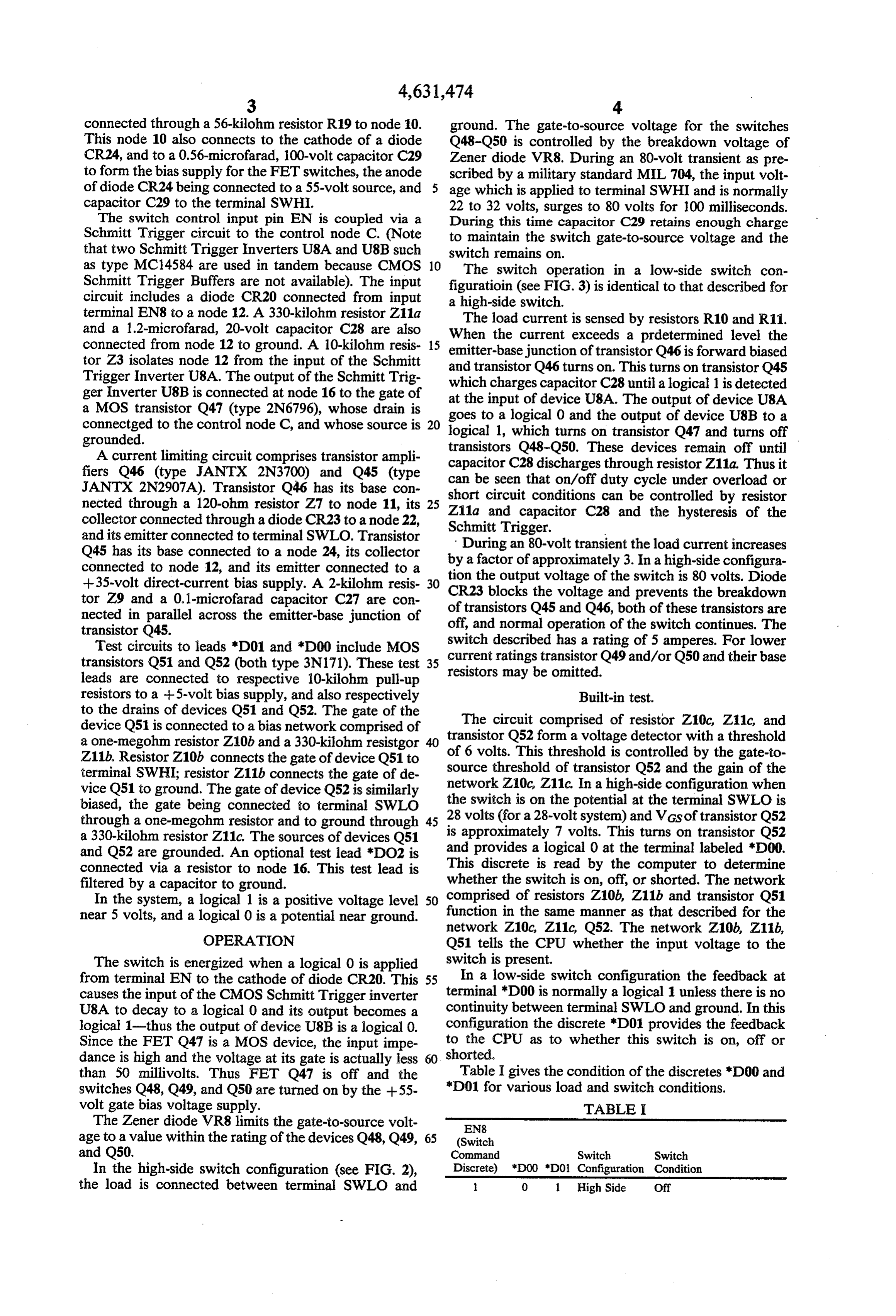
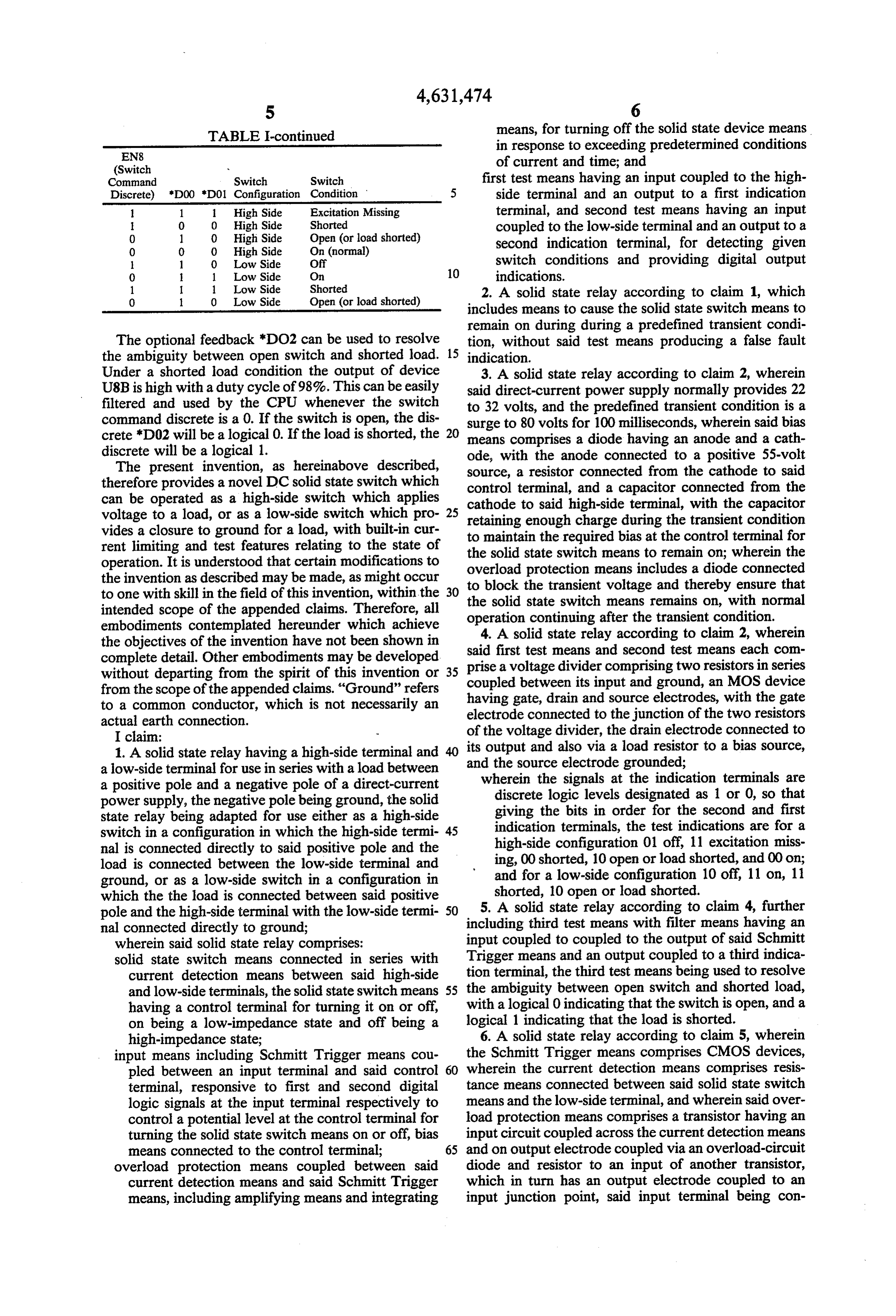
than 50 millivolts. Thus FET Q47 is off and the Table I gives the condition of the discretes "D00 and switches Q48, Q49, and Q50 are turned on by the +55 *D01 for various load and switch conditions. volt gate bias voltage supply. TABLE I The Zener diode VR8 limits the gate-to-source volt EN8 age to a value within the rating of the devices Q48, Q49, 65 (Switch and Q50. Command Switch Switch In the high-side switch configuration (see FIG. 2), Discrete) "D00 "D01 Configuration Condition the load is connected between terminal SWLO and 0 1 High Side Off
Page 6
TABLE I-continued means, for turning off the solid state device means
in response to exceeding predetermined conditions
(Switch of current and time; and
Command Switch Switch first test means having an input coupled to the high Discrete) "D00 'D01 Configuration Condition side terminal and an output to a first indication 1. 1 1 High Side Excitation Missing terminal, and second test means having an input
High Side
High Side
Shorted
Open (or load shorted) coupled to the low-side terminal and an output to a
O O 0 High Side On (normal) second indication terminal, for detecting given 0 Low Side Off switch conditions and providing digital output 0 1 Low Side On 10 indications.
1 1. 1 Low Side Shorted 2. A solid state relay according to claim 1, which 0. 1 0 Low Side Open (or load shorted) includes means to cause the solid state switch means to remain on during during a predefined transient condi
The optional feedback "DO2 can be used to resolve tion, without said test means producing a false fault the ambiguity between open switch and shorted load. 15 indication.
Under a shorted load condition the output of device 3. A solid state relay according to claim 2, wherein U8B is high with a duty cycle of 98%. This can be easily said direct-current power supply normally provides 22 filtered and used by the CPU whenever the switch to 32 volts, and the predefined transient condition is a command discrete is a 0. If the switch is open, the dis surge to 80 volts for 100 milliseconds, wherein said bias crete "D02 will be a logical 0. If the load is shorted, the 20 means comprises a diode having an anode and a cath discrete will be a logical 1. ode, with the anode connected to a positive 55-volt The present invention, as hereinabove described, source, a resistor connected from the cathode to said therefore provides a novel DC solid state switch which control terminal, and a capacitor connected from the can be operated as a high-side switch which applies cathode voltage to a load, or as a low-side switch which pro 25 retainingtoenough said high-side terminal, with the capacitor charge during the transient condition vides a closure to ground for a load, with built-in cur to maintain the required bias at the control terminal for rent limiting and test features relating to the state of the solid state switch means to remain on; wherein the operation. It is understood that certain modifications to overload protection means includes a diode connected the invention as described may be made, as might occur to block the to one with skill in the field of this invention, within the the solid statetransient
switch voltage and thereby ensure that means remains on, with normal intended scope of the appended claims. Therefore, all operation continuing after the transient condition. embodiments contemplated hereunder which achieve the objectives of the invention have not been shown in said first test means and second testto means 4. A solid state relay according claim 2, wherein each com complete detail. Other embodiments may be developed prise a voltage divider comprising two resistors without departing from the spirit of this invention or 35 coupled between its input and ground, an MOSindevice series from the scope of the appended claims. "Ground” refers having gate, drain and source electrodes, with the gate to a common conductor, which is not necessarily an electrode connected to the junction of the two resistors actual earth connection.
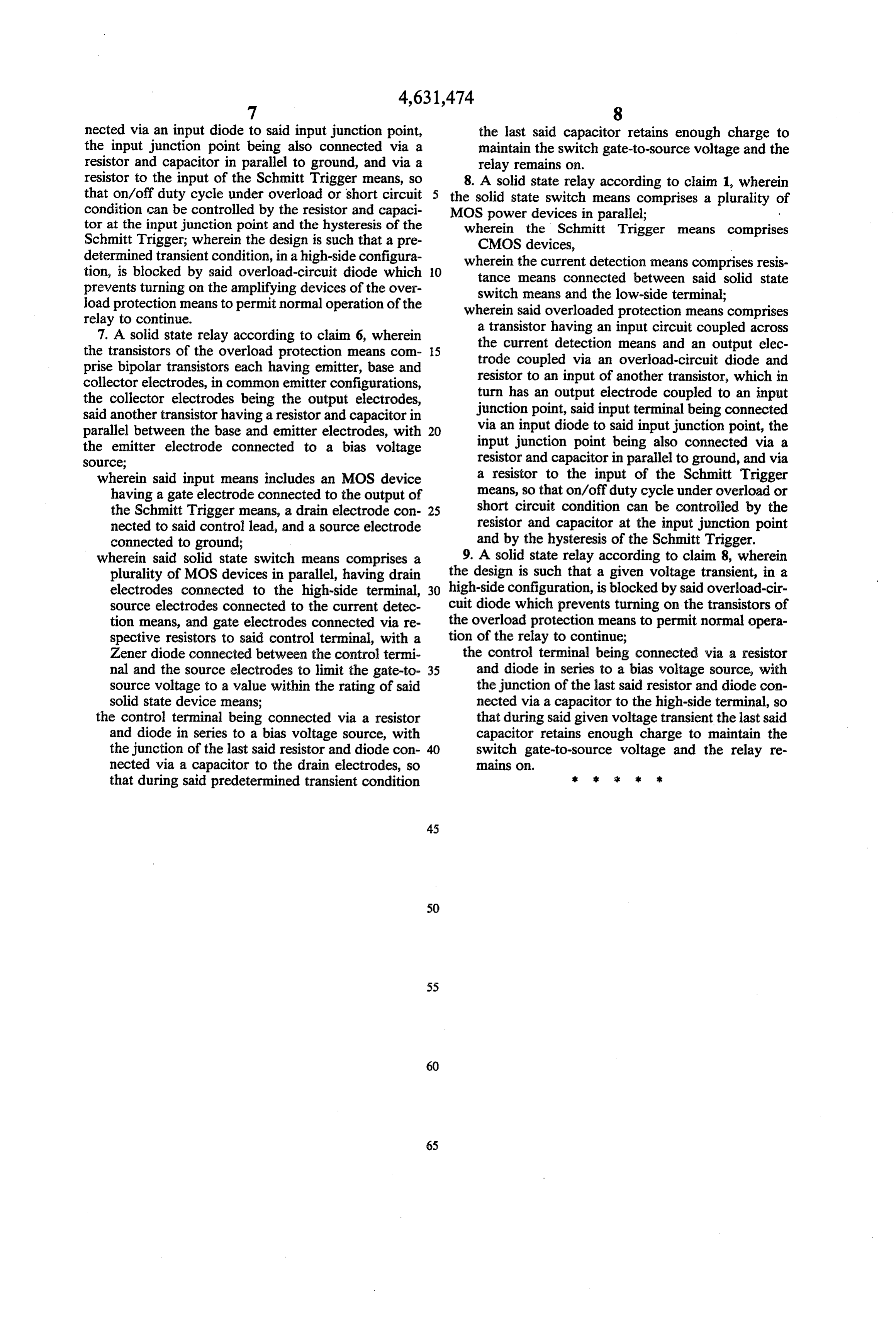
I claim: n of the voltage divider, the drain electrode connected to 1. A solid state relay having a high-side terminal and its output and also via a load resistor to a bias source, a low-side terminal for use in series with a load between and the source electrode grounded; a positive pole and a negative pole of a direct-current wherein the signals at the indication terminals are power supply, the negative pole being ground, the solid discrete logic levels designated as 1 or 0, so that state relay being adapted for use either as a high-side giving the bits in order for the second and first switch in a configuration in which the high-side termi 45 indication terminals, the test indications are for a nal is connected directly to said positive pole and the high-side configuration 01 off, 11 excitation miss load is connected between the low-side terminal and ing, 00 shorted, 10 open or load shorted, and 00 on; ground, or as a low-side switch in a configuration in and for a low-side configuration 10 off, 11 on, 11 which the the load is connected between said positive shorted, 10 open or load shorted. pole and the high-side terminal with the low-side termi 50 5. A solid state relay according to claim 4, further nal connected directly to ground; including third test means with filter means having an wherein said solid state relay comprises: input coupled to coupled to the output of said Schmitt solid state switch means connected in series with Trigger means and an output coupled to a third indica current detection means between said high-side tion terminal, the third test means being used to resolve and low-side terminals, the solid state switch means 55 the ambiguity between open switch and shorted load, having a control terminal for turning it on or off, with a logical 0 indicating that the switch is open, and a on being a low-impedance state and off being a logical 1 indicating that the load is shorted. high-impedance state; 6. A solid state relay according to claim 5, wherein input means including Schmitt Trigger means cou the Schmitt Trigger means comprises CMOS devices, pled between an input terminal and said control 60 wherein the current detection means comprises resis terminal, responsive to first and second digital tance means connected between said solid state switch logic signals at the input terminal respectively to means and the low-side terminal, and wherein said over control a potential level at the control terminal for load protection means comprises a transistor having an turning the solid state switch means on or off, bias input circuit coupled across the current detection means means connected to the control terminal; 65 and on output electrode coupled via an overload-circuit overload protection means coupled between said diode and resistor to an input of another transistor, current detection means and said Schmitt Trigger which in turn has an output electrode coupled to an means, including amplifying means and integrating input junction point, said input terminal being con
Page 7
nected via an input diode to said input junction point, the last said capacitor retains enough charge to the input junction point being also connected via a maintain the switch gate-to-source voltage and the resistor and capacitor in parallel to ground, and via a relay remains on.
resistor to the input of the Schmitt Trigger means, so 8. A solid state relay according to claim 1, wherein that on/off duty cycle under overload or short circuit 5 the solid state switch means comprises a plurality of condition can be controlled by the resistor and capaci MOS power devices in parallel;
tor at the input junction point and the hysteresis of the wherein the Schmitt Trigger means comprises Schmitt Trigger; wherein the design is such that a pre CMOS devices, determined transient condition, in a high-side configura wherein the current detection means comprises resis tion, is blocked by said overload-circuit diode which 10 tance means connected between said solid state prevents turning on the amplifying devices of the over switch means and the low-side terminal; load protection means to permit normal operation of the wherein said overloaded protection means comprises relay to continue. a transistor having an input circuit coupled across 7. A solid state relay according to claim 6, wherein the current detection means and an output elec the transistors of the overload protection means com 15 trode coupled via an overload-circuit diode and prise bipolar transistors each having emitter, base and resistor to an input of another transistor, which in collector electrodes, in common emitter configurations, turn has an output electrode coupled to an input the collector electrodes being the output electrodes, junction point, said input terminal being connected said another transistor having a resistor and capacitor in via an input diode to said input junction point, the parallel between the base and emitter electrodes, with 20 input junction point being also connected via a the emitter electrode connected to a bias voltage resistor and capacitor in parallel to ground, and via Source;
wherein said input means includes an MOS device a resistor to the input of the Schmitt Trigger having a gate electrode connected to the output of means, so that on/off duty cycle under overload or the Schmitt Trigger means, a drain electrode con 25 short circuit condition can be controlled by the nected to said control lead, and a source electrode resistor and capacitor at the input junction point connected to ground; and by the hysteresis of the Schmitt Trigger. wherein said solid state switch means comprises a 9. A solid state relay according to claim 8, wherein plurality of MOS devices in parallel, having drain the design is such that a given voltage transient, in a electrodes connected to the high-side terminal, 30 high-side configuration, is blocked by said overload-cir source electrodes connected to the current detec cuit diode which prevents turning on the transistors of tion means, and gate electrodes connected via re the overload protection means to permit normal opera spective resistors to said control terminal, with a tion of the relay to continue;
Zener diode connected between the control termi the control terminal being connected via a resistor nal and the source electrodes to limit the gate-to 35 and diode in series to a bias voltage source, with source voltage to a value within the rating of said the junction of the last said resistor and diode con solid state device means; nected via a capacitor to the high-side terminal, so the control terminal being connected via a resistor that during said given voltage transient the last said and diode in series to a bias voltage source, with capacitor retains enough charge to maintain the the junction of the last said resistor and diode con switch gate-to-source voltage and the relay re nected via a capacitor to the drain electrodes, so mains on.
that during said predetermined transient condition k 32 k k
Provenance
- Collection
- Cited prior art
- Original PDF
- patentimages.storage.googleapis.com →
- Filed
- 1984-07-11
- Pages
- 7
- Method
- pdftotext (the PDF's own text layer) + pdftoppm 300dpi page scans
- Source
- Google Patents bibliographic record
- Granted
- 1986-12-23
- Inventors
- Carlisle R. Dolland; United States Department of the Air Force
- Transcribed from
- patentimages.storage.googleapis.com →