patent · US4628905
Solar selective surface coating
16 December 1986
Page 1 — bibliographic record
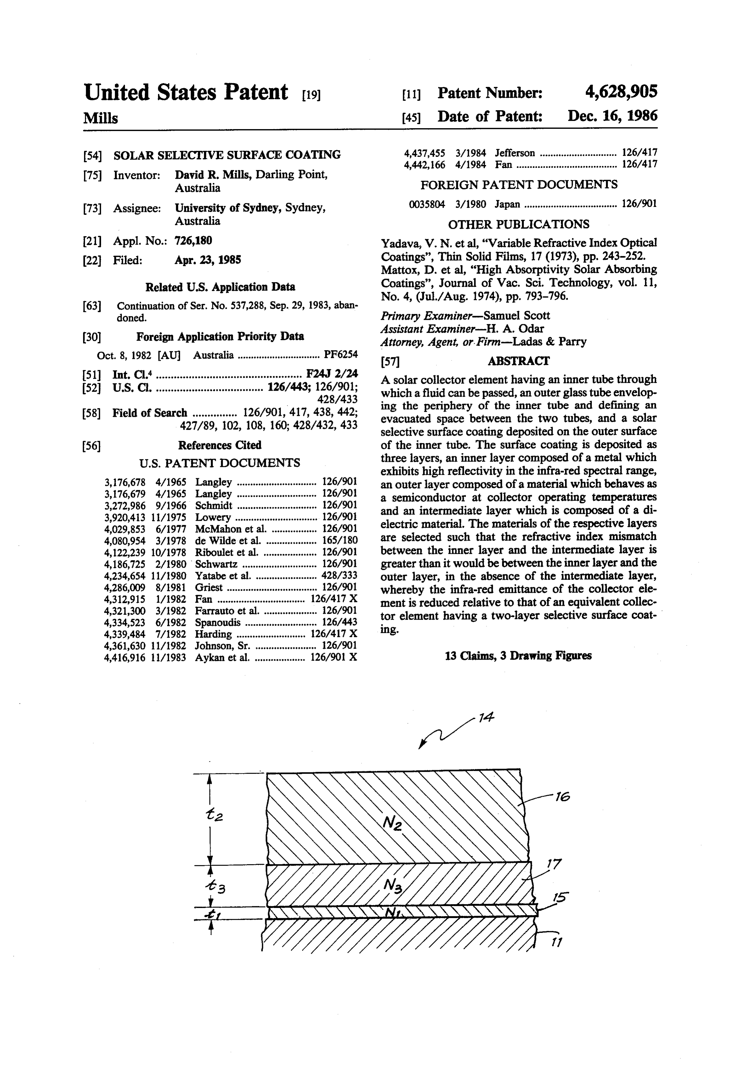
United States Patent (19) 11 Patent Number: 4,628,905 Mills (45) Date of Patent: Dec. 16, 1986 (54) SOLAR SELECTIVESURFACE COATING 4,437,455 3/1984 Jefferson ............................. 126/417 4,442,66 4/1984 Fan ...................................... 126/417 75 Inventor: David R. Mills, Darling Point,
Australia FOREIGN PATENT DOCUMENTS 73) Assignee: University of Sydney, Sydney, 0035804 3/1980 Japan ................................... 126/901 Australia OTHER PUBLICATIONS 21) Appl. No.: 726,180 Yadava, V. N. etal, "Variable Refractive Index Optical 22 Filed: Apr. 23, 1985 Coatings', Thin Solid Films, 17 (1973), pp. 243-252. Mattox, D. et al, "High Absorptivity Solar Absorbing
Related U.S. Application Data Coatings', Journal of Vac. Sci. Technology, vol. 11,
I63 Continuation of Ser. No. 537,288, Sep. 29, 1983, aban doned. Primary Examiner-Samuel Scott
Assistant Examiner-H. A. Odar (30) Foreign Application Priority Data Attorney, Agent, or Firm-Ladas & Parry Oct. 8, 1982 AU Australia............................... PF6254 57 ABSTRACT 51 Int. Cl."................................................. F24J 2/24 A solar collector element having an inner tube through 52 U.S. C. .................................... 126/443; 126/901; which a fluid can be passed, an outer glass tube envelop 428/433 ing the periphery of the inner tube and defining an 58) Field of Search ............... 126/901, 417,438, 442; evacuated space between the two tubes, and a solar 427/89, 102, 108, 160; 428/432, 433 selective surface coating deposited on the outer surface (56) References Cited of the inner tube. The surface coating is deposited as
exhibits high reflectivity in the infra-red spectral range, 3,176,678 4/1965 Langley ... ... 126/90 an outer layer composed of a material which behaves as 3,176,679 4/1965 Langley ... ... 126/901 a semiconductor at collector operating temperatures 3,272,986 9/1966 Schmidt ... ... 126/901 3,920,413 11/1975 Lowery ................ ... 126/901 and an intermediate layer which is composed of a di 4,029,853 6/1977 McMahon et al. ... ... 126/901 electric material. The materials of the respective layers 4,080,954 3/1978 de Wilde et al. ..... ... 165/180 are selected such that the refractive index mismatch 4,122,239 10/1978 Riboulet et al... ... 126/901 between the inner layer and the intermediate layer is 4,186,725 2/1980 Schwartz .......... ... 126/90 greater than it would be between the inner layer and the 4,234,654 11/1980 Yatabe et al. . ... 428/333 outer layer, in the absence of the intermediate layer, 4,286,009 8/1981 Griest ........... vw w w A 126/901 whereby the infra-red emittance of the collector ele 4,312,915 1/1982 Fan ................... ... 126/417 X ment is reduced relative to that of an equivalent collec 4,321,300 3/1982 Farrauto et al ... 126/901 4,334,523 6/1982 Spanoudis ........................... 126/443 tor element having a two-layer selective surface coat 4,339,484 7/1982 Harding ........ ... 26/417 X ling.
4,361,630 1 1/1982 Johnson, Sr. ....................... 126/901 4,416,916 11/1983 Aykan et al. ................... 126/901 X 13 Claims, 3 Drawing Figures
Page 2
Drawing sheet — no readable text.
Page 3
Drawing sheet — no readable text.
Page 4
for normal incident radiation over at least a major por
SOLAR SELECTIVESURFACE COATING tion of the infra-red spectral range.
With the above defined surface coating structure, the
This is a continuation of co-pending application Ser. refractive index mismatch between the inner layer and No. 537,288 filed on Sept. 29, 1983, now abandoned. 5 the intermediate layer is greater than it would be be tween the inner layer and the outer layer (in the absence
FIELD OF THE INVENTION of the intermediate layer) and, therefore, less infra-red This invention relates to a solar selective surface radiation will be coupled out of the inner layer. Stated coating for absorber surfaces which are employed in in an alternative way, a higher value of infra-red reflec solar collectors. In particular, the invention is directed 10 tance is obtained at the interface of the inner and inter mediate layers than would be attainable at the interface to a solar selective surface coating which includes a of a two-layer solar selective surface coating. refractive index mismatch layer for the purpose of re ducing infra-red emittance. PREFERRED FEATURES OF THE INVENTION BACKGROUND OF THE INVENTION 15 The intermediate layer preferably is composed of a Solar selective surface coatings known in the art dielectric material which is highly transparent to infra red radiation (i.e., having k3 approximately equal to 0) usually comprise an outer layer of a material which and which has a real refractive index n3 less than about absorbs strongly in the solar energy spectral range but 2.5. Suitable such materials include magnesium fluoride, which is transparent to infra-red radiation. In the inter 20 magnesium oxide, titanium oxide, aluminium oxide, est of reducing thermal losses, the outer layer is depos silica, quartz and carbon.
ited on an inner layer of a material which provides high The outer layer preferably is composed of a material reflectivity and, hence, low emissivity in the infra-red which behaves as a semiconductor at collector operat spectrum. A typical such selective surface coating is ing temperatures. Such material may have a monocrys disclosed in U.S. Pat. No. 4,339,484, the surface coating 25 talline, polycrystalline or amorphous structure and may comprising a metal-carbide solar energy absorptive comprise, for example, germanium, a germanium-sili outer layer and a copper infra-red reflective base coat con alloy, silicon carbide, lead sulphide, boron or, in the ing. The metal-carbide absorptive layer is graded such case of surface coatings to be employed in relatively that it has a high carbide-to-metal ratio near its outer low temperature collector systems, tellurium com surface and a high metal-to-carbide ratio adjacent the 30 pounds. The material may alternatively be in the form interface between the absorptive surface and the reflec of a cermet and, in such case, the material forming the tive base coating. dielectric matrix of the cermet may be the same as or A problem that is inherent in the traditional selective different from the dielectric material which forms the surface coatings is that the emissivity of the total surface intermediate layer of the surface coating. coating is much higher than the emissivity of the reflec 35 Also, the outer layer preferably is graded, either geo tive base layer alone. One of the major reasons for this metrically or in terms of its composition, such that its is that the emissivity of a material increases if the optical refractive index to solar radiation increases with in constants of a superimposed medium are different from creasing depth of the layer and such that the maximum those of free space, and this normally is the case with 40 (real and imaginary) refractive indices (n2 and k2) occur materials that are employed for absorptive surface coat adjacent the interface with the intermediate layer. Geo ings. Such materials, if semiconductors, may have re metrical chemically grading (i.e. texturing) may be achieved by etching the outer layer of the surface coat fractive indices in the order of 2 to 10 times greater than that of free space and, therefore, the coupling of infra ing.Furthermore, the outer layer may be constituted by a red radiation across the metal-semiconductor interface may be significantly greater than that of a metal-air 45 the number of sub-layers and include interference layers for interface. purpose of providing destructive interference to solar radiation. Similarly, the intermediate layer may
SUMMARY OF THE INVENTION include a number of sub-layers, but preliminary investi gations
The present invention seeks to alleviate this problem 50 from such tend to indicate that no benefit is to be gained by providing a solar selective surface coating which that, allowing a structure. However, the point to be noted is comprises at least three layers; an inner layer composed surface structure for the possibility of sub-layers, the total of a material having high reflectivity and, hence, low layers. may, in fact, include more than three emissivity in the infra-red spectral range, an outer layer The inner layer preferably comprises a metal, such as composed of a material which is absorptive of energy in 55 copper, aluminium, molybdenum, silver or gold which the solar energy spectral range and which is substan exhibits a high reflectance to infra-red radiation, and tially transparent to infra-red radiation, and an interme such metal layer, when composed of copper, would diate layer composed of a maerial which is substantially normally be deposited to a thickness of at least transparent to infra-red radiation. The inner, outer and 0.10x10⁻⁶ m.
intermediate layer materials have complex refractive 60 The intermediate layer preferably is deposited to a indices (n1-ik), (n2-ik2) and (n3-ik3) respectively minimum thickness of 0.15x10⁻⁶ m., and the outer and the materials are selected to satisfy the relationship layer would normally be deposited to produce a solar energy absorptive layer having a thickness in the order
65 The inner, intermediate and outer layer materials
which are employed in any given coating desirably should have coefficients of thermal expansion which are approximately equal, in order that the risk of differential
Page 5
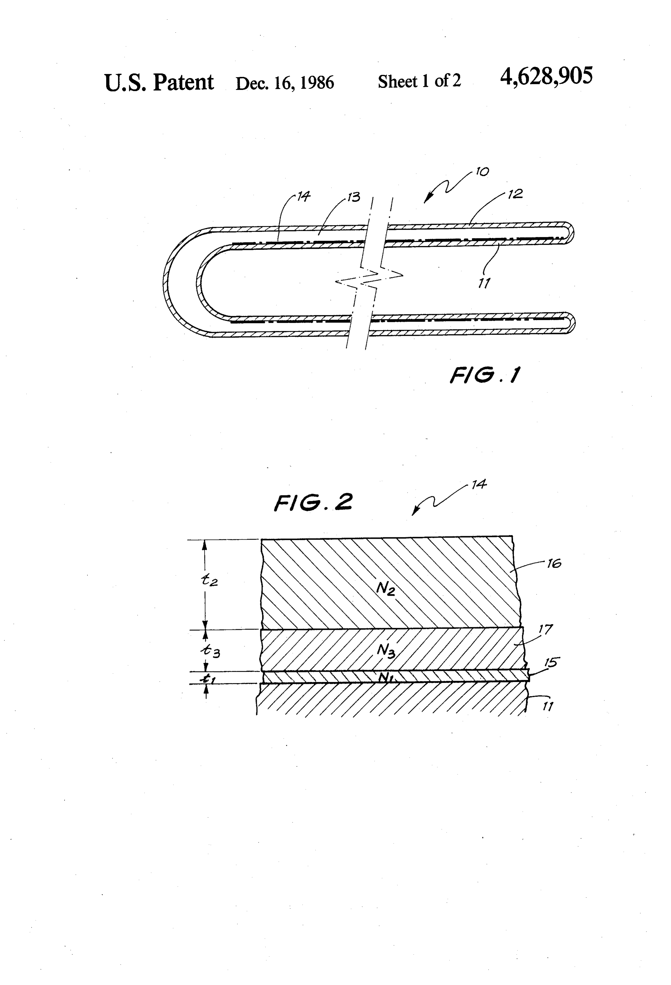
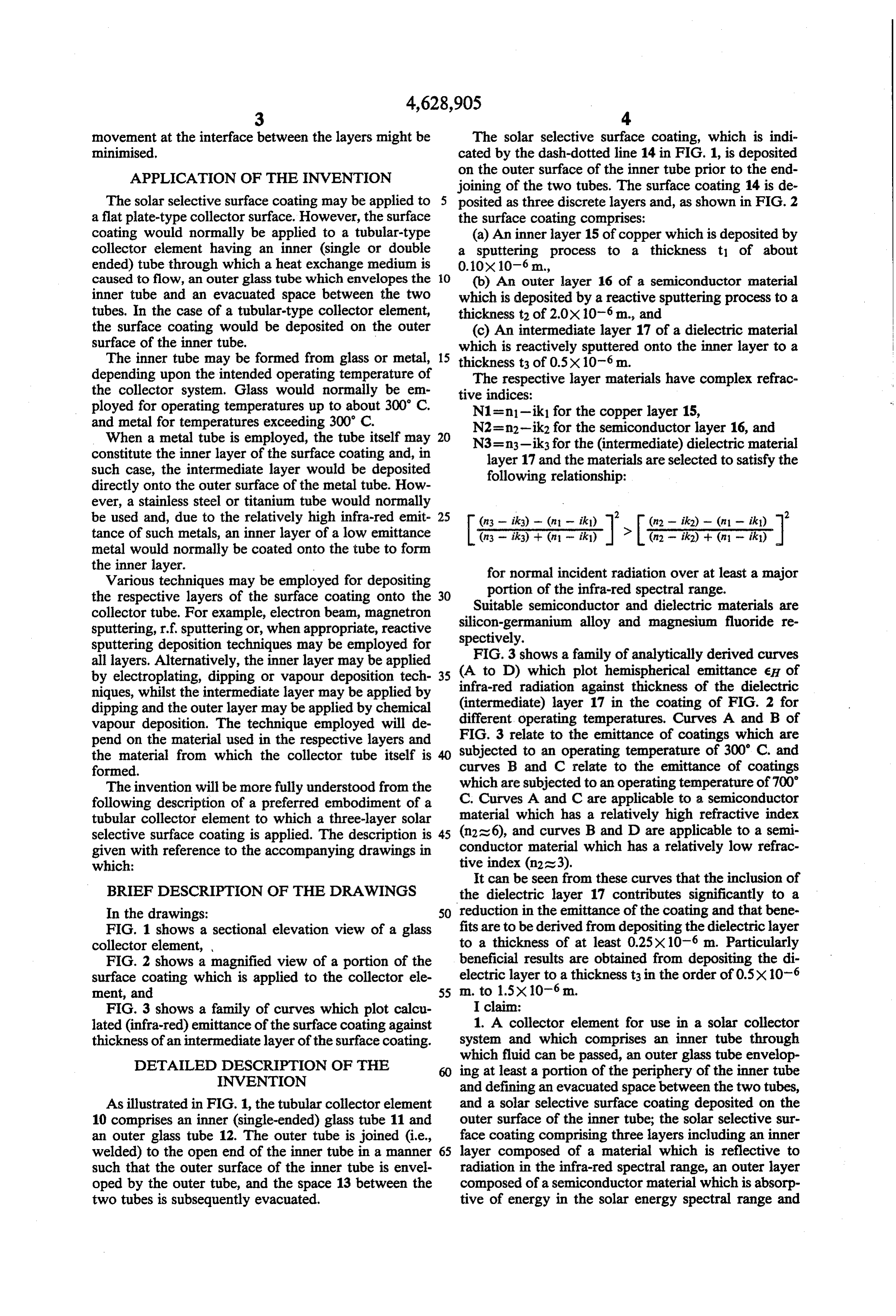
movement at the interface between the layers might be The solar selective surface coating, which is indi minimised. cated by the dash-dotted line 14 in FIG. 1, is deposited APPLICATION OF THE INVENTION on the outer surface of the inner tube prior to the end joining of the two tubes. The surface coating 14 is de
The solar selective surface coating may be applied to 5 posited as three discrete layers and, as shown in FIG. 2 a flat plate-type collector surface. However, the surface the surface coating comprises:
coating would normally be applied to a tubular-type (a) An inner layer 15 of copper which is deposited by collector element having an inner (single or double a sputtering process to a thickness t of about ended) tube through which a heat exchange medium is 0.10x10⁻⁶ m., caused to flow, an outer glass tube which envelopes the O (b) An outer layer 16 of a semiconductor material inner tube and an evacuated space between the two which is deposited by a reactive sputtering process to a tubes. In the case of a tubular-type collector element, thickness t? of 2.0x10⁻⁶ m., and the surface coating would be deposited on the outer (c) An intermediate layer 17 of a dielectric material surface of the inner tube. which is reactively sputtered onto the inner layer to a The inner tube may be formed from glass or metal, 15 thickness t3 of 0.5x10⁻⁶ m.
depending upon the intended operating temperature of The respective layer materials have complex refrac the collector system. Glass would normally be em tive indices:
ployed for operating temperatures up to about 300 C. N1=n-ik1 for the copper layer 15, and metal for temperatures exceeding 300° C. N2=n2-ik2 for the semiconductor layer 16, and When a metal tube is employed, the tube itself may N3=n3-ik3 for the (intermediate) dielectric material constitute the inner layer of the surface coating and, in layer 17 and the materials are selected to satisfy the such case, the intermediate layer would be deposited following relationship:
directly onto the outer surface of the metal tube. How ever, a stainless steel or titanium tube would normally be used and, due to the relatively high infra-red emit 25 (n3 -ika) - (n1-iki) (n2 - ik2) - (n1-iki) ' tance of such metals, an inner layer of a low emittance ii) - G - is > 0, is ( - i) metal would normally be coated onto the tube to form the inner layer. for normal incident radiation over at least a major Various techniques may be employed for depositing portion of the infra-red spectral range. the respective layers of the surface coating onto the Suitable semiconductor and dielectric materials are collector tube. For example, electron beam, magnetron silicon-germanium alloy and magnesium fluoride re sputtering, r.f. sputtering or, when appropriate, reactive sputtering deposition techniques may be employed for spectively.
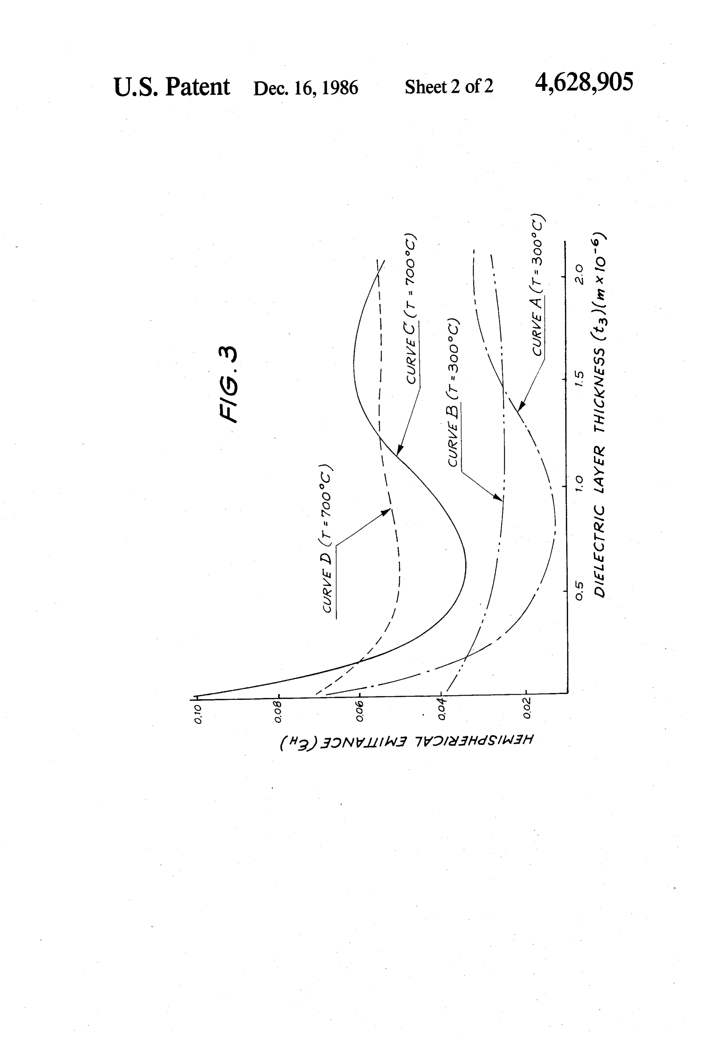
all layers. Alternatively, the inner layer may be applied FIG. 3 shows a family of analytically derived curves by electroplating, dipping or vapour deposition tech 35 (A to D) which plot hemispherical emittance eH of niques, whilst the intermediate layer may be applied by infra-red radiation against thickness of the dielectric dipping and the outer layer may be applied by chemical (intermediate) layer 17 in the coating of FIG. 2 for vapour deposition. The technique employed will de different operating temperatures. Curves A and B of pend on the material used in the respective layers and FIG. 3 relate to the emittance of coatings which are the material from which the collector tube itself is subjected to an operating temperature of 300° C. and formed. curves B and C relate to the emittance of coatings The invention will be more fully understood from the which are subjected to an operating temperature of 700 following description of a preferred embodiment of a C. Curves A and C are applicable to a semiconductor tubular collector element to which a three-layer solar material which has a relatively high refractive index selective surface coating is applied. The description is 45 (n2s6), and curves B and D are applicable to a semi given with reference to the accompanying drawings in conductor material which has a relatively low refrac which: tive index (n2at3).
It can be seen from these curves that the inclusion of
BRIEF DESCRIPTION OF THE DRAWINGS the dielectric layer 17 contributes significantly to a In the drawings: 50 reduction in the emittance of the coating and that bene FIG. 1 shows a sectional elevation view of a glass fits are to be derived from depositing the dielectric layer collector element, to a thickness of at least 0.25x10⁻⁶ m. Particularly FIG. 2 shows a magnified view of a portion of the beneficial results are obtained from depositing the di surface coating which is applied to the collector ele electric layer to a thickness t in the order of 0.5x10⁻⁶ ment, and 55 m. to 1.5x10⁻⁶ m.
FIG. 3 shows a family of curves which plot calcu I claim:
lated (infra-red) emittance of the surface coating against 1. A collector element for use in a solar collector thickness of an intermediate layer of the surface coating. system and which comprises an inner tube through
DETALED DESCRIPTION OF THE
which fluid can be passed, an outer glass tube envelop
INVENTION
ing at least a portion of the periphery of the inner tube and defining an evacuated space between the two tubes,
As illustrated in FIG. 1, the tubular collector element and a solar selective surface coating deposited on the 10 comprises an inner (single-ended) glass tube 11 and outer surface of the inner tube; the solar selective sur an outer glass tube 12. The outer tube is joined (i.e., face coating comprising three layers including an inner welded) to the open end of the inner tube in a manner 65 layer composed of a material which is reflective to such that the outer surface of the inner tube is envel radiation in the infra-red spectral range, an outer layer oped by the outer tube, and the space 13 between the composed of a semiconductor material which is absorp two tubes is subsequently evacuated. tive of energy in the solar energy spectral range and
Page 6
which is substantially transparent to infra-red radiation, the refractive index to solar radiation increases with and an intermediate layer composed of a dielectric ma increasing depth of the layer.
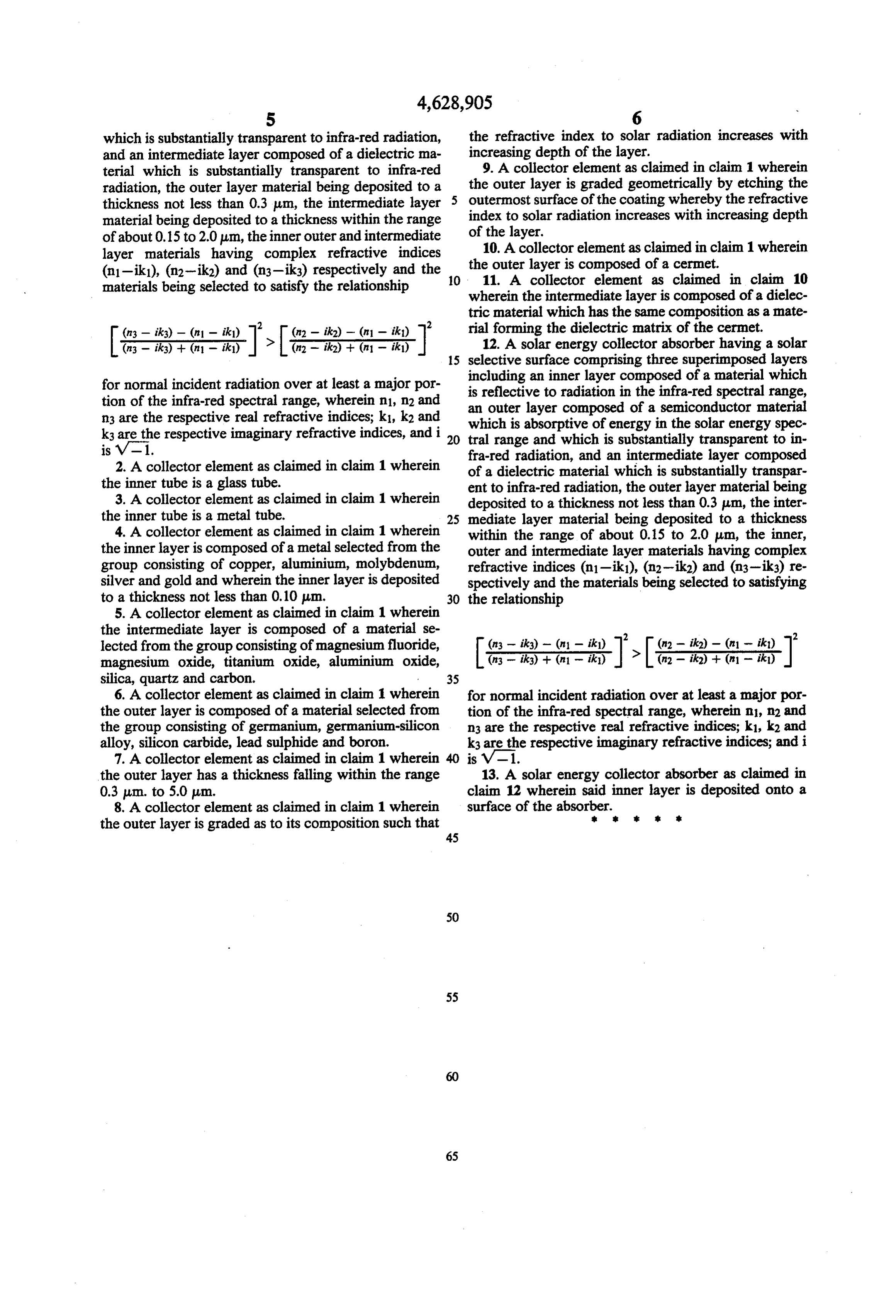
terial which is substantially transparent to infra-red 9. A collector element as claimed in claim 1 wherein radiation, the outer layer material being deposited to a the outer layer is graded geometrically by etching the thickness not less than 0.3 um, the intermediate layer 5 outermost surface of the coating whereby the refractive material being deposited to a thickness within the range index to solar radiation increases with increasing depth of about 0.15 to 2.0 um, the inner outer and intermediate of the layer.
layer materials having complex refractive indices the10.outer A collector element as claimed in claim 1 wherein (n1-iki), (n2-ik2) and (n3-ik3) respectively and the 10 11. A layer is composed of a cermet. collector element as claimed in claim 10 materials being selected to satisfy the relationship wherein the intermediate layer is composed of a dielec tric material which has the same composition as a mate rial forming the dielectric matrix of the cermet.
(n2 - ik2) + (n - ik) 12. A solar energy collector absorber having a solar 15 selective surface comprising three superimposed layers for normal incident radiation over at least a major por including
an inner layer composed of a material which reflective to radiation in the infra-red spectral range, tion of the infra-red spectral range, wherein n1, n2 and an outer layer composed of a semiconductor material n3 are the respective real refractive indices; k1,k2 and which is absorptive k3 are the respective imaginary refractive indices, and i 20 tral range and whichofisenergy in the solar energy spec substantially transparent to in is V-1. fra-red radiation, and an intermediate layer composed 2. A collector element as claimed in claim 1 wherein of a dielectric material which is substantially transpar the inner tube is a glass tube. ent to infra-red radiation, the outer layer material being 3. A collector element as claimed in claim 1 wherein deposited to a thickness not less than 0.3 um, the inter the inner tube is a metal tube. 25 mediate layer material being deposited to a thickness 4. A collector element as claimed in claim 1 wherein within the range of about 0.15 to 2.0 um, the inner, the inner layer is composed of a metal selected from the outer and intermediate layer materials having complex group consisting of copper, aluminium, molybdenum, refractive indices (n1-ik1), (n2-ik2) and (n3-ik3) re silver and gold and wherein the inner layer is deposited spectively and the materials being selected to satisfying to a thickness not less than 0.10 Jum. 30 the relationship 5. A collector element as claimed in claim 1 wherein the intermediate layer is composed of a material se 2 2 lected from the group consisting of magnesium fluoride, (n2 - ik2) - (n1 - ik) magnesium oxide, titanium oxide, aluminium oxide, silica, quartz and carbon. 35
6. A collector element as claimed in claim 1 wherein for normal incident radiation over at least a major por the outer layer is composed of a material selected from tion of the infra-red spectral range, wherein n, n2 and the group consisting of germanium, germanium-silicon n3 are the respective real refractive indices; k1,k2 and alloy, silicon carbide, lead sulphide and boron. k3 are the respective imaginary refractive indices; and i 7. A collector element as claimed in claim 1 wherein 40 is V-1.
the outer layer has a thickness falling within the range 13. A solar energy collector absorber as claimed in 0.3 um. to 5.0 pum. claim 12 wherein said inner layer is deposited onto a 8. A collector element as claimed in claim 1 wherein surface of the absorber.
the outer layer is graded as to its composition such that
Provenance
- Collection
- Cited prior art
- Original PDF
- patentimages.storage.googleapis.com →
- Filed
- 1985-04-23
- Pages
- 6
- Method
- pdftotext (the PDF's own text layer) + pdftoppm 300dpi page scans
- Source
- Google Patents bibliographic record
- Granted
- 1986-12-16
- Inventors
- David R. Mills; University of Sydney
- Transcribed from
- patentimages.storage.googleapis.com →