patent · US4152624
Molded LED indicator
1 May 1979
Page 1 — bibliographic record
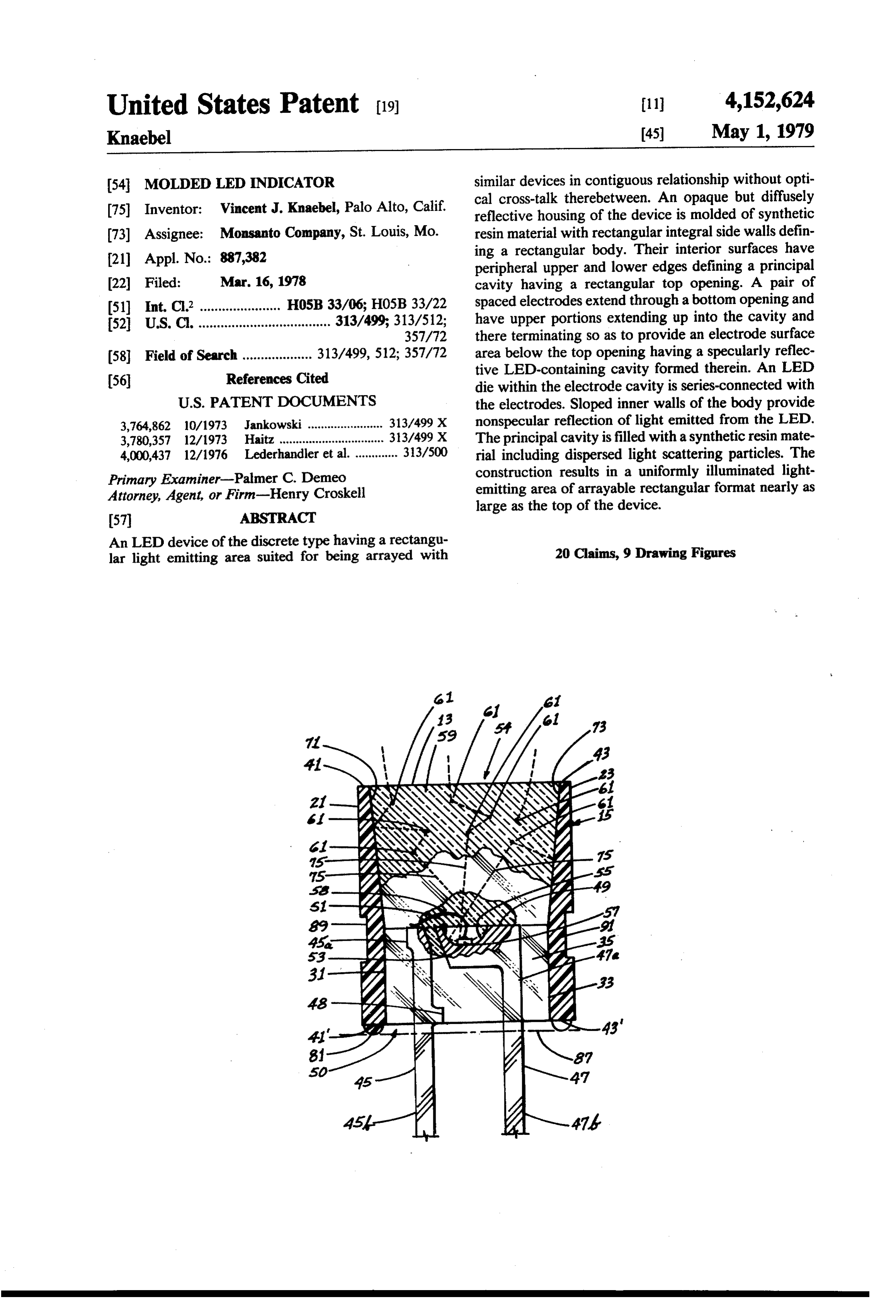
United States Patent (19) 11 4,152,624 Knaebel (45) May 1, 1979 54 MOLDED LED INDICATOR similar devices in contiguous relationship without opti (75) Inventor: Vincent J. Knaebel, Palo Alto, Calif.
cal cross-talk therebetween. An opaque but diffusely reflective housing of the device is molded of synthetic 73) Assignee: Monsanto Company, St. Louis, Mo. resin material with rectangular integral side walls defin (21) Appl. No.: 887,382 ing a rectangular body. Their interior surfaces have peripheral upper and lower edges defining a principal 22 Filed: Mar. 16, 1978 cavity having a rectangular top opening. A pair of 51) Int. Cl. ...................... H05B33/06; H05B33/22 spaced electrodes extend through a bottom opening and 52 U.S. C. .................................... 313/499; 313/512; have upper portions extending up into the cavity and 357/72 there terminating so as to provide an electrode surface 58 Field of Search ................... 313/499,512; 357/72 area below the top opening having a specularly reflec
tive LED-containing cavity formed therein. An LED die within the electrode cavity is series-connected with
3,764,862. 10/1973 Jankowski ....................... 313/499 X nonspecular reflection of light emitted from the LED. 3,780,357 12/1973 Haitz ................................ 313/499 X The principal cavity is filled with a synthetic resin mate 4,000,437 12/1976 Lederhandler et al. ............. 313/500 rial including dispersed light scattering particles. The Primary Examiner-Palmer C. Demeo construction results in a uniformly illuminated light Attorney, Agent, or Firm-Henry Croskell emitting area of arrayable rectangular format nearly as large as the top of the device.
An LED device of the discrete type having a rectangu lar light emitting area suited for being arrayed with 20 Claims, 9 Drawing Figures
ÉSSM
2 SSS
Page 2
Drawing sheet — no readable text.
Page 3
Drawing sheet — no readable text.
Page 4
groups III and V of the periodic table, such as Ga, In,
MOLDED LED INDICATOR Al, P and As. Conventionally, such die are produced by dicing a thin wafer of such a monocrystalline semicon
BACKGROUND OF THE INVENTION ductor, and typically comprises a first region of a first This invention relates to solid state electrolumines 5 electrical conductivity type, such as n-type, and a thin cent devices, and more particularly, such devices of a further region of opposite conductivity type, such as discrete light source nature employing light-emitting p-type, so as to provide a p-n junction in the material diodes. providing a diode structure with an active region where In recent years, light-emitting diode (LED) devices light omission occurs through radiative recombinant of the type providing a discrete source of light (as com 10 phenomena.
pared with display devices such as commonly employed Price competitive factors in the commercial market for alphabetic and numeric or so-called alphanumeric ing of LED discrete devices require that their manufac visual displays) have found increasing use as indicators, turing costs be minimized. Such considerations make it panel lights, and even as devices for illuminating or difficult to meet the objectives dictated by the forego "backlighting” of objects or devices in proximity 15 ing criteria.
thereto, such as push buttons, meters, printed legends Most commercially available LED devices which on electronics equipment and the like. Situations where emit light in the visible spectrum and which are useful "backlighting' is required include translucent panels, for devices of the present character are of GaP and switches or other button-like actuators, equipment fas GaAsP. Such materials have different light emitting cia or the like. Accordingly, such LED discrete devices 20 characteristics. For example, GaP characteristically has have supplanted conventional incandescent light a more or less isotropic emission pattern, emitting light sources in many commercial applications. from the sides as well as the faces of such device due to As designers have found new ways to employ such the semitransparent nature of the crystalline material. In discrete devices in myriad areas of technology and com comparison, GaAsP devices emit light having a Lam mercial equipment design, need has arisen for such de 25 bertian emission characteristic such that light is vices having increased light emitting area and providing predominently emitted in a direction which is normal to as well for emission of light across the entire width and a face of such device, it being understood that the p-n height of the face of such device. Just as importantly, junction is conventionally parallel to the light emitting there has been a need for devices having a light emitting face and is spaced at least several microns from the area of a geometry suitable for arraying while providing 30 light-emitting face.
a pleasing and useful format. It is well recognized, in SUMMARY OF THE INVENTION addition, that there is commercial desirability that such devices have greater intensity while at the same time Accordingly, among the objects of the invention may providing for uniform emission of light across the entire be noted the provision of an improved LED indicator face of such device. 35 device of the discrete type; the provision of such a A recent development of note has been the incorpo device which can be arrayed x-axis and/or y-axis direc ration of LED's in linear arrays. In such arrays, individ tions with other such devices to provide composite ual discrete devices are closely spaced so as to provide light-emitting areas of various geometries, sizes or a linear or bar-type visual display, that is, an essentially shapes, including arraying such devices in an in-line solid state bargraph meter. As will be understood, the relationship to provide a superior bar-type visual dis individual devices may be successively energized or play.
deenergized to provide a bar or column of light of vari Other objects include the provision of such a device able length. Such bargraph configurations have been providing not only for emission of light substantially proposed for use as cockpit displays, for example. In across the entire width and height of the device face, such arrayed configurations, it is desirable that the illu 45 but also having a light-emitting area nearly as large as minated lengths appear to be more or less solid and the top face of the device; the provision of such a device continuous in nature with relatively little spacing be which substantially precludes optical cross-talk be tween adjacent light emitting areas of such device. tween contiguous devices when arrayed. Heretofore, it has been known to create monolithic Further objects of the invention include the provision arrays constituted by adjacent LED devices in a single of such a device providing relatively high intensity light substrate or crystal. Such configurations are costly and emissions which is substantially uniform across the en difficult to manufacture. Similar configurations can be tire light-emitting area or face; the provision of such a achieved by simply placing individual discrete devices device which is easily secured to a panel or other object in side-by-side relationship. either individually or in arrayed configuration; the pro In such linear arrays, as well as other arrayed config 55 vision of such a device which effectively may utilize urations, it is usually desirable to prevent or minimize LED's of either isotropic or Lambertian emission char so-called optical cross-talk between adjacent discrete acteristics; the provision of such a device which is rela devices. Such cross-talk is manifested by light from an tively small, compact, of pleasing appearance, and illuminated device being coupled into an adjacent un which is simply and extremely economically manufac lighted device. The effect of such cross-talk is one of 60 tured.
semaring or indefinite demarcation between adjacent Among objects of the invention may also be noted the lighted and unlighted devices. The resultant lack of provision of a method for making such devices in a most contrast between the adjacent lighted and unlighted economical manner and the provision of such a method areas is generally undesirable. greatly facilitating the manufacture of various sizes of Typically, LED devices of the discrete type employ 65 such devices through molding techniques but without one or more chips or so-called die of monocrystalline requiring expensive duplication of molding machinery. semiconductive material selected from binary, ternary Briefly, a solid state electroluminescent indicator or quaternary compounds of elements selected from device of the present invention is such that it has a light
Page 5
emitting top area of rectangular format. Such format inserts are secured in the inserted position. Each insert makes the device suitable for being arrayed with other has a cavity having an opening facing upward from the such devices in contiguous relationship without optical mold. The cavity of each insert is defined by walls cross-talk between the adjacent devices. The device extending downwardly from said opening into each includes a housing of molded synthetic resin material 5 insert toward a floor thereof. The dimensions of each which is substantially opaque but diffusely reflective. insert cavity are dimensioned for receiving an indicator The housing has four integrally joined side walls defin device housing of predetermined shape and size. The ing a generally rectangular body of the device. Each of housing is premolded of the synthetic resin material and the side walls has exterior surfaces of a generally rectan has a sleeve-like configuration defining the principal gular shape, the inerior surfaces of the side walls having 10 cavity for receiving an electrode pair and an encapsu peripheral upper and lower edges which define a princi lant. The cavity has, as explained, an upward facing pal cavity of the device having a top and a bottom, the opening. The method contemplates placing the device top being an opening of rectangular shape. housings in the insert cavities, moving the lead frame A pair of spaced electrodes, i.e., an anode and cath relative to said mold so as to locate each of said lead ode, of electrically conductive material extend gener 15 pairs and LED die attached thereto into the respective ally vertically through the bottom. The electrodes each principal cavity of each device housing. Either before have upper portions extending from the bottom into the the LED pairs are inserted into their cavities or after principal cavity and terminating within the cavity. The wards, uncured synthetic resin encapsulant material is upper ends of the electrodes provide a surface area in at introduced into each principal cavity. Accordingly, this least one of the electrodes which is generally parallel to 20 encapsulates a portion of each lead pair and the LED but below the top opening of the device and is posi die attached thereto. The encapsulant is then cured until tioned within the cavity. Such surface area includes an such time as each device housing, the encapsulant con integral specularly reflective LED-containing cavity tained therein, and the lead pair having an LED die formed by the material of the electrodes. The LED attached thereto from an integral relationship. The lead containing cavity has a bottom surface facing the top 25 frame is then moved relative to the mold so as to re opening of the device. move prefinished LED indicator devices from the mold An LED constituted by a body of suitable semicon inserts. Preferably, a curing period at an elevated tem ductor material such as a GaAsP or Gap die is posi perature then follows.
tioned within the LED-containing cavity. The LED Other objects and features will be apparent or body is interconnected in series electrical circuit rela 30 pointed out below.
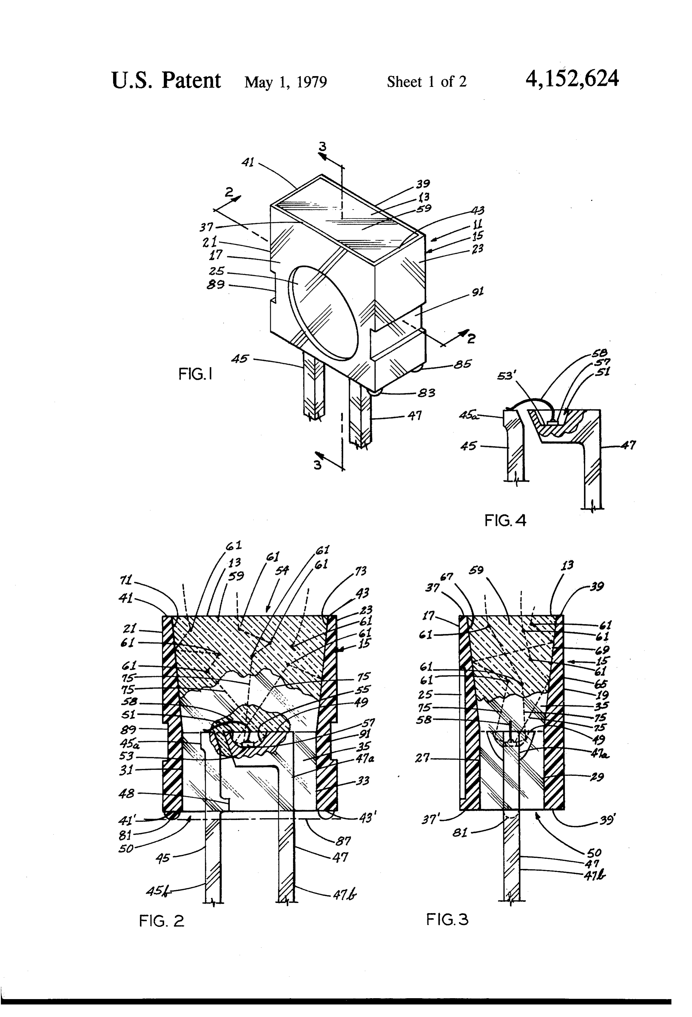
tionship to the electrodes, as by means of a wire bond BRIEF DESCRIPTION OF THE DRAWINGS extending from one of the electrodes to a face surface of the LED body. The lower portions of the electrodes FIG. 1 is a perspective view of an LED device of the extend below the bottom opening of the device to per present invention. . mit connection of a source of electrical power to them 35 FIG. 2 is a vertical cross-section of the device taken for causing the LED to emit light. along line 2-2 of FIG. 1.
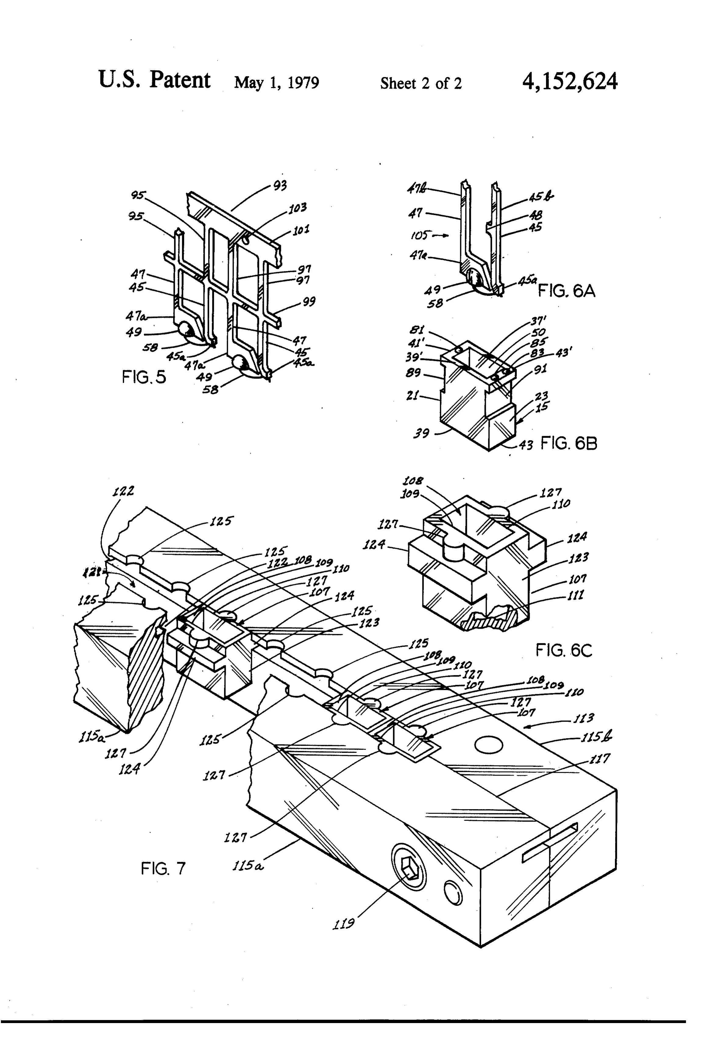
In cross section, the side walls of the housing have a FIG. 3 is another vertical cross-section of the device thickness which increases from thin-walled portions taken along the line 3-3 of FIG. 1. which constitute peripheral upper edges thereof in a FIG. 4 is a side view, partly in cross-section, of a pair direction toward the bottom of the principal cavity to of electrodes having an integral reflective cavity of an define sloped inner walls of the principal cavity which alternate form different from that shown in FIG. 2. slope toward the LED-containing cavity. The principal FIG. 5 is a pictorial view of a section of a lead frame cavity is filled to the upper opening with a light trans and showing two sets of electrode pairs of such lead missive encapsulant of synthetic resin material. Such frame.
encapsulant includes light-scattering particles dispersed 45 FIG. 6A illustrates portions of an electrode pair of therein. The encapsulant surrounds the upper portions such lead frame positioned for insertion into the cavity of the electrodes, the LED-containing cavity, and the of an LED device housing of the present invention in LED. Accordingly, the opening of the principal cavity accordance with a method disclosed herein. provides a light-emitting area of arrayable rectangular FIG. 6B is a pictorial view of such device housing format which emits light of intensity which is substan 50 positioned for insertion into a mold cavity insert. tially uniform across the light emitting area. FIG. 6C is a pictorial view of such mold cavity insert, An economical method of manufacturing such de partly in cross-section, positioned for orientation in a vices comprises forming a conductive lead frame strip mold.
for the LED having a plurality of electrode lead pairs FIG. 7 is a pictorial view, partly in cross-section, connected by at least one integral tie bar extending 55 illustrating such a mold employed in carrying out a lengthwise of the lead frame strip. Each lead pair pro method in accordance with the present description and vides the two electrodes for an LED, as noted above, showing a number of such mold inserts placed in mold with one of each of the electrodes of each pair provid cavity inserts of the mold.
ing a surface area for an LED chip or so-called die. The Corresponding reference characters indicate corre method involves attaching such a die to each surface sponding parts throughout the several views of the area of the lead frame, connecting each die to the re drawing.
spective electrodes of a lead pair. There is then pro DESCRIPTION OF THE PREFERRED vided a mold base having a plurality of adjacent mold cavities spaced along an axis. The spacing between EMBODIMENTS centers of the adjacent mold cavities corresponds to the 65 Referring now to FIG. 1, illustrated generally at 11 is spacing between centers of the adjacent lead pairs. A a new solid state electroluminescent device of the pres mold cavity insert of synthetic resin material is then ent invention. Although device 11 may be arrayed with placed into respective ones of the mold cavities and the similar devices in suitable composite configurations,
Page 6
e.g., to provide a bar-type display or other display con within housing 15 a principal cavity 35 limited by corre figurations, the device may be regarded individually as sponding upper and lower edges of each side wall, such a solid state indicator. being designated 37,37'; 39,39"; 41,41'; and 43,43". Hence Indicator. 11 has a rectangular format light emitting the top of cavity 35 is defined by upper edges 37, 39, 41 area 13 at the top of a housing designated generally 15. and 43, its bottom by lower edges 37, 39, 41' and 43'. Area 13 is nearly as large as the length and width of the The indicator has spaced-apart cathode and anode housing so that substantially the entire top surface of the electrode leads 45 and 47 of electrically conductive device will appear to be illuminated. material such as an alloy of copper, iron, nickel or other Housing 15 is of a molded synthetic resin material metals which may be plated with nickel, gold or other described below of substantially opaque nature, i.e., will 10 metals to prevent oxidation and improve electrical substantially preclude most, if not all, of light emitted contact or facilitate soldering to the electrodes if de within the interior of indicator 11 from being transmit sired. Cathode electrode 45 has a small locking or locat ted through its walls, it being desired that the light ing tab 48 at the level of the housing lower edges. Elec emerge from area 13 rather than "leaking' through the trodes 45 and 47 extend generally vertically through the walls of housing 15. This prevents optical cross-talk 15 bottom opening 50 of cavity 35 and terminate within the between adjacent identical devices when arrayed in cavity at upper ends designated 45a and 47a. The upper contiguous relationship. end 47a of the anode electrode comprises a surface area For reasons more fully explained below, the resin 49 and is generally parallel to and below the top open material of housing 15 is diffusely reflective, at least as ing 54 of cavity 35. Area 49 includes a small integrally to its interior surfaces, so that light falling thereon will 20 formed specularly respective cavity 51 having a bottom be scattered more or less isotropically rather than being surface 53 facing the top opening 54. specularly reflected. Cavity 51 may be of various different configurations. Housing 15 is of a sleeve-like configuration having Preferably it is shown in FIG. 2 as having semihemis four integrally joined side walls, there being a front side pheric interior wall surfaces 55 which merge with bot wall 17, a rear side wall 19, and left and right side walls 25 tom surface 53, the latter being flat. Suitably secured or 21 and 23. Although the outside face of front wall 17 is bonded, as through use of silver epoxy, to the flat bot shown to have a circular indentation or depression 25 molded in it in order to more readily visually orient the tom surface 53 is an LED die 57 of a generally thin flat indicator for correct installation, as well as to provide a be understood,andthetypically configuration rectangular shape. As will pleasing appearance and also to facilitate application of 30 having at least one p-nLED die 57 is a diode structure a logo or other identifying indicia, indentation 25 is provide light emission junction formed therein so as to from electron hole recombina optional. tion at the junction and in space-change regions adja Each of the side walls is preferably rectangular in cent the junction when the junction is forward biased shape. Although it is preferred that the width of each of by a source of power. For such purpose, a thin wire 58, side walls 2 and 23 be less than that of the front wall 17 35 e.g., of gold, is bonded, as by conventional thermocom or rear wall 19, the housing 15 or body of the present pression indicator is rectangular, consistent with the rectangular surface oforcathode ultrasonic welding techniques, to the top light emitting area 13. While the thickness or depth of over the lip of cavityelectrode portion 45a and extends 51 and thence contacts the LED the indicator housing 15 from front to back is a matter die at the bonding point on the die. In this way, the of choice, it has been found that the elongated rectangu 40
LED is series-connected with the electrodes. The light lar light emitting area 13 is commercially desirable and emission more readily facilitates arraying of the indicators in emitting region characteristics and composition of the light contiguous front-to-back relationship, as for assembling of the LED die 57 are discussed below. bar-graph type displays. The lower portions 45b, 47b of the electrodes extend Typically, the dimensions of the present indicator 45 below the bottom opening of cavity 35 as leads for permitting connection of a suitable source of electrical may be quite small. For example, the light emitting area may be about one-quarter inch (6.4 mm) in width and power, such as a d.c. current source, to cause recombi about one-eighth inch (3.8 mm) in depth, i.e., from front nant emission of light from the LED die 57. to rear. The height of each of the side walls may typi The LED die is surrounded by a light-transmissiye cally be about a little more than one-quarter inch (6.8 encapsulant 59 of synthetic resin material which fills mm). Consequently, a typical device of the present cavity 35.
invention is highly miniaturized, although larger sizes The manner in which rays of light emanating from are quite feasible. LED die 57 are directed toward the top opening so as to In the preferred rectangular configuration, arraying illuminate area 13 is a matter of considerable signifi or so-called stacking of the devices in multiple configu 55 cance determined not only by the emission characteris rations is possible. To facilitate molding of the housing, tics of the LED die, the shape and reflective character it may have a very slight tapering inward from bottom istics of the LED-containing cavity 51, and geometric to top, but area 13 and its walls remain rectangular to configuration and reflective characteristic of the inte permit arraying. Multiple configurations may be either rior surfaces of side walls 17, 19, 21 and 23, but also by in front-to-back relationship or in side-by-side configu encapsulant 59. These several considerations, while ration. Hence, there may be either "x-axis' or "y-axis' necessarily coacting and providing the desired synergis arraying, or both, of the present solid state indicator, tic result for uniformly illuminating area 13 with bright permitting large composite light emitting areas to be light are discussed individually in detail. assembled. It will be understood that since encapsulant 59 en Referring to FIGS. 2 and 3, wherein the new solid 65 tirely fills principal cavity 35, it entirely surrounds the state indicator is shown in cross-section, the side walls LED structure and fills the LED-containing cavity 51. 17, 19, 21 and 23 and corresponding interior surfaces 27, Preferably, but not necessarily, encapsulant 59 is pig 29, 31 and 33, have inwardly sloping portions to provide mented by incorporation of a dye. For example, if the
Page 7
LED is red light-emitting, then the encapsulant may the die are reflected off the sides of the LED-containing include a red dye. a . . cavity 51 and thence upward where they may strike one The encapsulant has a light-scattering characteristic, of the light scattering centers 61 or one of the interior constituted by light-scattering centers 61 dispersed. surfaces 67, 69, 71 and 73. Alternatively, an LED of throughout the encapsulant. Preferably, encapsulant 59 5 GaAsP having a Lambertian emission characteristic is a two-part epoxy resin constituted by a resin and a may be employed. Thus, while some rays of light ema hardener, such as a cyclo-aliphatic diepoxide resin and nating from a GaAsP die may strike the sides of cavity suitable curing agent therefore. Broadly, approximately 51, the majority of the flux is upward and strikes the from 5 to 100% by weight of borosilicate glass in the light scattering centers on interior surfaces before form of particles or beads is dispersed in the encapsu O emerging from area 13.
lant, but preferably the borosilicate glass constitutes In this regard, it is important to recognize that both from about 20% to about 50% by weight of the encap isotropic and Lambertian emitters may be employed in sulant. commercial LED devices. Thus, the active region of a In a commercially preferred embodiment the borosili red light emitting LED is usually of GaAsP, although cate glass is approximately 325 mesh and constitutes 15 the substrate thereof may be of Gap, GaAs, GaAsP or about 33% (about one-third) by weight of the encapsu even Ge, but has in any event a Lambertian emission lant. characteristic. Toward the other end of the visible spec Considering now the housing 15, it is preferred to trum, e.g., for green light emission, it is usual practice to employ a premolded plastic material of a resilient or employ an LED in which the active region is of GaP, semi-resilient nature. Although it is commercially pre 20 and accordingly having an isotropic emission character ferred to use a polycarbonate which can be injection istic. The present indicator device may advantageously molded, the housing may instead be of injection molded accommodate either type of emitter and thus can be thermoplastics such as polystyrene, polyethylene, poly commercially produced for emission of light of any propylene, nylon, polychlorotrifluorethylene, polytet desired color capable of being generated by an LED. rafluorethylene and ABS or may be molded in other 25 In FIGS. 2 and 3, various rays of light are shown manners using various thermosetting plastics consti emanating from the LED die to illustrate these various tuted of suitable synthetic resin materials. When poly characteristics. Thus, a ray such as designated 75 may carbonate is employed, it is preferred to impart white strike scattering centers 61 before emerging from area pigmentation thereof by incorporation of broadly about 13, while another ray such as shown at 77 may strike 8 to 12% by weight of TiO2 preferably about 10 to 12%. 30 some of the light scattering centers 61 and thence be Accordingly, a diffusively reflective and commercially diffusively reflected (as indicated at 79) off an interior attractive finish results. Accordingly, reflection off the surface of a housing wall, and thence emerge or strike interior surfaces of the housing walls is approximately other scattering centers. The result is uniform emission isotropic in nature. of light from area 13 so that it appears to be uniformly Those portions of the sidewalls of the housing adja 35 illuminated without any unevenness or "hot spot' at its cent the top opening of cavity such as shown at 63 in the center.
front view cross-section and at 65 in the side view cross In order to more readily identify which of electrode section are desirably quite thin so that only a very thin leads 45 and 47 is the cathode and which is the anode, lip or margin of the housing, constituted by upper edges integrally molded along lower housing edges 41' and 43' 37, 39, 41 and 43 is apparent when the device is viewed are rounded protrusions or "stand-offs' 81, 83 and 85. from above. Protrusion 81 is centered along lower edge 41' and Referring again to FIGS. 2 and 3, the interior sur adjacent cathode electrode 45. Protrusions 83,85 are faces 27, 29, 31 and 33 of the side walls have flat faced spaced apart along lower edge 43' at the opposite side of portions correspondingly designated 67, 69, 71 and 73 the device and are adjacent anode electrode 47. These which slope inwardly from the respective upper edges 45 protrusions all extend downward the same distance 37, 39, 41 and 43 toward the LEED-containing cavity 51. from the housing lower edge. Since there are three such Thus, the walls in cross-section are tapered and increase protrusions spaced as shown, they provide an inher in thickness from thin upper edges to a constant thick ently stable spacing of the device from the surface of a ness at a point proximate the level of electrode surface printed circuit board 87 (FIG. 2) when mounted area 49. The housing, as a consequence, is not only 50 thereon, as is typically desirable for devices of such sufficiently strong to maintain structural integrity and character and other circuit elements so mounted. to resist deformation or the like both before and after The new device may be mounted in other ways, for manufacturing a completed indicator, but also provides example, the upper portion may be positioned so as to the desired optical qualities. extend through or be abutted against an aperture in an Although, as noted, the LED-containing cavity 51 is 55 equipment panel, fascia, or the like so that the illumi shown with semihemispheric interior side walls, the nated area 13 is visible from the front. For facilitating cavity may be formed as shown in FIG. 4 wherein the such installations, the housing 15 is formed with shallow cavity, designated 51", has side walls 55' which form an channels 89 and 91 extending laterally across the width angle with the floor 53 of the cavity, the LED die 57 of the side walls 21 and 23, respectively. Such channels being secured as previously described. It is also envi are useful for receiving a retainer clip (not shown) or sioned that a two-piece cavity for the LED die may be other means for retaining the device in predetermined employed rather than one formed entirely in the surface position for use as an indicator. of only one electrode. Thus, part of the cavity may be in Referring to FIG. 5, devices of the present invention one electrode, another part in the other electrode. are manufactured by a method beginning with the for The new solid indicator device may utilize both iso 65 mation of a conductive lead frame 93 of plated alloy tropic and Lambertian emitters. Thus, a GaP LED composition as described above. Such lead frame (only having a generally isotropic emission characteristic may a portion of which is shown) has electrode lead pairs be utilized, since light rays emanating from the sides of 95.97 secured together by an integral tie bar 99 extend
Page 8
ing lengthwise of the lead frame across intermediate While various such materials may be employed, each portions of the leads and a parallel mounting portion or such insert is of premolded configuration, its cavity 108 main tie bar 101 of greater width than bar 99 and having being dimensioned for receiving an indicator device one or more locating holes 103. Tie bar 99 may be housing 15 of predetermined shape and size. In this sheared so as to leave only the locating tab 48secured to regard, it will be understood that while the dimensions each cathode lead. Such shearing operation may, but of cavity 108 may be varied for receiving different sizes not necessarily, also sever either the cathode or anode of device housings 15, the exterior dimensions of the of each lead pair from main tie bar 101 so that the LED mold inserts 107 remain the same so as to permit use of die which is attached in the integral reflective cavity of the same mold 113 for a class of different sizes of indica each anode electrode may be tested without the leads 10 tor devices.
being shorted by either of the bars 99 and 101. How Several inserts 107 are shown in position between the ever, such electrode shearing and testing may be de halves 115a, 116b of mold 113. After the inserts (e.g., ferred until after the assembly of completed devices, ten in number) are so placed and secured in the mold, a The specific configuration of tie bars is chosen to device housing 15 is thereafter placed in each insert facilitate automated processing of lead frames in which 15 cavity 108, the floor 111 of each insert 107 then defining the LED dies are inserted and bonded to such integral a closure of the principal cavity 35 of each device hous reflective cavities, the lead wires 58 suitably secured, ing. A lead frame consisting of electrode assemblies 105 and appropriate portions of tie bar 99 sheared. is then suitably positioned above the corresponding FIG. 6A shows an assembled electrode lead pair device housings as by means of a clamp or the like. assembly 105 including an LED device or die series 20 Mold 113 is preferably then heated to a temperature connected with the electrodes 45 and 47 by means of suitable for causing even flow of the encapsulant char wire 58. As will be understood, a plurality of such as acterized above, such temperature being referred to as semblies 105 remain secured to main tie bar 101. an encapsulation temperature and preferably approxi In accordance with the presently described novel mately 90' to 100 C. In this regard, the material of method of economically manufacturing the solid state 25 which the mold inserts 107 are formed must be capable indicators, devices are formed as an ingegral unit by of withstanding this temperature through repeated inserting an LED-and-electrode assembly 105 within molding operations, it being desirable to reuse the in the cavity 50 of a device housing 15 oriented as shown serts many times. An ABS material is useful for these in FIG. 6B, and by introducing the encapsulant 59 and purposes, retaining dimension well to continuous tem curing it until it solidifies. 30 peratures of more than 150° C. Other thermoplastics For this purpose, it is preferred to utilize a mold in may be used.
which are inserted a plurality of mold inserts 107 each The steps are then carried out of moving the lead of a configuration shown in FIG. 6C. Each insert 107 frame 93 relative to mold 113 to position the surface has a cavity 108 having an opening 109 for receiving the area 49 of the electrode pair (having an LED positioned device housing 15. The dimensions of the insert cavity 35 in its cavity 51) within the cavity 50 of each device 109 are preselected by providing spacing between walls housing 15 to an extent shown in FIGS. 2 and 3. The thereof (such as that designated 110) to closely accom location tabs 48 facilitate such positioning. modate and thus telescopically receive the device hous Either before or after such positioning of the elec ing. Such mold insert 107 has a floor 111 against which trode assemblies the encapsulant is then introduced by the housing's upper walls edges 37, 39, 41 and 43 abut suitable means (such as syringes or pipettes from a com when the housing is placed within cavity 108 when the mon source) into each device cavity 50 in an amount housing is oriented in the inverted position shown in sufficient to cause encapsulation of the LED die posi F.G. 6B. tioned therein, and preferably to fill entirely each cavity A two-piece mold 113 for carrying out the method is 50. It will be apparent that the floor 111 of insert 107 shown in FIG. 7 and includes halves 115a, 11.5b which 45 retains the encapsulant and thus serves to delineate the are adapted to be fitted together in mating relationship light-emitting or so-called illuminated area 13 of a de as shown at 117 and secured as by means of screws, such vice after the encapsulant hardens. as shown at 119, which extend through a bore in mold Following encapsulation, the relationship of elements half 115a and threaded into mold half 115b, thereby is maintained for a cure period, while the mold is raised permitting the two halves to be readily disassembled. 50 to a cure temperature of about 120-140 C. and the Extending lengthwise of the mold is a longitudinal encapsulant permitted to cure for at least about one cavity or spacing 121 of cruciform cross-section having hour.
lengthwise channels 122 in each mold half, such cross At the end of the cure period, the encapsulant is section being illustrated by the corresponding cross-sec sufficiently hardened that the lead frame and mold may tion of an end face 123 of mold cavity insert 107, the 55 be moved relatively away from each other, thereby latter having flanges 124 for fitting within channels 122. withdrawing prefinished LED indicator devices 11 Preferably spaced at intervals along cavity 121 of the from the mold inserts. A post curing procedure is then mold are notches 125 for accommodating correspond desirably carried out by subjecting the prefinished de ing projections 127 of mold insert 107, so as to secure vices to a post cure temperature of about 120-140 C. the latter in place longitudinally with mold 113 in longi 60 for several hours to cause complete curing of the encap tudinally aligned relationship with the spacing between sulant, and the relieving of stresses and the like for high adjacent centers of the mold inserts 107 and housings 15 device reliability.
positioned therein corresponding relatively precisely to Finally, shearing or trimming of the main tie bar 101 centers between adjacent pairs of electrode pair assem from at least one electrode is carried out (if not previ blies 105 of the lead frame. 65 ously effected) and the finished devices are tested for The mold is preferably of a suitable thermally con proper operation and brightness. The finished devices ductive, long-lasting material such as steel. The mold are then sheared totally from the tie bar 101 and suitably cavity inserts 107 are of a synthetic resin material.. prepared for packaging.
Page 9
As various changes could be made in the above meth 8. A device as set forth in claim 7 wherein said LED ods and products without departing from the scope of comprises GaAsP.
the invention, it is intended that all matter contained in 9. A solid state electroluminescent device having a the foregoing description or shown in the accompany light-emitting top area of rectangular format which is ing drawings shall be interpreted as illustrative rather 5 suited for being arrayed with other such devices in than in a limiting sense. contiguous relationship without optical cross-talk there The specific embodiments described or shown herein between, the device comprising a housing of molded are intended to be illustrative, the scope of the invention synthetic resin material which is substantially opaque being indicated by the following claims wherein all 10 and which is diffusely reflective, the housing having variations within the range of equivalence are intended four integrally joined side walls defining a generally to be encompassed. rectangular body for the device, each of the side walls What is claimed is: having exterior surfaces of generally rectangular shape, 1. A solid state electroluminescent device comprising the interior surfaces of the side walls having peripheral a housing of molded synthetic resin material which is 15 upper and lower edges defining a principal cavity hav substantially opaque and which is diffusely reflective, ing a top and a bottom, the top being an opening of the housing comprising integrally joined side walls rectangular shape, a pair of spaced electrodes of electri defining a body for the device, said side walls having cally conductive material extending generally vertically interior surfaces having peripheral upper and lower through the bottom, the electrodes each having upper edges defining a principal cavity having a top and a portions extending from the bottom into the principal bottom, the top constituting a light-emitting opening of 20 cavity and terminating within the cavity at upper ends, predetermined shape, a pair of spaced electrodes of the upper ends of the electrodes providing a surface electrically conductive material extending generally area in at least one of the electrodes which is generally vertically through the bottom, the electrodes each hav parallel to and below the top opening and which is ing upper portions extending from the bottom into the 25 positioned within the cavity, the surface area including principal cavity and terminating within the cavity at an integral specularly reflective LED-containing cavity upper ends, the upper ends of the electrodes presenting formed by the material of the electrodes, the LED-con an area in at least one of the electrodes below the top taining cavity having a bottom surface facing said top opening and positioned within the cavity, said area opening, an LED having a body of semiconductor ma including an integral specularly reflective LED-con 30 terial, the LED body being positioned within the LED taining cavity having a bottom surface facing said top containing cavity, means for interconnecting the LED opening, an LED having a body of semiconductor ma body in series-connected electrical circuit relationship terial, the LED body being positioned within the LED with the electrodes, the lower portions of the electrodes containing cavity, means for interconnecting the LED extending below the bottom opening to permit connec body in series-connected electrical circuit relationship 35 tion to a source of electrical power to the electrodes for with the electrodes, the lower portions of the electrodes causing the LED to emit light, the side walls of the extending below the bottom opening to permit connec housing having in cross section a thickness which in tion of a source of electrical power to the electrodes for creases from peripheral upper edges of the side walls in causing the LED to emit light, the housing side walls a direction toward the bottom of the principal cavity to having inner surfaces which slope toward the LED define sloped inner walls of the principal cavity which containing cavity, the principal cavity being filled with slope a light transmissive encapsulant of synthetic resin mate cavitytowardbeing the LED-containing cavity, the principal filled to the top with a light transmissive rial having a light-scattering characteristic, the encapsu encapsulant of synthetic lant surrounding said upper portions of the electrodes, including light-scatteringresin material, the encapsulant particles dispersed therein, the LED-containing cavity, and the LED, whereby 45 the encapsulant surrounding said upper said light-emitting opening emits light of substantially electrodes, the LED-containing cavity, portions and the of the
LED, uniform intensity thereacross.
2. A device as set forth in claim 1 wherein the periph light-emitting area of arrayable rectangular formata whereby the opening of the principal cavity provides eral upper edges of the side walls of said housing are which emits light of intensity which is substantially constituted by a thin region of said side walls to provide 50 uniform across the light-emitting area. , said light-emitting with dimensions which are nearly as great as corresponding dimensions of the housing when tom10.ofAsaid device as set forth in claim 9 wherein the bot principal cavity defined by the side walls of viewed from above the device.
said housing is constituted by a bottom opening of rect 3. A device as set forth in claim 2 wherein said light angular emitting opening is of rectangular shape. 55 shape, the electrodes extending through the 4. A device as set forth in claim 1 wherein the elec bottom opening.
trodes are constituted by a spaced lead pair formed 11. A device as set forth in claim 9 wherein said light from a metal lead frame strip. scattering characteristic is constituted by light-scatter 5. A device as set forth in claim 1 wherein said LED ing centers dispersed in said encapsulant. comprises a monocrystalline semiconductor material 12. A device as set forth in claim 9 wherein said en having a substantial isotropic light emission characteris capsulant comprises a transparent epoxy resin, said tic light-scattering centers comprising borosilicate glass. 6. A device as set forth in claim 5 wherein said LED 13. A device as set forth in claim 12, said LED emit comprises GaP. ting red light, said encapsulant including a red dye, said 7. A device as set forth in claim 1 wherein said LED 65 borosilicate glass constituting from about 20% to about comprises monocrystalline semiconductor material 50% by weight of said encapsulant. having a substantially Lambertian light emitting charac 14. A device as set forth in claim 13, said LED com teristic. prising GaAsP.
Page 10
15. A device as set forth in claim 13 wherein said device from a printed circuit board or the like when a borosilicate glass is approximately 325 mesh and consti device is mounted thereon.
tutes about 33% by weight of said encapsulant. 19. A device as set forth in claim 9 wherein there are 16. A device as set forth in claim 11 wherein said two of said protrusions adjacent one of the electrodes housing comprises a diffusely reflecting material. and one of said protrusions adjacent the other electrode, 17. A device as set forth in claim 11 wherein said said three protrusions each extending downward from diffusely reflecting material comprises a polycarbonate said lower edge of the housing by the same distance to plastic having about 8 to 12% by weight of TiO2 provide an inherently stable spacing of said device from therein. a printed circuit board or the like when mounted 18. A device as set forth in claim 9 wherein one of 10 thereon.
said electrodes is a cathode lead for the LED and the 20. A device as set forth in claim 9 wherein two of the other of said electrodes is an anode lead for the LED, side walls of said housing which are opposite from each the peripheral lower edge of said housing having one or other each have a channel formed in the exterior surface more protrusions integrally formed thereon adjacent thereof, said channel extending across the width of said one of said electrodes, such protrusion extending down 15 housing, said channel being useful for receiving means ward from said lower edge and signifying which of said for retaining said device in a predetermined position for electrodes is the anode lead and which of the electrodes use as an indicator.
is the cathode lead, such protrusion also spacing said
Provenance
- Collection
- Cited prior art
- Original PDF
- patentimages.storage.googleapis.com →
- Filed
- 1978-03-16
- Pages
- 10
- Method
- pdftotext (the PDF's own text layer) + pdftoppm 300dpi page scans
- Source
- Google Patents bibliographic record
- Granted
- 1979-05-01
- Inventors
- Vincent J. Knaebel; Monsanto Co
- Transcribed from
- patentimages.storage.googleapis.com →