patent · US4074101
Induction heating apparatus using a pair of inversely parallel connected gate-controlled switching devices
14 February 1978
Page 1 — bibliographic record
United States Patent (19) 11) 4,074,101 Kiuchi et al. (45) Feb. 14, 1978 54) INDUCTION HEATINGAPPARATUS USING 3,693,069 9/1972 Kelley et al. .............. 219/10.77 UX A PAR OF INVERSELY PARALLEL 3,707,667 12/1972 Gyugyi .............................; 321/69 R CONNECTED GATE-CONTROLLED 3,735,237 5/1973 Derby...... ... 219/10.55 B SWITCHING DEVICES 3,743,919 7/1973 Bingley .............................. 321/69 R 3,747,301 7/1973 Glover et al. ...... ... 55/DIG. 36 75) Inventors: Mitsuyuki Kiuchi; Keizo Amagami; 3,821,509 6/1974 Amagami et al. ................ 219/10.77 Takumi Mizukawa; Hideyuki 3,898,410 8/1975 Peters ................................ 219/10.49 Kominami, all of Kadoma, Japan 3,925,633 12/1975 Partridge..... ... 219/10.77 4,002,875 1/1977 Kiuchi et al. ..................... 219/10.77 73) Assignee: Matsushita Electric Industrial Co.,
Ltd., Japan Primary Examiner-Bruce A. Reynolds
Attorney, Agent, or Firm-Robert E. Burns; Emmanuel (21) Appl. No.: 657,307 J. Lobato; Bruce L. Adams (22 Filed: Feb. 11, 1976 57) ABSTRACT (30) Foreign Application Priority Data An induction heating apparatus comprising a pair of Feb. 14, 1975 Japan .................................. 50-19251 inversely parallel-connected gate-controlled switching devices connected to an alternating current source, a 51) Int. Cl. ............................................... H05B 5/04 resonant circuit including an induction heating coil and 52 U.S. Cl. ...................... 219/10.49 R; 55/DIG. 36; a variable frequency gating circuit for firing the switch 219/10.55 B; 219/10.77; 307/252 Q; 323/24; ing devices to generate oscillations through the con
58) Field of Search ............... 219/10.49, 10.77, 10.81, ducting device and the induction heating coil. The 219/10.55R, 10.55 E, 10.55 F, 10.55 D; 321/69 switching devices are gated into conduction in succes R, 45, 14, 6; 323/24, 34, 25; 55/DIG. 36, 101; sion in a first order during the positive half cycle of the 126/299 B; 98/115 K, 115 R; 307/252T, 252 alternating current and in a reversed order during the UA, 252 Q, 252 N; 363/160 negative half cycle. A zero crosspoint detector is pro
vided to inhibit gating when the source voltage is near zero crosspoint level and to control the gating fre
3,088,453 5/1963 Grahn et al. ................. 219/10,55 D the source voltage to increase the turn-off time of the 3,268,794 8/1966 Tanaka ................................... 321/66 switching devices for lower input source voltage. 3,538,417 11/1970 Nijhof et al. ......................... 363/160 3,587,555 6/1971 Cerola ........................... 219/400 UX 23 Claims, 26 Drawing Figures
Page 2
Drawing sheet — no readable text.
Page 3
Drawing sheet — no readable text.
Page 4
Drawing sheet — no readable text.
Page 5
Drawing sheet — no readable text.
Page 6
Drawing sheet — no readable text.
Page 7
Drawing sheet — no readable text.
Page 8
Drawing sheet — no readable text.
Page 9
Drawing sheet — no readable text.
Page 10
Drawing sheet — no readable text.
Page 11
Drawing sheet — no readable text.
Page 12
Drawing sheet — no readable text.
Page 13
Drawing sheet — no readable text.
Page 14
nected SCR--s is shown connected in parallel to a reso
INDUCTION HEATING APPARATUS USING A nant circuit;
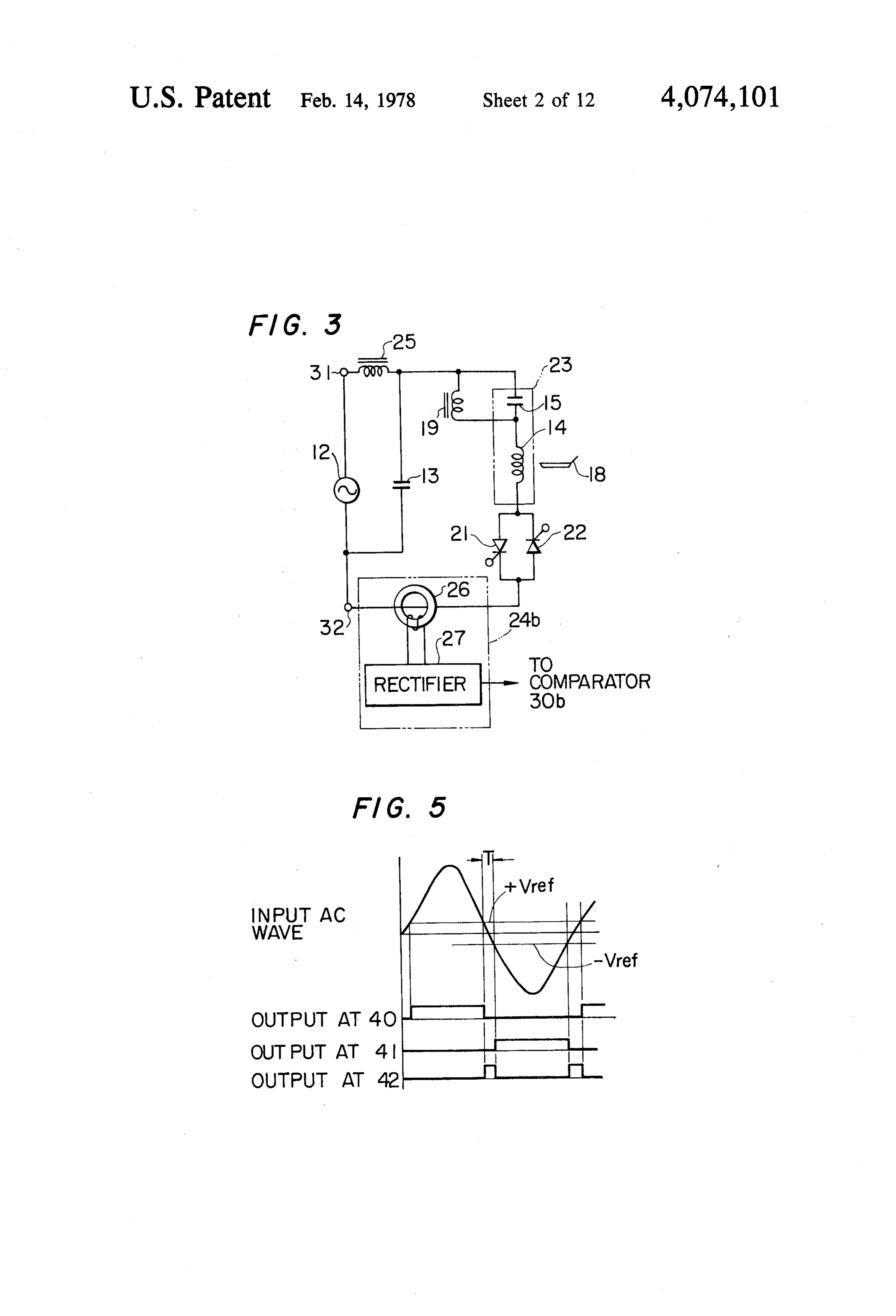
PAR OF INVERSELY PARALLEL CONNECTED FIG. 3 is a circuit diagram of another embodiment of GATE-CONTROLLED SWITCHING DEVICES the invention in which the SCR pair is connected in BACKGROUND OF THE INVENTION 5 series circuit relation to the resonant circuit; FIG. 4 is a circuit diagram of a firing circuit of the
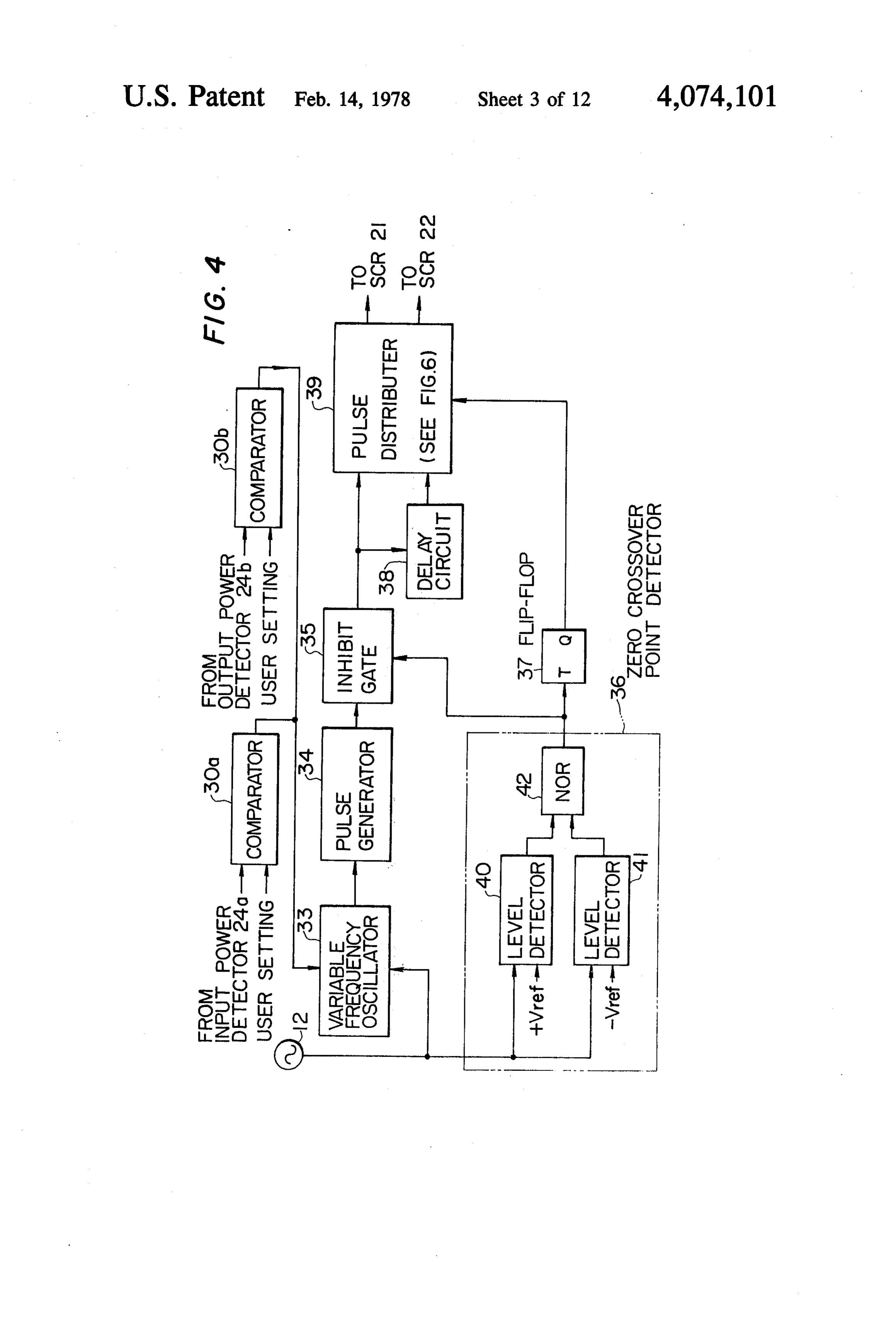
The present invention relates generally to induction invention used in connection with the circuits of FIGS. heating and particularly to an induction heating appara 2 and 3;
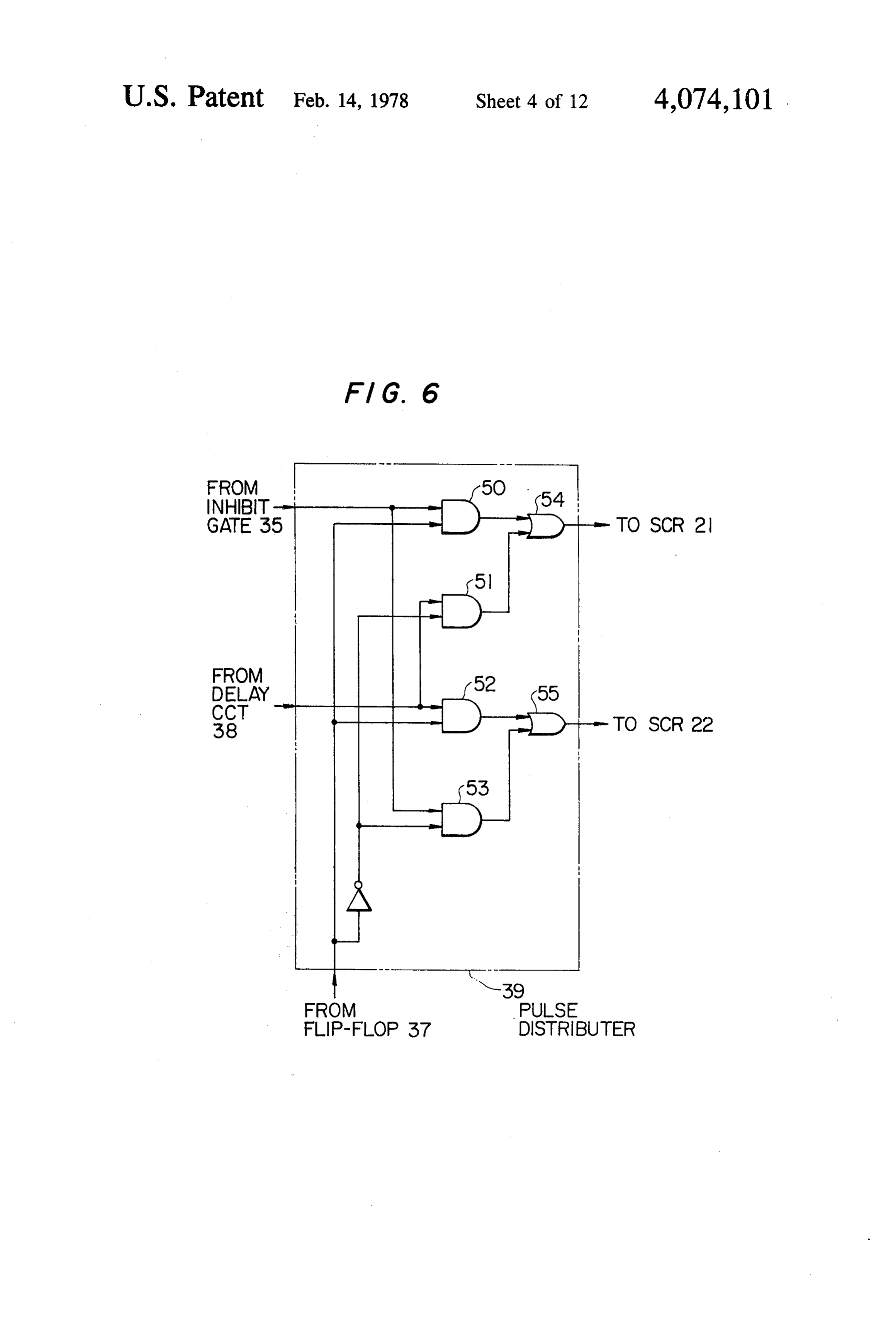
tus which comprises a cycloconverter including a pair FIG. 5 is a graph showing a series of waveforms of inversely parallel connected gate-controlled switch 10 appearing in a zero crosspoint detector of FIG. 4; ing devices. FIG. 6 is a detailed circuit of a pulse distributor of In U.S. Pat. No. 3,821,509 issued to the same assignee FIG. 4;
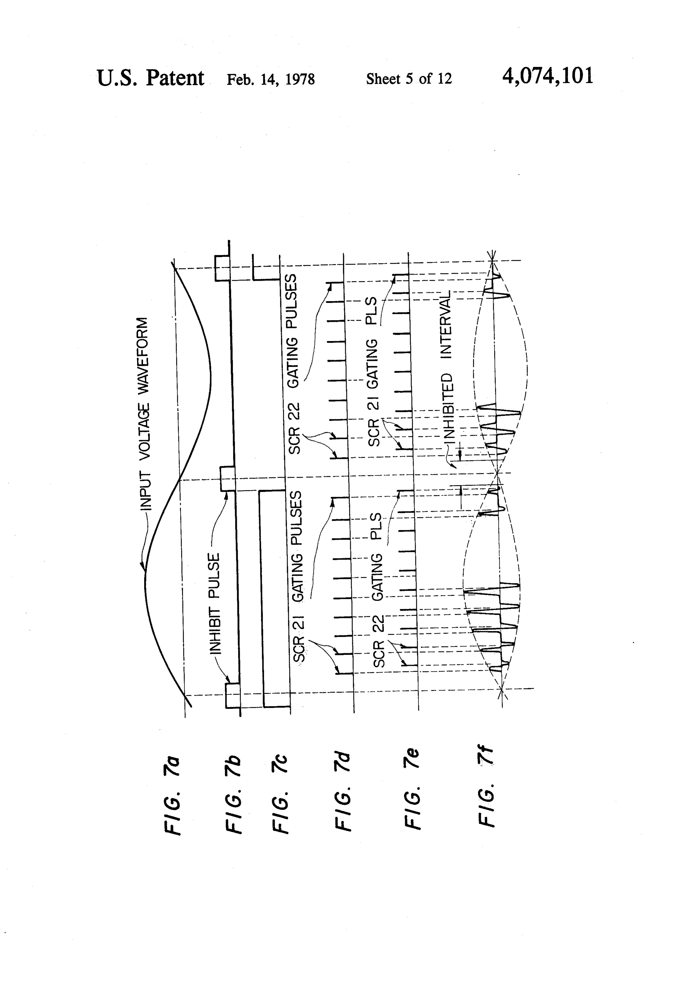
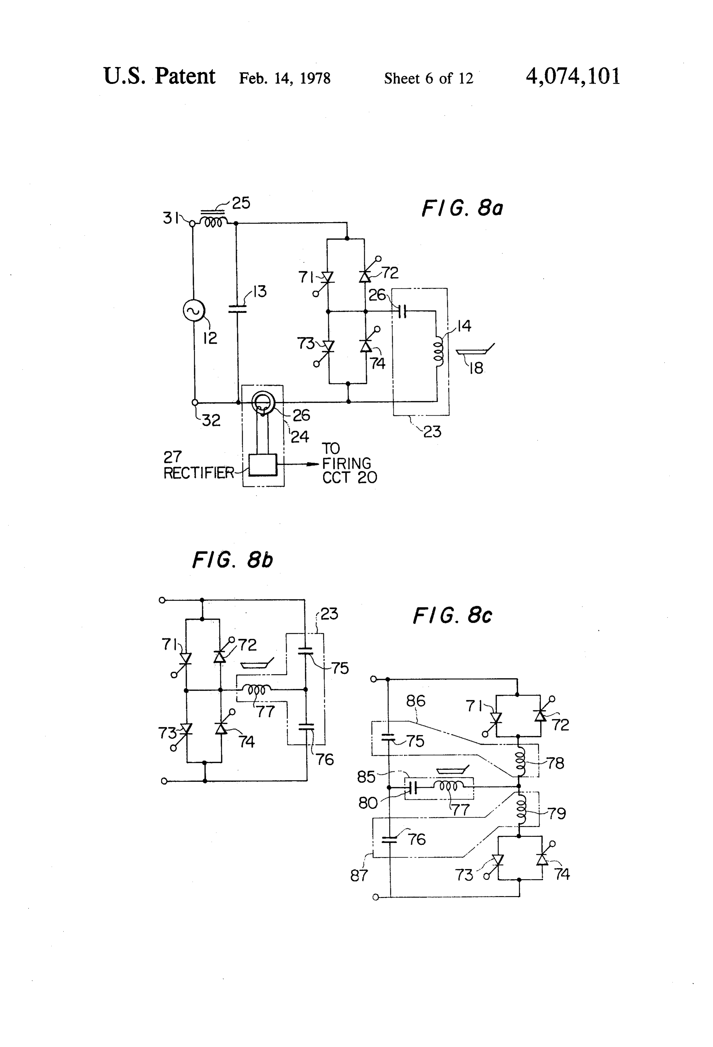
as the present invention, there is described a solid state FIG. 7(a-f) is a waveform diagram useful for explain power converter which includes a gate controlled uni 15 ing the operation of the circuit of FIGS. 2 to 4; directional switching device and a feedback diode in FIGS. 8a to 8c are circuit diagrams of another em versely parallel connected to the switching device, and bodiment of the invention in which two pairs of in a resonant or commutating circuit connected in parallel versely parallel connected solid state switching devices with the switching device. The resonant circuit includes are employed in different circuit relations with resonant an induction heating coil and a capacitor which are circuits;
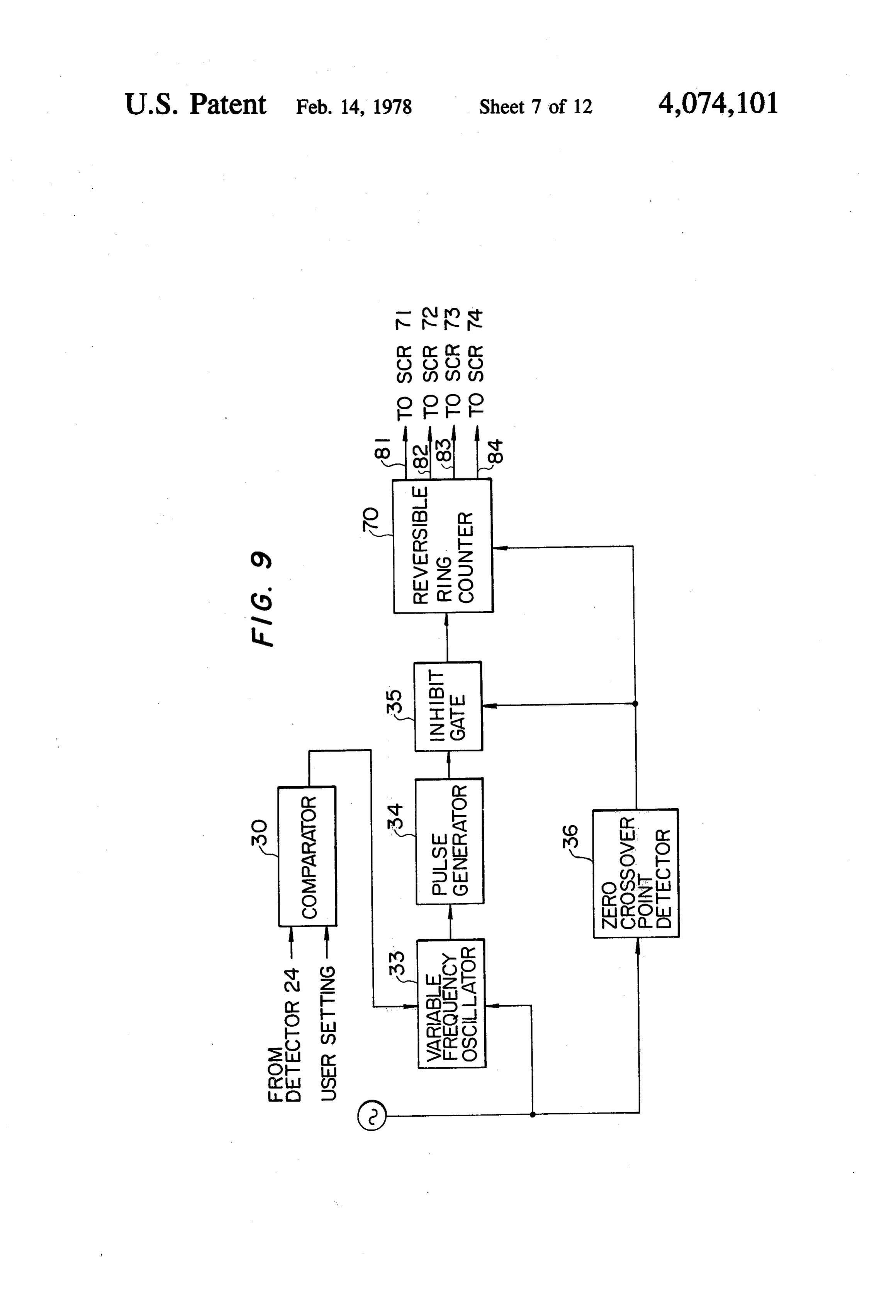
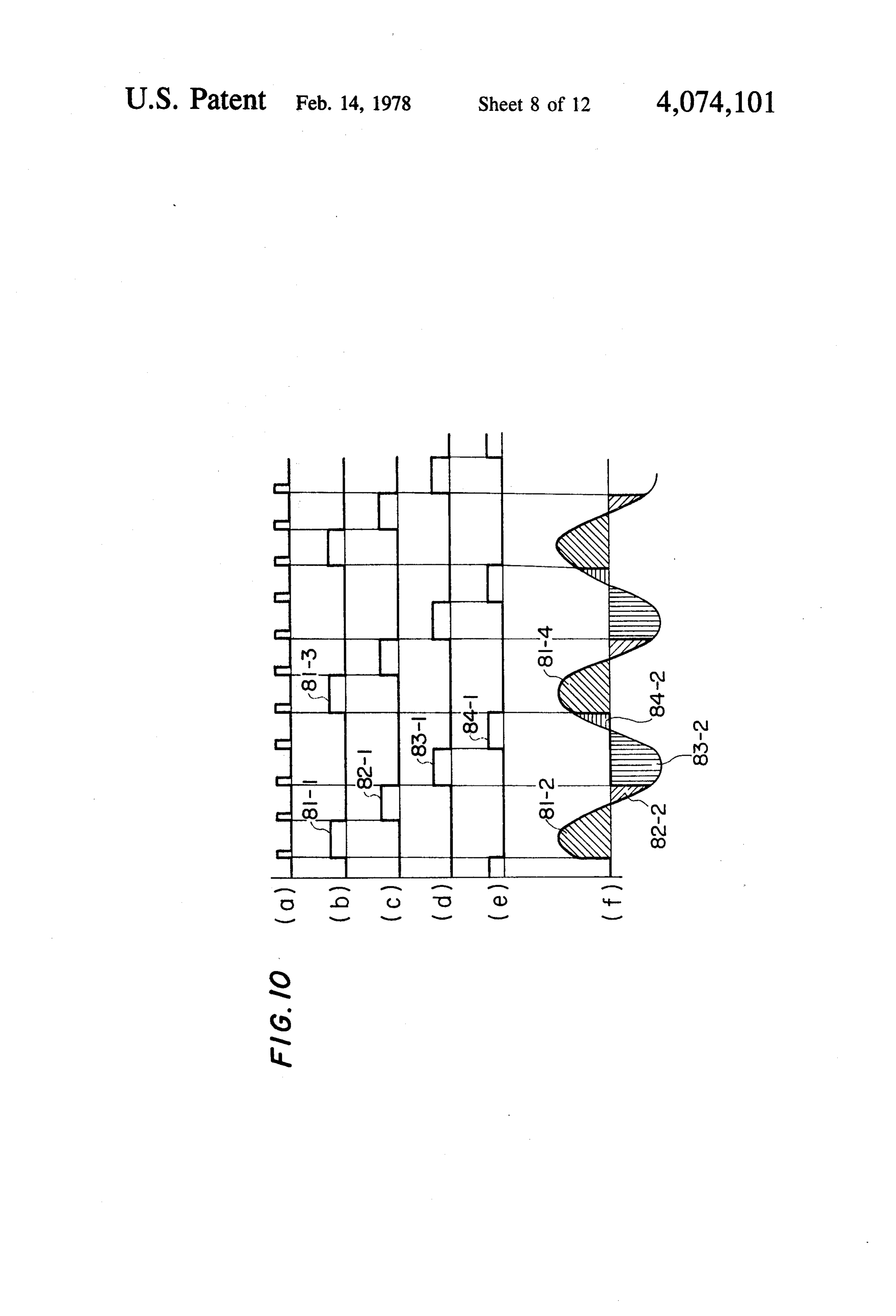
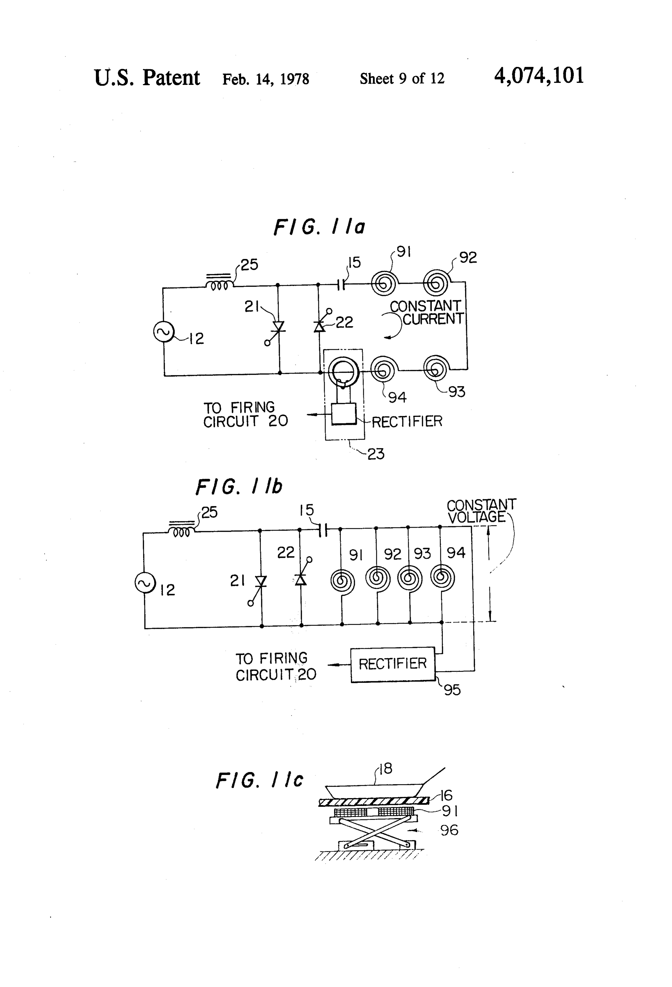
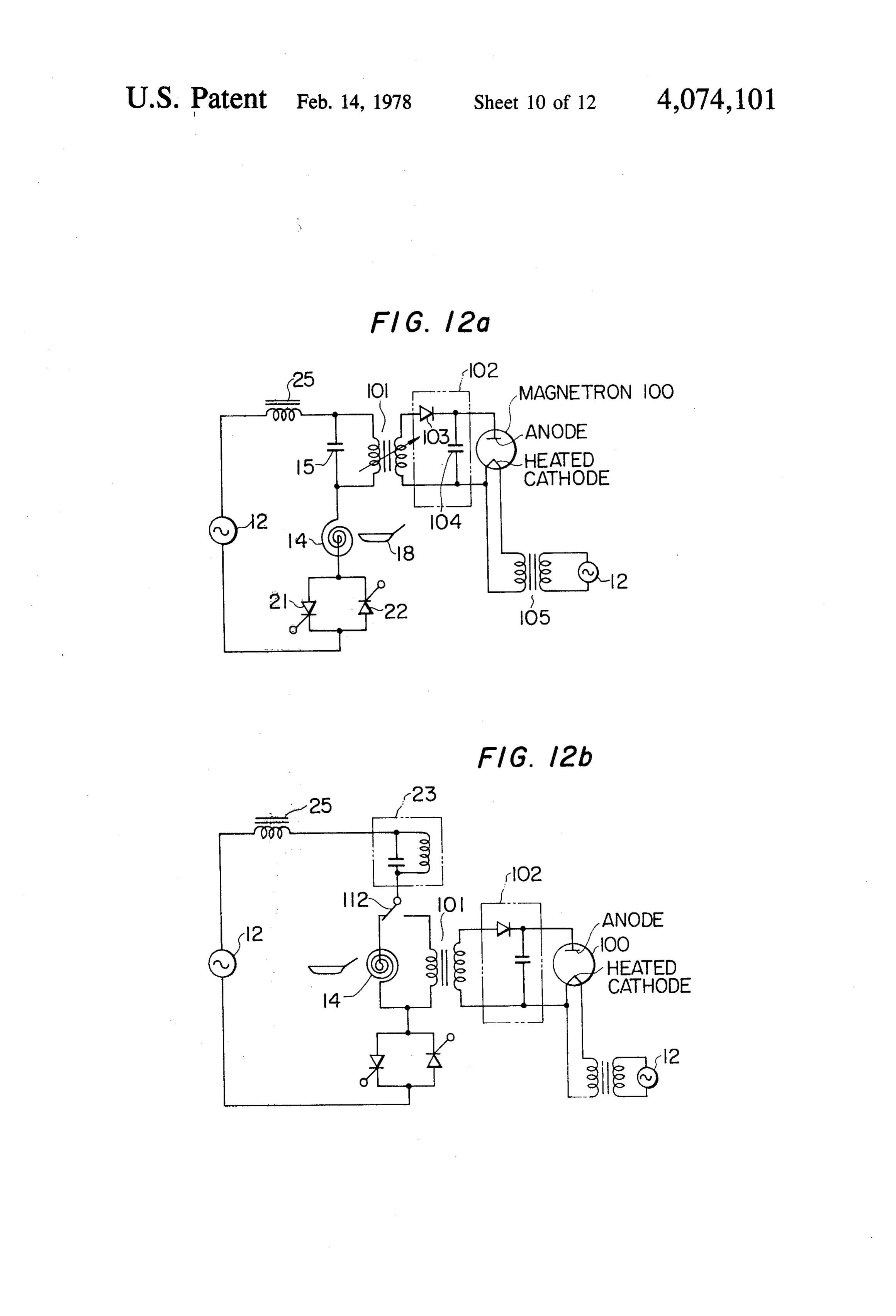
tuned to a high frequency of the order of 20 kHz. A 20 FIG. 9 is a diagram of a firing circuit used in connec full-wave rectifier supplies rectified, unfiltered unidirec tion with the circuits of FIGS. 8a to 8c, tional voltage to the power converter. A gating circuit FIG. 10 is a waveform diagram useful for describing is provided to drive the switching device directly from the operation of the circuit of FIGS. 8 and 9; the rectified unidirectional voltage. Upon gating of the FIGS. 11a and 11b illustrate methods of controlling switching device, the charge stored on the capacitor 25 theFIGS. output of the cycloconverter of the invention; 12a and 12b illustrate another embodiment of will be oscillated through the gated switching device the invention in which the power output from the cy and through the induction heating coil to reversely cloconverter charge the capacitor. Upon reversal of the polarity, the unidirectional isvoltage utilized in delivering a high tension for powering a magnetron used switching device is turned off and a reverse current will 30 in a microwave oven;
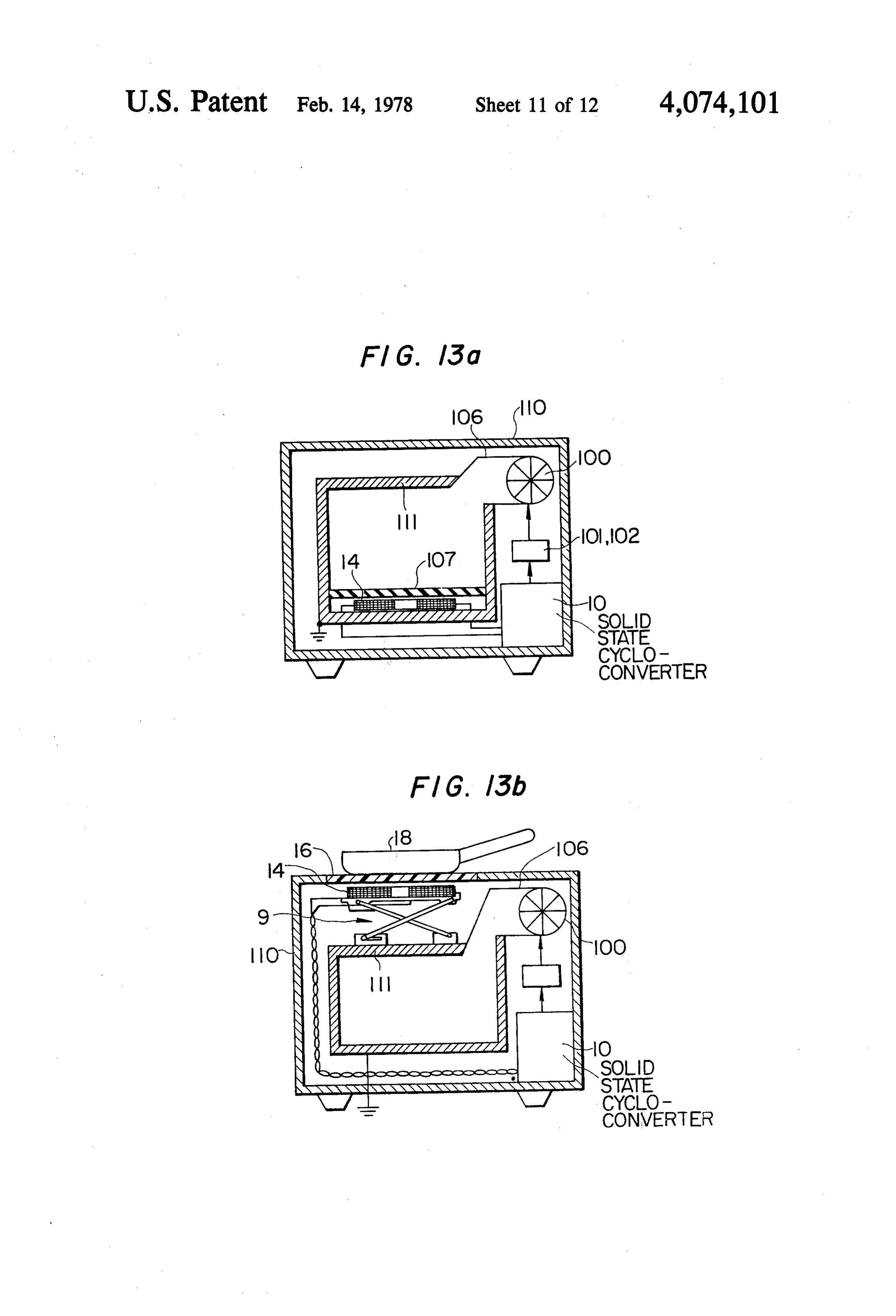
flow through the feedback diode and through the in duction heating coil to return the capacitor to the origi theFIGS. 13a and 13b are schematic views illustrating arrangement of various components of the embodi nal charge minus any losses due to loading.
However, a comparatively greater number of compo ment of FIGS. 12a and 12b nents used in the known power converter with the 35 ment of14theis invention
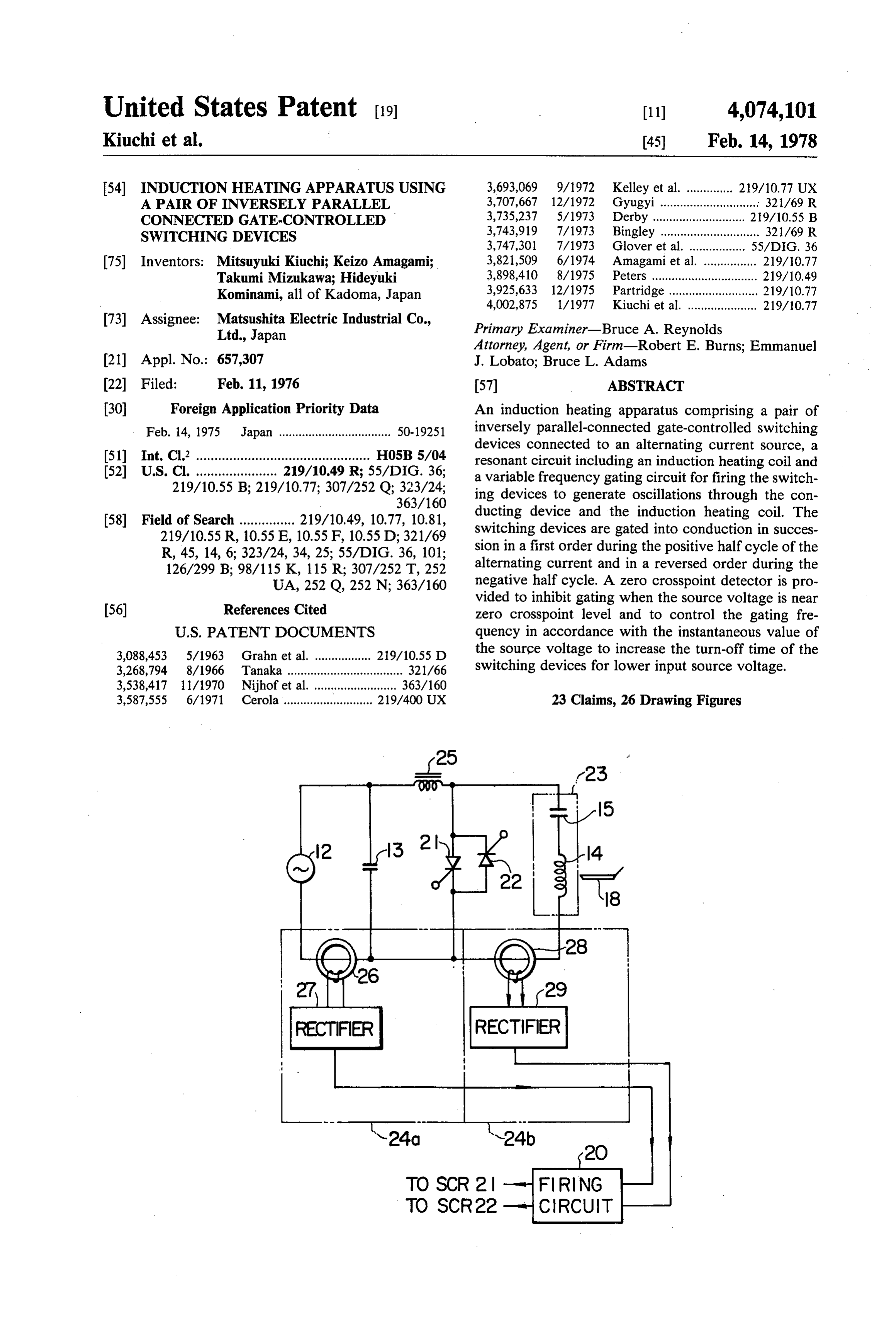
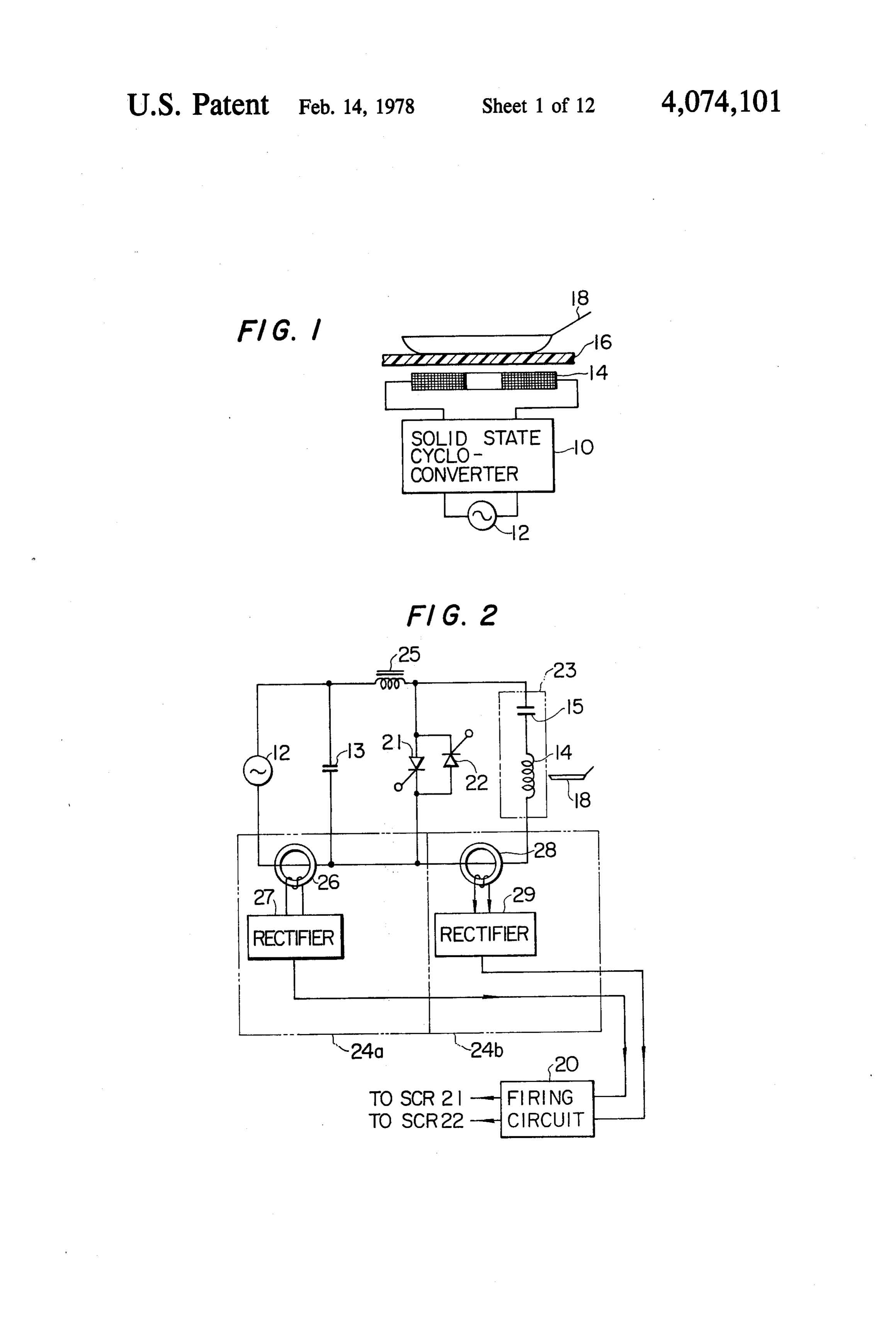
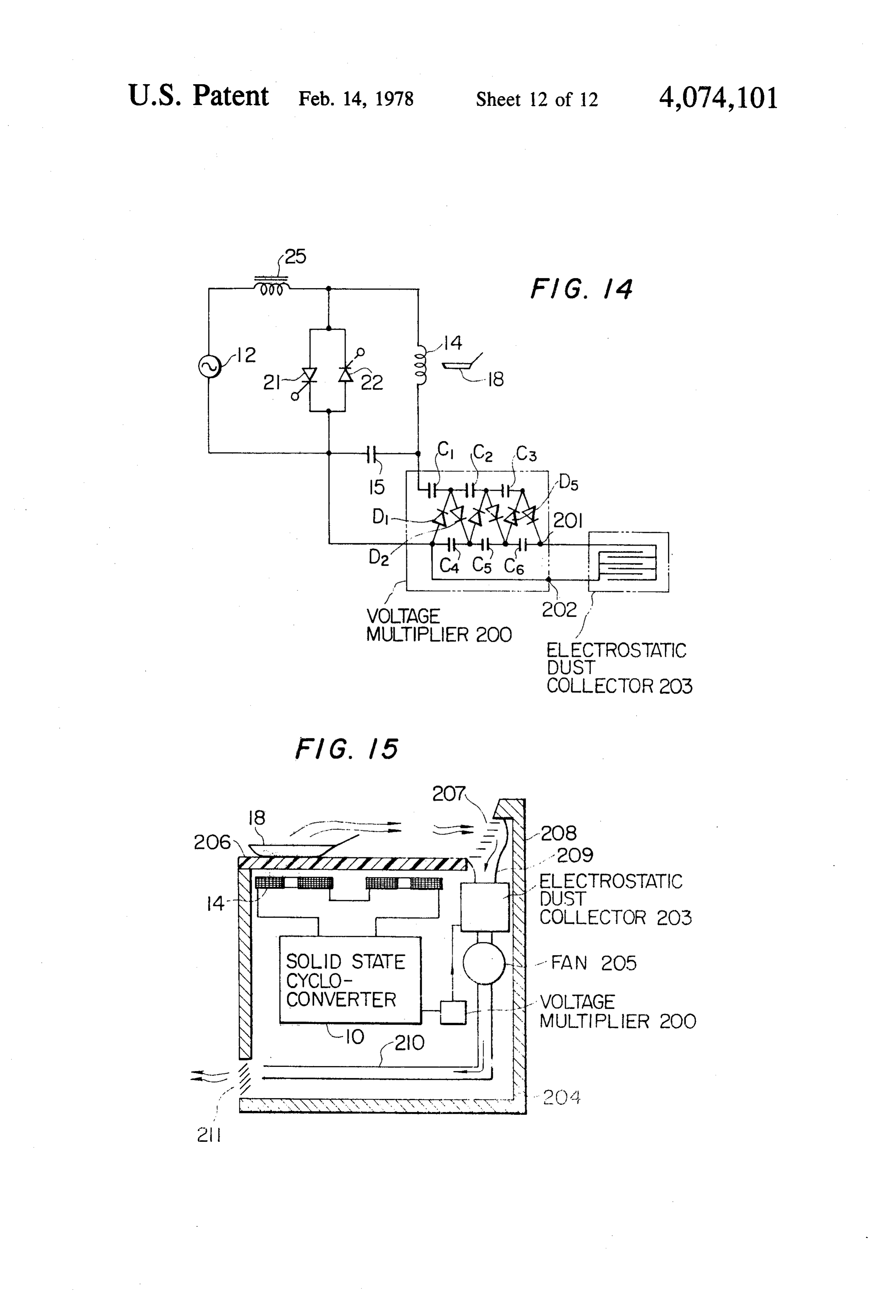
FIG. a circuit diagram showing another embodi consequential increase in cost and a greater loss of the cycloconverter isinconverted which the power output from into a high tension power due to inefficient operation have prevented the unidirectional voltage for establishing widespread use of induction heating apparatus for static field for dust collecting purposes; aandhigh electro household applications. FIG. 15 is a view illustrating the arrangement of the SUMMARY OF THE INVENTION various components of the circuit of FIG. 14. It is an object of the present invention to provide an DESCRIPTION OF THE PREFERRED improved induction heating apparatus which comprises EMBODIMENTS a cycloconverter including a pair of inversely parallel Referring now to FIGS. 1 to 7 of the drawings, a first connected gated conducting devices and a novel gating 45 preferred embodiment of the present invention is illus circuit for gating the switching devices in predeter trated. The induction heating apparatus of FIG. 1 com mined orders in synchronism with each half cycle of the prises generally a solid state cycloconverter 10 ener voltage of alternating current source. gized by a commercial AC power source 12 and an It is another object of the invention to provide an induction heating coil 14 disposed underside of a non induction heating apparatus which eliminates the need 50 metallic utensil support 16 on which a metal panload 18 of full-wave rectification to thereby reduce the number is placed. The cycloconverter 10 generates a high fre of components required and increase the overall effi quency signal in the ultrasonic range to excite the in ciency of the apparatus. duction heating coil 14 which electromagnetically cou It is a further object of the invention to provide an ples with the pan load 18. As shown in FIG. 2, the solid improved induction heating apparatus which is free 55 state cycloconverter 10 comprises a pair of gated semi from generating unwanted radio frequency components conductor conducting devices such as silicon-con which would produce radio inteference to nearby elec trolled rectifiers 21 and 22 inversely parallel connected trical appliances. to first and second terminals 31, 32 of the AC voltage BRIEF DESCRIPTION OF THE DRAWINGS 60 source 12, a resonant circuit 23 including the induction heating coil 14 and a resonant capacitor 15 in parallel
These and other objects, features and advantages of circuit relationship with the SCR pair, and a firing cir the present invention will be understood from the foll cuit 20 which generates gating-on pulses for the SCR's lowing detailed description when read in conjunction 21 and 22. A filter induction 25 is inserted between with the accompanying drawings, in which: terminal 31 and the oscillatory loop comprising SCR FIG. 1 is a schematic diagram of an embodiment of 65 pair and resonant circuit 23, and a filter capacitor 13 the invention; connected across the filter inductor 25 and the SCR pair FIG. 2 is a circuit diagram of an embodiment of the 21, 22, to eliminate high frequency energization current invention in which a pair of inversely parallel con generated from the oscillatory loop to prevent it from
Page 15
disturbing the alternating current source 12. Between chosen at respective levels slightly above and below the the terminal 32 and capacitor 13 is connected an input zero voltage level to provide an inhibit interval during power detector 24a which includes a current trans which no firing occurs. The waveforms generated by former 26 which detects the current flow from the the level detectors 40 and 41, as illustrated in FIG. 5, are power supply 12 to the oscillatory loop or output cir fed to the NOR gate 42 to produce a gate control pulse cuit. The detected current is converted into a DC volt for an inhibit gate 35.
age by means of a rectifier 27 and fed into a firing circuit The pulse generator 34 output is connected to a delay 20. An output power detector 24b of similar configura circuit 38 and to one input of a pulse distributer 39. The tion as 24a is connected in the oscillatory loop to sense pulses supplied to the delay circuit 38 are delayed by an the output current, the output from the detector 24b 10 interval determined by the tuned frequency of the reso being connected to the firing circuit 20. nant circuit 23. The flip-flop 37 is triggered from its In FIG. 4, the firing circuit 20 includes a first compar quiescent state at the leading edge of a pulse from the ator or differential amplifier 30a and a second compara NOR gate 42 and back to its quiescent state at the lead tor or differential amplifier 30b. The output from the ing edge of the next pulse to generate a symmetrical input power detector 24a is connected to the first com 15 square wave pulse (FIG. 7c). The square wave pulse is parator 30 to compare the input power level with a applied to the pulse distributer 39 to alternate the order user's setting value and generate an output when the of firing the SCR's 21 and 22 at the beginning of each input level is lower than the user's setting. The compar half cycle of the source voltage. ator 30a feeds its output to a variable frequency oscilla In FIG. 6 the pulse distributor 39 is shown compris tor 33 such as voltage-controlled oscillator of the type 20 ing a number of logic gates. The pulses directly supplied NE555V available from Signetics Corp. to control its from the pulse generator through inhibit gate 35 are frequency in such manner that when the input power connected to AND gates 50 and 53, while the pulses level is lower than the preset value in case where a false from the delay circuit are connected to AND gates 51 load is placed on the apparatus, the oscillator is brought and 52. The output from the flip-flop 37 is directly to a lower frequency in order to reduce the power 25 coupled to the AND gates 50 and 52 and its inverted delivered to the false load. The output power detector output is coupled to the AND gates 51 and 53. The 24b connects its output to the second comparator 30b AND gates 50 and 52 are switched during the positive for comparison with the desired power level to produce half cycle of the AC input wave, while the AND gates a difference signal which is also applied to the oscillator 51 and 53 are switched during the negative half cycle of 33. Excessive output power will be compensated for by 30 the AC input. During the positive half cycle of the input operating the oscillator 33 at a lower frequency, and waveform, the non-delayed pulses from inhibit gate 35 when more power is desired the frequency will be in are passed through the switched gate 50 to the control creased. In order to assure satisfactory firing of the gate gate of SCR 21 via OR gate 54 and the delayed pulses controlled switching devices 21 and 22 to sustain oscil are passed through the switched gate 52 to the control lations in the cycloconverter circuit 10 at the beginning 35 gate of SCR 22 via OR gate 55 so that SCR 21 is gated of each half cycle of input source voltage, the variable on repetitiously by the non-delayed pulses while SCR frequency oscillator 33 is connected to the prime volt 22 is gated on repetitiously at the same rate as SCR 21 age source 12 in such manner than when the instanta but at later times by the delayed pulses. The oscillations neous source voltage is near the zero voltage level, the so occurred in the cycloconverter 10 are slightly below oscillator frequency is reduced to a minimum to allow the tuned frequency of the resonant circuit 23. sufficient quiescent time for the charging capacitor 15 During the negative half cycle of the AC input volt during the period of the low input voltage. The variable age, the non-delayed pulses are passed through the frequency oscillator 33 has its output connected to a switched gate 53 to SCR 22 via OR gate 55, while the pulse generator 34 to supply it with variable frequency delayed pulses are passed through the switched gate 51 oscillation signal, the pulse generator 34 converting the 45 to SCR 21 via OR gate 54, so that SCR 22 is fired earlier input oscillations into a train of pulses suitable for firing than SCR 21. Therefore, when the input terminal 32 is the gate controlled switches 21 and 22. A firing pulse positive with respect to terminal 31, SCR 22 is fired by inhibiting circuit formed by an inhibit gate 35 and a zero the non-delayed pulses to trigger high frequency oscil crossover point detector 36 is provided to prevent the lations and SCR 21 is fired to allow the next half cycle firing of SCR's 21 and 22 when the alternating current 50 of the oscillation current to flow therethrough. source voltage is near zero voltage point between suc The operation of the circuits of FIGS. 2 and 4 may cessive half waves of the input voltage waveform. The best be understood by reference to FIG. 7. Assume that inhibit gate 35 is connected to the output of the pulse the terminal 31 is positive with respect to terminal 32 generator 34 to inhibit the passage of pulses there and the capacitor 15 has charged up to a voltage suffi through by the control pulse supplied from the zero 55 cient to produce an oscillating current through the crossover point detector 36. The detector 36 comprises resonant circuit should SCR 21 be gated on (FIG. 7d), two level detectors 40 and 41 and a NOR gate 42. The the turn-on of SCR 21 will cause the charge stored on level detector 40 has its one input coupled to the volt the capacitor 15 to be oscillated through the now con age source 12 and has its other input connected to a ducting SCR 21 and through the resonant circuit 23 in reference voltage of positive polarity (+V) to pro a positive half cycle of the oscillation to reversely duce a signal when the inputsource voltage is above the charge the capacitor 15. The reverse polarity charge on reference voltage. The level detector 41, on the other capacitor 15 will cause a reverse current flow in the hand, has its one input coupled to the voltage source 12 negative half cycle of the oscillation when SCR 22 is while its other input coupled to a reference voltage of gated on by the successive gating-on pulse which oc negative potential (-V) so that an output signal is 65 curs at the delayed timing provided by the delay circuit produced when the input voltage is greater than the 38 (FIG. 7e). During the reverse current flow SCR 21 negative reference voltage during its negative half cy will be reverse biased and will be maintained off. After cle. The positive and negative reference voltages are completion of the oscillation SCR 22 will be turned off
Page 16
by the positive source voltage before the next pulse The oscillating current will become as shown in FIG. triggers SCR 21 to cause successive oscillations. This 7f. From an examination of FIGS. 7a and 7f, it is noted process will repeat as long as the source voltage retains that the oscillatory energization current flow that oc the same voltage polarity. curs during the reverse half cycle of each oscillation During the next negative half cycle of the source develops a current envelope as indicated by dashed voltage, the order of application of gating-on pulses is lines which is 180° out of phase with respect to the input reversed so that SCR 22 will be fired earlier than SCR voltage waveform. This means that the power resulting 21. from the product of relatively phase displaced voltage In the parallel circuit arrangement of FIG. 2 in which and current is negative and being returned to the power capacitor 15 is parallel connected with the SCR pair 21, O supply. This is an advantageous effect of the cyclocon 22 to voltage source 12, a problem will be encountered verter of the present invention from the power saving when the input AC voltage is at the beginning of each standpoint.
half wave, if a gating-on pulse is applied when the Where it is desired to provide a greater amount of charge stored on capacitor 15 is insufficient to sustain power than is provided by a pair of gated conducting oscillations. Under such conditions, the gated SCR will 15 devices 21 and 22, two pairs of inversely parallel con remain conductive to provide a short circuit across the nected SCR's may be employed as shown in FIG. 8. In resonant circuit 23 so that the charge stored on the FIG. 8a, a first pair of inversely parallel connected capacitor 15 will be exhausted. This inoperative condi SCR's 71 and 72 is connected in series to a second pair tion will persist until change occurs in the voltage po of inversely parallel connected SCR's 73 and 74, the larity which causes the conducting SCR to be reversely 20 first and second SCR pairs being connected across the biased to thereby turn it off. . input terminals 31 and 32 via a filter inductor 25. A For this purpose the inhibit gate 35 prevents the ap resonating circuit 23 comprising a capacitor 26 and an plication of gating-on pulses during the time while the inductor 14 is coupled across the second pair of SCR's source voltage is below a predetermined level, while 73 and 74 in parallel thereto and in series to the first pair allowing the capacitor 15 to be charged up to a voltage 25 of SCR's 71 and 72. A power detector 24 having a level sufficient to sustain oscillations. The variable fre current transformer 26 and a rectifier 27 is coupled to quency oscillator 33 in turn causes the intervals be the terminal 32 to detect the current representing the tween successive early gating-on pulses to vary in ac power withdrawn from the inductor 14 and supply the cordance with the source voltage. While the source detected signal to a firing circuit 20 shown in FIG. 9. voltage is low, the longer intervals are provided to 30 The firing circuit 20 is generally similar to that shown in allow the capacitor 15 a sufficient quiescent time to FIG. 4 except that a reversible ring counter 70 is em build up charge. ployed rather than a circuit consisting of the delay cir The resonating circuit 23 may be coupled in a series cuit 38 and the pulse distributer 39 of FIG. 4. The out circuit relationship with the SCR pair 21, 22 as shown in put from the pulse generator 34 is connected to the FIG. 3. In operation, assume that terminal 31 is positive 35 input of ring counter 70 which in response to the input with respect to terminal 32, and SCR 21 is turned on. pulse activates one of its output terminals 81 to 84 in Upon the turn-on of SCR 21, the capacitor 15 will be succession so that the input pulse is distributed as indi positively charged to the source voltage and an oscilla cated by a series of waveforms in FIG. 10. During the tory current will flow through the now conducting positive half cycle of the alternating current at source SCR 21 and through the resonating circuit 23 and com 12, the ring counter 70 operates to distribute the pulses pletes its first half cycle when the capacitor 15 is re in the order of its output terminals 81, 82,83 and 84. The versely charged whereupon the oscillatory current will output of the zero crossover point detector 36 is also flow in reverse direction when SCR 22 is gated on by connected to the ring counter 70 to reverse its order of the delayed gating-on pulse during the next half cycle of appearance of outputs at the beginning of the next nega the oscillation. The frequency of the oscillation is 45 tive half cycle of the source voltage. The ring counter slightly below the tuned frequency of the resonating 70 reverses its order of counting upon receipt of an circuit 23, as in the parallel circuit arrangement of FIG. inhibit pulse. A detailed description of the reversible 2. ring counter is found in an article entitled "Reversible Similarly, the problem as discussed above in connec Ring Counters Utilizing The Silicon Controlled tion with FIG. 2 will occur when gating of SCR's oc 50 Switch' by Robert M. Muth et al., Application Note curs at low source voltages. Under such conditions, the 90.58, 4/66 published by General Electric Company. gated switching device will remain conductive until it Assume that the input terminal 31 is positive with will be turned off by a reverse voltage in the next half respect to the terminal 32, the ring counter 70 will place cycle of the source voltage. The inhibit circuit arrange a first pulse on the output terminal 81 to thereby turn on ment and the variable frequency oscillations previously 55 SCR 71 causing the capacitor 26 to be positively described in connection with the circuit of FIGS. 2 and charged to the source voltage. In FIG. 10, the first 4 are also employed effectively to avoid such undesir pulses 81-1 on output terminal 81 causes a current 81-2 able effects. to flow through the conducting SCR 71. In succession In this series circuit arrangement of FIG.3 a capaci SCR 72 will be gated on by the pulse 82-1 which ap tor 13 is connected across the terminal 32 and a point pears before the current 81-2 is still flowing through the intermediate the filter inductor 25 and capacitor 15 to SCR 71. Although the gating-on pulse 82-1 is being provide a path for the oscillatory current. A reset induc applied, the SCR 72 conducts no current until the cur tor 19 is connected across the capacitor 15 to release the rent 81-2 falls to zero. The charge stored on the capaci charge stored thereon into 19. The power detector 24b tor 26 will be oscillated through the conducting SCR 71 is connected in series with terminal 32 and the SCR pair 65 and through the resonating circuit 23 and capacitor 13 21, 22. The power detector 24b couples its output to the and reversely charge the capacitor 26 to cause a reverse comparator 30b of firing circuit 20 to control the output current flow through the conducting SCR 72. While the power level at the desired value. reverse current is flowing, SCR 73 will be gated on the
Page 17
gating-on pulse 83-1 to conduct the reverse current to produce an oscillatory current through the conduct during the rest of the negative half cycle of the oscilla ing SCR's 72 and 71 and through the load inductor 77. tion. While SCR 73 is still conducting, SCR 74 will be The cycloconverter 10 is further modified into a form rendered conductive by the next pulse 84-1. Therefore, as shown in FIG. 8c to provide a perfect sinusoidal currents as indicated in waveforms 82-2 and 83-2 will be output waveform. In this modified form, inductors 78 conducted respectively by the SCR's 72 and 73. Capaci and 79 are connected in series between a first SCR pair tor 26 will then be charged positively to cause a current 71, 72 and a second SCR pair 73, 74 in a first circuit 84-2 to flow through the conducting SCR 74. SCR 71 path. Capacitors 75 and 76 are connected in series in a will be again gated into conduction by the next pulses second circuit path which is connected in parallel with 81-3 to replenish a charge on the capacitor 26 causing a 10 the first circuit path. A first resonating circuit 85 com current 81-4 to flow in order to sustain oscillations in prised by an induction heating coil 77 and a capacitor 80 the subsequent period. in a series circuit relation is connected between a point During the next negative half cycle of the source intermediate the inductors 78 and 79 and a point inter voltage, the firing order is reversed. However, the ini 15 mediate the capacitors 75 and 76. Capacitor 75 and tial gating-on pulses supplied to SCR's 74 and 73 have inductor 78 are tuned to a predetermined frequency to no effect on the operation of cycloconverter since there form a second resonating circuit 86. Capacitor 76 and is no charge on the capacitor 26. The subsequent turn inductor 79 are also tuned to the first frequency to form on of SCR 72 will cause capacitor to be charged nega a third series resonant circuit 87. The first resonant tively to initiate oscillations which will be sustained by 20 circuit 77 is tuned to a frequency which is double the subsequent conduction of SCR's 71,74 and 73. frequency of either circuit 86 or 87. When the source voltage is slightly above the inhib It is often desirable to provide a plurality of induction ited level, the intervals between successive gating-on in FIG. coils heating in a series circuit relationship as illustrated pulses are prolonged to allow the capacitor to be trated in11a and in a parallel circuit relationship as illus FIG. 11b. In the series circuit arrangement of charged up sufficiently to sustain oscillations, FIG. 11a the current flow through induction heating It is to be noted that in the firing process SCR's 71 25 coils 91, 92, 93 and 94 is maintained constant when a and 72 are simultaneously gated on in the transitory desired power level is attained. The power detector 23 period when the oscillatory current reverts its direction senses the current through the coils 91 to 94 and feeds a of flow, and SCR's 72 and 73 are also simultaneously voltage signal gated on in the transitory period during which currents 30 firing circuit 20.representing
The the detected current to the comparator 30 of the firing circuit 82-2 and 83-2 are flowing, and therefore, a smooth tran 20 (FIG. 4) compares it with a user's setting value to sition of current conduction is achieved which results in a waveform generally similar to an ideal sinusoidal the actual power delivered to the load and thebetween provide an output representing the difference desired wave. Therefore, the higher frequency harmonics such power level. The output from the comparator 30 con as R-F components are effectively suppressed and as a 35 trols the frequency of the oscillator 33 in such manner result no filter circuit for filtering out the R-F compo that when the actual power is lower than the desired nents is necessary. level the frequency is raised until the desired level is A modification of the cycloconverter 10 is illustrated reached and when the actual power is higher than the in FIG. 8b in which series-connected capacitors 75 and desired level the frequency is lowered to attain the 76 are connected across the first and second SCR pairs desired level so that the average value of the energiza in parallel, and an induction heating coil 77 is connected tion current through coils 91 to 94 is held constant for a between a point intermediate the first and second SCR given level of user setting regardless of the number of pairs and a point intermediate the capacitors 75 and 76. energized or switched-on induction heating coils. In operation, assume that the input terminal 31 is posi In the arrangement of FIG. 11b, induction heating tive with respect to the terminal 32 and capacitors 75 45 coils 91 to 94 are connected in parallel to the SCR pair and 76 are consequently charged positively. When SCR 21, 22 in which the voltage developed across the paral 71 is gated into conduction by a pulse 81-1, a forward oscillating current 81-2 will flow through the conduct lel-connected coils 91 to 94 is sensed by a power detec tor formed by a rectifier 95 connected across the coils ing SCR 71 and through the load inductor 77 to re 91 to 94. The rectified voltage represents the power versely charge the capacitor 75. During the forward 50 delivered to the load and is applied to the comparator current flow SCR 72 will be applied with a pulse 82-1 30b of firing circuit 20 (FIG. 4). As described in connec and upon the reversal of the polarity of capacitor 75 a tion with the circuit of FIG. 11a, the frequency of the reverse current 82-2 will pass through the conducting oscillator 33 will be controlled to attain the desired SCR 72. While the SCR 72 is conducting, SCR 73 will power level and the average value of the voltage across be gated into conduction by the pulse 83-1, as a result of 55 the coil 91 to 94 is maintained constant for a given level which the charge stored on capacitor 76 is oscillated of user setting regardless of the number of energized through the conducting SCR 73 and through inductor induction heating coils.
77 producing a reverse current 83-2 in its first oscillat In the arrangements of both FIGS. 11a and 11b, the ing half cycle and then a forward current 84-2 when electromagnetic coupling between the load and each SCR 74 is gated on by a pulse 84-1. In the negative half 60 induction heating coil is achieved by an elevating mech cycle of the source voltage, capacitors 75 and 76 are anism as shown in FIG. 11c in which each of the induc charged negatively and the firing order is reversed. tion heating coils 91 to 94 is supported by a cross-arm SCR 74 is gated into conduction in the first place to elevating mechanism 96 which may be actuated manu cause the charge stored on capacitor 76 to oscillate ally in such manner that the air gap between the load 18 through the conducting SCR 74 and inductor 77 in its 65 and each coil is varied to individually control the power first half cycle and then through the successively actually delivered to the load on each coil. turned-on SCR 73 in its second half cycle. SCR 72 and The high frequency electrical oscillations of the then SCR 71 will be gated into conduction in succession power converter 10 can also be utilized to generate a
Page 18
high tension unidirectional voltage in addition to gener has an equal inductance to that of induction heating coil ating electromagnetic flux for induction heating with 14 to provide oscillation at the same frequency when the use of a step-up transformer having a fewer number the switch 112 is connected to either side of its station of turns than is required to generate from a low fre ary contacts. In FIG. 13b, the induction heating coil 14 quency source such as obtained from the commercial is carried by an elevating mechanism 91 as described in AC outlet. connection with FIG. lic. The elevating mechanism 91 An embodiment shown in FIGS. 12 and 13 illustrates is in turn disposed on the top wall of the shielded cham a combination in which the induction heating apparatus ber 111 of microwave oven and housed in the same previously described is housed in the same compart casing 110 with the magnetron microwave oscillator ment with a microwave oven of a conventional type. In 10 100. The casing 110 has on its top wall a non-metallic FIG. A2a, a step-up transformer 101 has its primary utensil support plate 16 flush with the other portion of winding connected across the terminals of the resona the top wall and located over the induction heating coil tion capacitor 15 and its secondary winding coupled to 14. In this arrangement foodstuff is placed in the cham a rectifier circuit 102 including a diode 103 and a ber 111 when heated by the microwave radiant energy smoothing capacitor 104. The rectifier 102 converts the 15 and on the support plate 16 when heated in the induc high frequency, high tension voltage developed across tion heating mode. The height of the induction heating the secondary of transformer 101 into a high tension coil 14 is adjusted manually by a mechanical linkage unidirectional voltage which is supplied to the anode (not shown) which is accessible to the user. and the heated cathode of a magnetron 260. The cath Another example of utilizing the ultrasonic frequency ode of magnetron 100 is supplied with a low voltage AC 20 oscillations of the power convertor 10 is shown in current from a transformer 105 coupled to the AC FIGS. 14 and 15. In FIG. 14, a voltage multiplier 200 is power source 12. The magnetron 100 generates oscilla connected across the capacitor 15 of resonant circuit 23 tions at a frequency in the microwave region which is to develop a high tension DC voltage at the output radiated to an electromagnetically shielded chamber terminals 2011 and 202 to which is connected an electro 111 of a microwave oven housing 110 through a wave 25 static dust collector 203. The voltage multiplier 200 guide 106 (FIG. 13a). The chamber 111 is constructed comprises a first group of series-connected capacitors of aluminum and electrically connected to ground for C1 to C and a second group of series-connected capaci shielding purposes. A non-metallic utensil support plate tors C4 to C6 and a plurality of diodes D1 to Ds. Each of 107 is disposed on the the lower portion of the chamber the diodes is connected between the junctions of the 111 at a position spaced from the bottom wall thereof. 30 first and second groups of capacitors and alternately The induction heating coil 14 is disposed within the poled in opposite directions so that capacitors of the space between the support 107 and the bottom wall of first group are connected by the diodes to the capacitors the chamber 111 and connected to the power converter of the second group in staggered relation to each other. i0 previously described. Since aluminum is a non-mag Each of the capacitors in either group stores charge netic material, no heat will substantially be produced by 35 which builds up increasingly toward the output termi the high frequency electromagnetic field set up by the nal 2011. The dust collector 203 is of the conventional induction heating coil 14 in the walls of the chamber design which includes a plurality of oppositely facing 1A close to the coil 14. The converted high tension DC electrodes to which is connected the high DC voltage voltage may be adjusted by varying the electromagnetic obtained from the voltage multiplier 200 to establish a coupling between the primary and secondary windings strong electric field between each pair of electrodes of the step-up transformer 101 as indicated by the arrow through which dust may be permitted to pass. FIG. 15 in the drawings. The non-metallic support 107 serves as shows an arrangement of the dust collector 203 in the a common surface for metallic utensil for induction induction heating apparatus as previously described. heating and non-metallic utensil for heating under the The dust collector 203 is disposed within a housing 204 influence of the microwave radiant energy. Therefore, 45 having a non-metallic utensil support top 206, air inlet it is important to indicate to the user that when the grille 207 provided in the opening between the top 206 apparatus is operated in the induction heating mode the and the rear panel 208 and has an air inlet connected to utensil be of metallic ferrous material while in the mi the air inlet grille 207 by a passage 209 and an air outlet crowave mode of operation the utensil be of non-metal side connected to a fan 205 disposed in a duct 210 which lic material. Since the microwave radiant energy pro 50 leads to an air outlet grille 211 provided on the lower duces heat in the foodstuff at uniform temperature . part of the housing 204. The induction heating coil 14 throughout, while the induction heating produces heat which is energized by the output from power convertor in the material of utensil which in turn heats up the 10 is located underside of the utensil support top 206 on foodstuff therein progressively from the outer surface, which a metallic utensil 18 may be placed. When the fan different cooking conditions are provided to achieve 55 15 is energized, a forced air flow will be produced different results, for example, the induction heating through the air inlet grille 207 to the outlet grille 211. produces a burning effect which causes a slight burning Objectionable fumes and ordours produced from the on the surface of the foodstuff so that different taste utensil 18 on the top plate 206 will be inducted through may be achieved from that provided by microwave the inlet grille 207 and passed through the dust collector heating. 203 where they will be charged by the high electrostatic A changeover switch 112 may be provided to operate field between the collecting electrodes and adhered either in the induction heating mode or in the micro thereto This is particularly advantageous when food wave heating mode. The switch 12 may be a transfer stuff is fried which results in producing a considerable type as shown in FIG. 12b and has a moving contact amount of greasy material.
connected between the resonant-circuit 23 and the coil 65 What is claimed is:
14 and switched to provide connection between the 1. An induction heating apparatus comprising, a pair resonant circuit 113 and the primary winding of the of input terminals connectable in use to a source of low transformer 101. In this example, the transformer 101 frequency alternating voltage, at least a pair of first and
Page 19
second gate-controlled unidirectional conducting de to detect a voltage developed thereacross and said fre vices inversely parallel connected to the input termi quency controlling means is coupled to said comparing nals, means sensitive to the polarity of said alternating means to control the gating frequency of said gate-con voltage for generating an output indicative of the polar trolled conducting device in the direction of the devia ity of the alternating voltage, means for gating on said tion of said detected voltage from said fixed reference to first and second gate-controlled unidirectional conduct minimize said deviation so that said voltage across said ing devices in succession at a high frequency in a given induction heating coils is maintained constant regardless order in response to the output from said polarity sensi of the magnitude of power delivered to loads placed tive means indicating one polarity of the alternating over said induction heating coils.
voltage and in succession at the high frequency in a 10 8. An induction heating apparatus as claimed in claim reversed order in response to the output from said po 7, further comprising a vertically movable support on larity sensitive means indicating the opposite polarity of which each of the first and second induction heating the alternating voltage, and high-frequency commutat coils is disposed, and means for adjusting the spacing ing circuit means including an induction heating coil between the associated load and the support. and a capacitor in series thereto responsive to a current 15 9. An induction heating apparatus as claimed in claim produced when one of the gate-controlled conducting 4, further comprising a second induction heating coil devices is gated on for producing in succession a com connected in series with the first induction heating coil, mutating current that flows through said commutating and wherein said electrical quantity detecting means is circuit means and the subsequently gated-on gate-con connected in series with said induction heating coils to trolled conducting device in the opposite direction. 20 detect a current passing therethrough and said fre 2. An induction heating apparatus as claimed in claim quency controlling means is coupled to said comparing 1, further comprising means responsive to the instanta means to control the gating frequency of said gate-con neous value of the source of alternating voltage for trolled conducting devices in the direction of the devia controlling the gating frequency of said gate-controlled tion of said detected current from said fixed reference to conducting devices substantially in proportion to said 25 minimize said deviation so that said current is main instantaneous value of the source voltage. tained constant regardless of the magnitude of power 3. An induction heating apparatus as claimed in claim delivered to loads placed over said induction heating 1, further comprising means for detecting when the coils.
instantaneous value of the source of alternating voltage 10. An induction heating apparatus as claimed in is below a predetermined value and means for inhibiting 30 claim 1, wherein said pair of gate-controlled conducting said gate-controlled conducting devices in response to devices is connected in series to the commutating cir the output of said detecting means. cuit means.
4. An induction heating apparatus as claimed in claim 11. An induction heating apparatus as claimed in 1, further comprising electrical quantity detecting claim 1, wherein said pair of gate-controlled conducting means for detecting an electrical quantity representative 35 devices is connected in parallel with the commutating of power delivered to a load in overlying relation with circuit means.
said coil, means for comparing the detected electrical 12. An induction heating apparatus as claimed in quantity with a fixed reference representing and corre claim 1, further comprising, in combination therewith, sponding to a desired power level to detect the devia means for converting the current flowing through said tion of the power delivered to said load from the desired commutating circuit means into a high tension DC volt power level, and means for controlling the gating fre age, a housing having an electromagnetically shielded quency of said gate-controlled conducting devices in chamber therein made of a metal of substantially non the direction of the deviation of said delivered power magnetic material, a magnetron having a heated cath from said desired power level so as to minimize said ode and an anode energized by said high tension DC deviation. 45 voltage to produce high frequency oscillations in the 5. An induction heating apparatus as claimed in claim microwave region, and means for emitting microwave 4, further comprising a second induction heating coil energy to said chamber.
connected in series to the first induction heating coil to 13. An induction heating apparatus as claimed in form a series resonant circuit so that the first and second claim 12, wherein said induction heating coil is disposed induction heating coils are energized by a high fre 50 on top of the housing.
quency energization current of equal magnitude, and 14. An induction heating apparatus as claimed in wherein said electrical quantity detecting means is con claim 13, further comprising a vertically movable sup nected in said series resonant circuit to detect a current port on which the induction heating coil is disposed and flow therethrough and said frequency controlling means for adjusting the height of the induction heating means is coupled to the electrical quantity detecting 55 coil with respect to a load placed in overlying relation means to control the frequency of said firing pulses such therewith.
that said current flow is maintained constant regardless 15. An induction heating apparatus as claimed in of the magnitude of power delivered to said load. claim 12, wherein said converting means comprises a 6. An induction heating apparatus as claimed in claim step-up transformer having its primary winding con 5, further comprising a vertically movable support on nected to receive the current flowing through said in which the induction heating coil is disposed, and means duction heating coil, a rectifier connected to the sec for adjusting the spacing between the load and the sup ondary winding of the transformer to generate said high port. tension DC voltage, and means for adjusting electro 7. An induction heating apparatus as claimed in claim magnetic coupling between the primary and secondary 4, further comprising a second induction heating coil 65 windings of the transformer.
connected in parallel with the first induction heating 16. An induction heating apparatus as claimed in coil, and wherein said electrical quantity detecting claim 15, wherein said adjusting means is connected in means is connected across said induction heating coils the commutating circuit means.
Page 20
17. An induction heating apparatus as claimed in sponse to the output from said polarity sensitive claim 12, wherein said induction heating coil is disposed means indicating the opposite polarity of the alter on the botton wall of the shielded chamber, and nating voltage; and wherein a non-metallic utensil support is disposed in high frequency commutating circuit means including overlying relation with the induction heating coil. 5 an induction heating coil and a commutating ca 18. An induction heating apparatus as claimed in pacitor in series thereto responsive to a current claim 1, further comprising means for converting the produced when one of the gate-controlled switch current flowing through said induction heating coil into ing devices is gated on for producing in succession a high tension DC voltage, a housing having a nonme a commutating current that flows through said tallic top wall and side and botton walls, an electro 10 commutating circuit means and a subsequently static precipitator energized by said high tension DC gated-on switching device. voltage, and means located adjacent said top wall for intaking air to said electrostatic precipitator, and claim An 21.
induction heating apparatus as claimed in wherein said commutating circuit means is wherein the induction heating coil is disposed in under connected across one of said first and second pairs of lying relation with said top wall of the housing. 15 switching devices.
19. An induction heating apparatus as claimed in 22. An induction heating apparatus as claimed in claim 18, wherein said converting means comprises a claim voltage multiplier comprising a pair of first and second prises 20,a wherein said commutating circuit means com first and a second capacitive element connected groups of series connected capacitors and a plurality of diodes each being connected across a point of connec 20 in series across said first and second pairs of switching tion between successive capacitors of the first group devices, and wherein said induction heating coil is con and a point of connection of successive capacitors of the nected between a point intermediate the first and sec second group, said diodes being alternately poled in ond pairs of switching devices and a point intermediate opposite directions. the first and second capacitive elements. 20. An induction heating apparatus comprising: 25 23. An induction heating apparatus as claimed in a first pair of inversely parallel connected first and claim 20, wherein said commutating circuit means com second gate-controlled switching devices, a second prises a pair of first and second inductive elements con pair of inversely parallel-connected third and nected in series to said first and second pairs of switch fourth gate-controlled switching devices, the first ing devices, a pair of first and second capacitive ele ments connected in series across said first and second and second pairs being connected in use in series to 30 pairs a source of low frequency alternating voltage, and of switching devices, a first resonating circuit wherein the first and third switching devices are including said induction heating coil connected be poled in the same direction of conduction and the tween a point intermediate the first and second induc second and fourth switching devices are poled in tive elements and a point intermediate the first and the opposite direction of conduction; 35 second capacitive elements, the first capacitive and means sensitive to the polarity of said alternating inductive elements being connected in a second resonat voltage for generating an output indicative of the ing circuit configuration, the second capacitive and polarity of the alternating voltage; inductive elements being connected in a third resonat means for gating on said first, second, third and ing circuit configuration, the first resonating circuit fourth switching devices in succession in a given being tuned to a frequency which is double the fre order in response to the output from said polarity quency to which the second and third resonating cir sensitive means indicating one of the polarity of the cuits are tuned.
alternating voltage and in a reversed order in re :
Provenance
- Collection
- Cited prior art
- Original PDF
- patentimages.storage.googleapis.com →
- Filed
- 1976-02-11
- Pages
- 20
- Method
- pdftotext (the PDF's own text layer) + pdftoppm 300dpi page scans
- Source
- Google Patents bibliographic record
- Granted
- 1978-02-14
- Inventors
- Mitsuyuki Kiuchi; Keizo Amagami; Takumi Mizukawa; Hideyuki Kominami; Matsushita Electric Industrial Co Ltd
- Transcribed from
- patentimages.storage.googleapis.com →