patent · US3832488
Non-impact printer
27 August 1974
Page 1 — bibliographic record
United States Patent (19) [11] 3,832,488 Fahey et al. (45) Aug. 27, 1974 54) NON-IMPACT PRINTER Primary Examiner-Thomas A. Robinson (75) Inventors: Wm. David Fahey, Santa Clara; Attorney, Agent, or Firm-Francis L. Masselle; James Robert W. Johnson, Los Aitos, both C. Kesterson; J. Ronald Richbourg of Calif.
73 Assignee: The Singer Company, Binghampton, (57) ABSTRACT
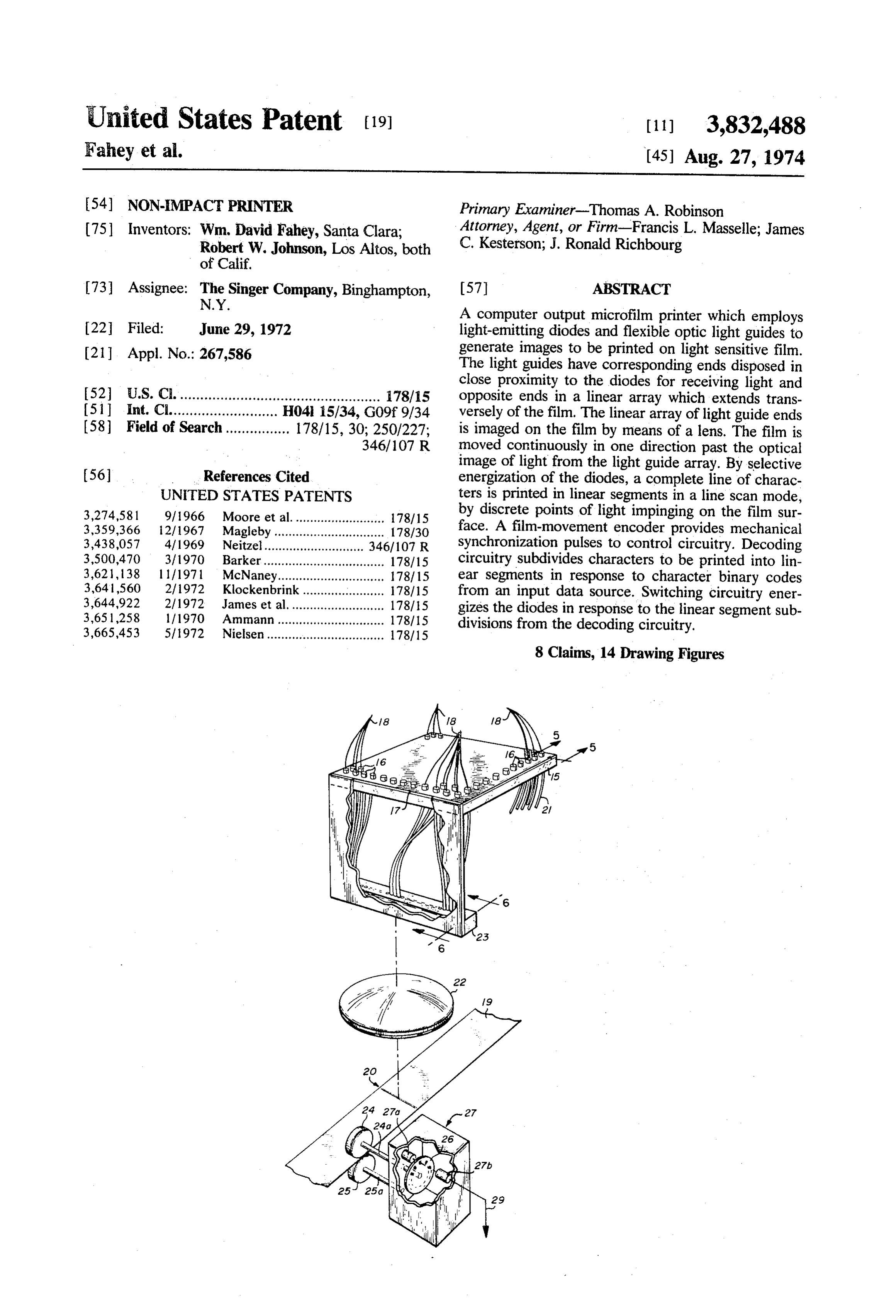
A computer output microfilm printer which employs 22 Filed: June 29, 1972 light-emitting diodes and flexible optic light guides to (21) Appl. No.: 267,586 generate images to be printed on light sensitive film. The light guides have corresponding ends disposed in close proximity to the diodes for receiving light and 52 U.S.C. .................................................. 178/15 opposite ends in a linear array which extends trans 51 int. Cl........................... H04 15/34, G09f 9/34 versely of the film. The linear array of light guide ends (58) Field of Search................ 178/15, 30; 250/227; is imaged on the film by means of a lens. The film is 346/107 R moved continuously in one direction past the optical image of light from the light guide array. By selective 56 References Cited energization of the diodes, a complete line of charac UNITED STATES PATENTS ters is printed in linear segments in a line scan mode, 3,274,581 9/1966 Moore et al.......................... 178/15 by discrete points of light impinging on the film sur 3,359,366 12/1967 Magleby............................... 178/30 face. A film-movement encoder provides mechanical 3,438,057 4/1969 Neitzel............................ 34.6/107 R synchronization pulses to control circuitry. Decoding 3,500,470 3/1970 Barker.................................. 178/15 circuitry subdivides characters to be printed into lin 3,621, 138 l l 11971 McNaney.............................. 178/15 ear segments in response to character binary codes 3,641,560 2/1972 Klockenbrink....................... 178/15 from an input data source. Switching circuitry ener 3,644,922 2/1972 James et al........................... 178/15 gizes the diodes in response to the linear segment sub 3,651,258 1 / 1970 Ammann ...... 178/15 divisions from the decoding circuitry. 3,665,453 5/1972 Nielsen................................. 178/15 8 Claims, 14 Drawing Figures
Page 2
Drawing sheet — no readable text.
Page 3
Drawing sheet — no readable text.
Page 4
PATENTE AUT 27:374 3,832,488
SHEET OF 6
TO DODE
BUFFER AND
DRIVE NO.1
- 31 4O - 47 46 56 53
SHIFT . .
REGISTER --> MEMORY BUFFER
To SERIAL 32 BIT (ODD) coNVERTER C SHIFT f
REGSTER
32 BIT 43 5/ 58 O SHIFT BUFFER 29 .
32 BT STEERING COUNTER O TO DODE O SHIFT CIRCUIT BUFFER AND REGISTER 44 DRIVE NO. 2
32 BIT
SHIFT
REGISTER /
PARALLEL
SETOSERIA
BUFFER CONVERTER
(EVEN)
Page 5
Drawing sheet — no readable text.
Page 6
Drawing sheet — no readable text.
Page 7
Drawing sheet — no readable text.
Page 8
NON-MPACT PRINTER trix in over 30 different combinations for forming only the letters of the alphabet and integers 0 to 9. The re
BACKGROUND OF THE INVENTION sult is a complex system which is, therefore, not only 1. Field of the Invention high in cost but difficult to service and maintain and statistically susceptible to failures.
This invention relates generally to a device for re The primary general object of this invention is the cording intelligence, and more particularly to a com provision of a novel COM device which overcomes or puter output microfilm (COM) device which employs at least mitigates the shortcomings of comparable prior light emitting diodes and flexible fiber optic light art devices as discussed above. guides. . O A more specific object is the provision of a novel 2. Description of the Prior Art
With new developments in the computer arts tending COM speed device which is capable of higher operating than those known heretofore.
toward progressively high speed operation, there exists a need for devices that print computer output data at device using light isemitting
Another object the provision of an improved COM diodes for recording intelli a rate which is substantially faster than prior art me 15 gence on a strip of photosensitive film which requires chanical printers. The mechanical printers currently a drastically smaller number of LED's than comparable available cannot operate at speeds commensurate with prior art devices.
computer processor operation. Therefore, many com puter systems employ various techniques for overcom A further object is to provide a LED-type COM de ing this disparity in operating speed. One technique vice as characterized in the next preceding object employed with the older computers and with many which does not require intermittent advance of the film smaller computers is to use a buffer between the pro strip. A still further object is the provision of a COM device cessor and the printer. This technique usually requires intermittent stopping and starting of the processor to which, in comparison to those previously known, is wait for the printing operation. 25 simpler in construction, lower in cost, and more reli Another technique for coping with the speed dispar able in operation.
ity is to employ several mechanical printers for record To the attainment of these and other objects the in ing output data from a single high-speed computer. A vention contemplates a COM device in which a linear third technique, commonly employed, is to store out array of discrete light points from individually control put data temporarily on high-speed devices such as a 30 lable sources is imaged transversely of a moving strip disk-drive or tape-drive unit, and later perform the of photosensitive film and the light sources are selec printing operation independently of the data process tively energized in sequential-combinations to form ing. These techniques constitute an economic waste segments of the alphanumeric characters to be re that may be mitigated substantially by employing COM corded on the film, successive segments coacting incre devices which operate at very high speeds. 35 mentally as the film moves to form complete characters Many commercially available COM devices employ of an entire line. Means are provided for advancing the a cathod ray tube and a camera system for photograph film and controlling the energization of the light ing images formed on the face of the CRT. Computer sources in synchronism.
output data is transformed into signals that drive the 40 These and other objects, features and advantages of deflection coils and control grids of the CRT to form the present invention will be readily apparent to one on the CRT screen an image of the output data in a skilled in the art to which the invention pertains by printed format. The CRT can construct a line of print reading the following detailed description and claims in from output data at a very high speed; likewise, the pro conjunction with the accompanying drawings, wherein: cess of photographing images formed on the CRT screen is a high-speed operation. Therefore, these 45 BRIEF DESCRIPTION OF THE DRAWINGS
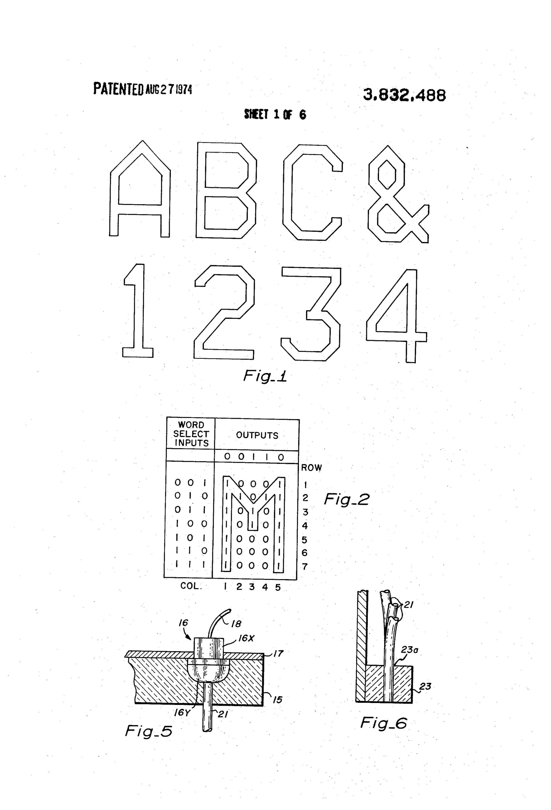
COM devices can substantially alleviate the problem of disparity in speed between computer processing and FIG. 1 is an illustration of typical characters which output data printing. However, COM devices employ may be printed with a preferred embodiment of the ing this method are expensive. present invention;
A recent development in the field has been the use 50 FIG. 2 is a chart showing the method employed for of light emitting diodes (LED) for printing alpha nu generating a character to be printed by the present in meric characters on a strip of photosensitive film. A vention;
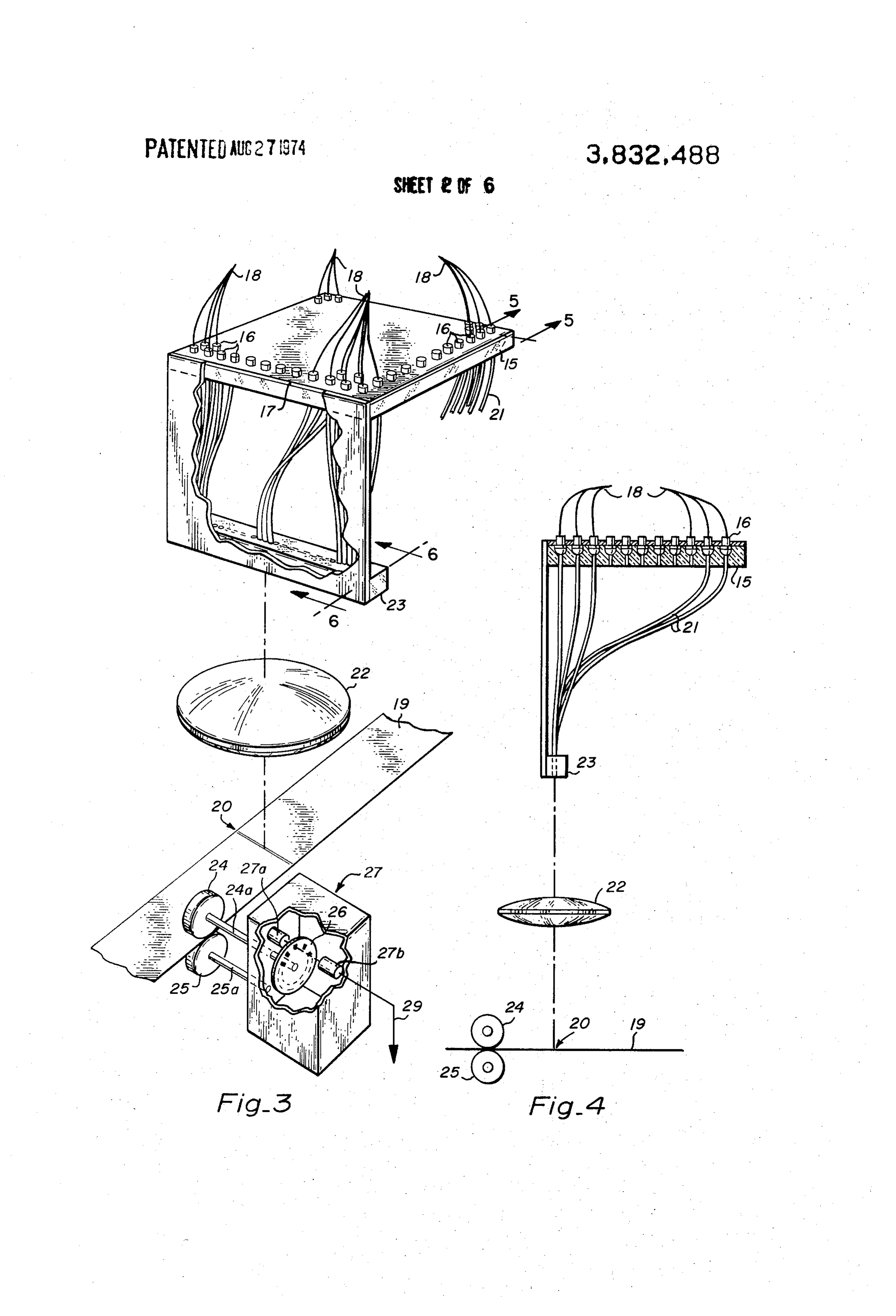
matrix of LED's is provided for each character space FIG. 3 is a perspective view of the optical compo in a line and the LED's selectively energized to form 55 nents of a COM device in accordance with the present the desired character at each position. There are two invention;
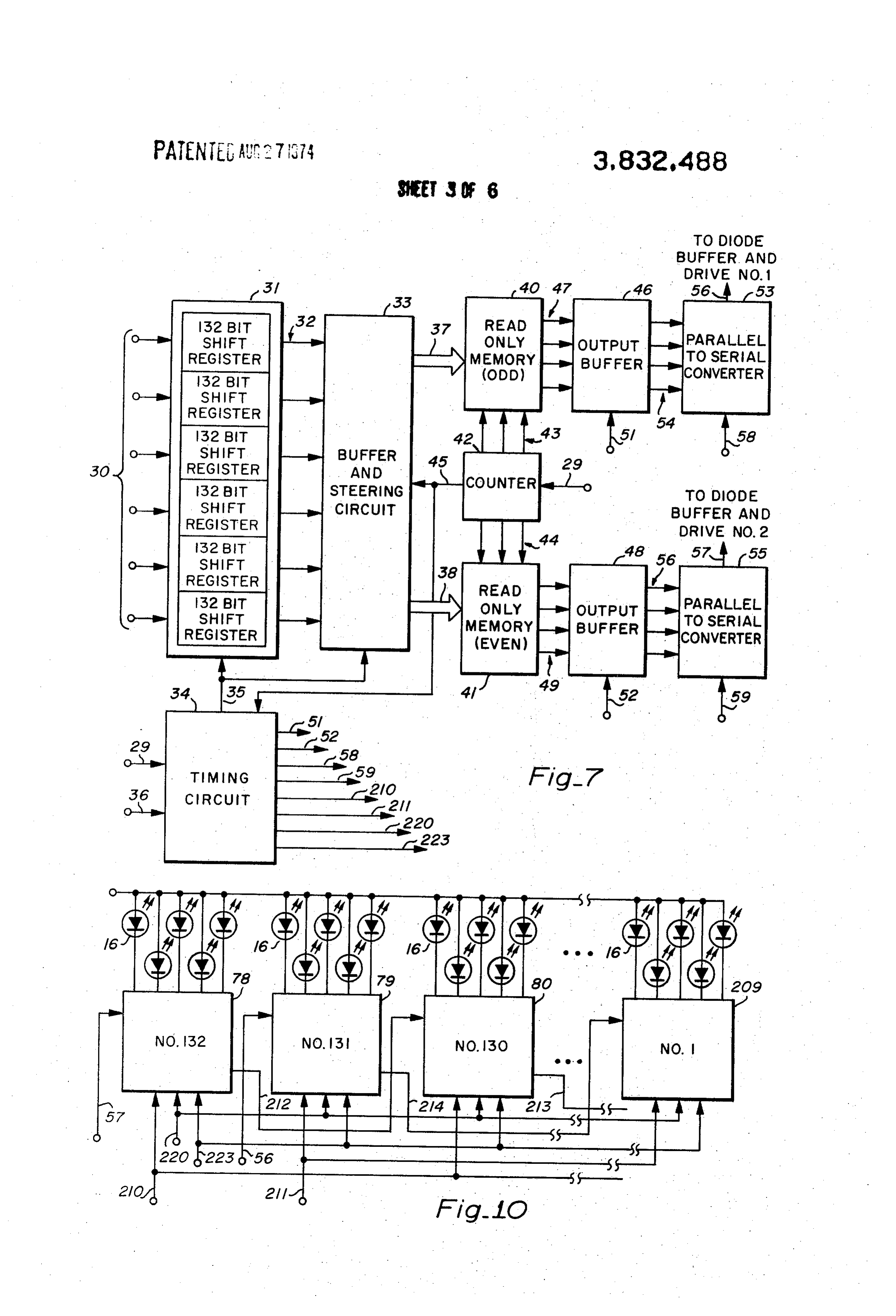
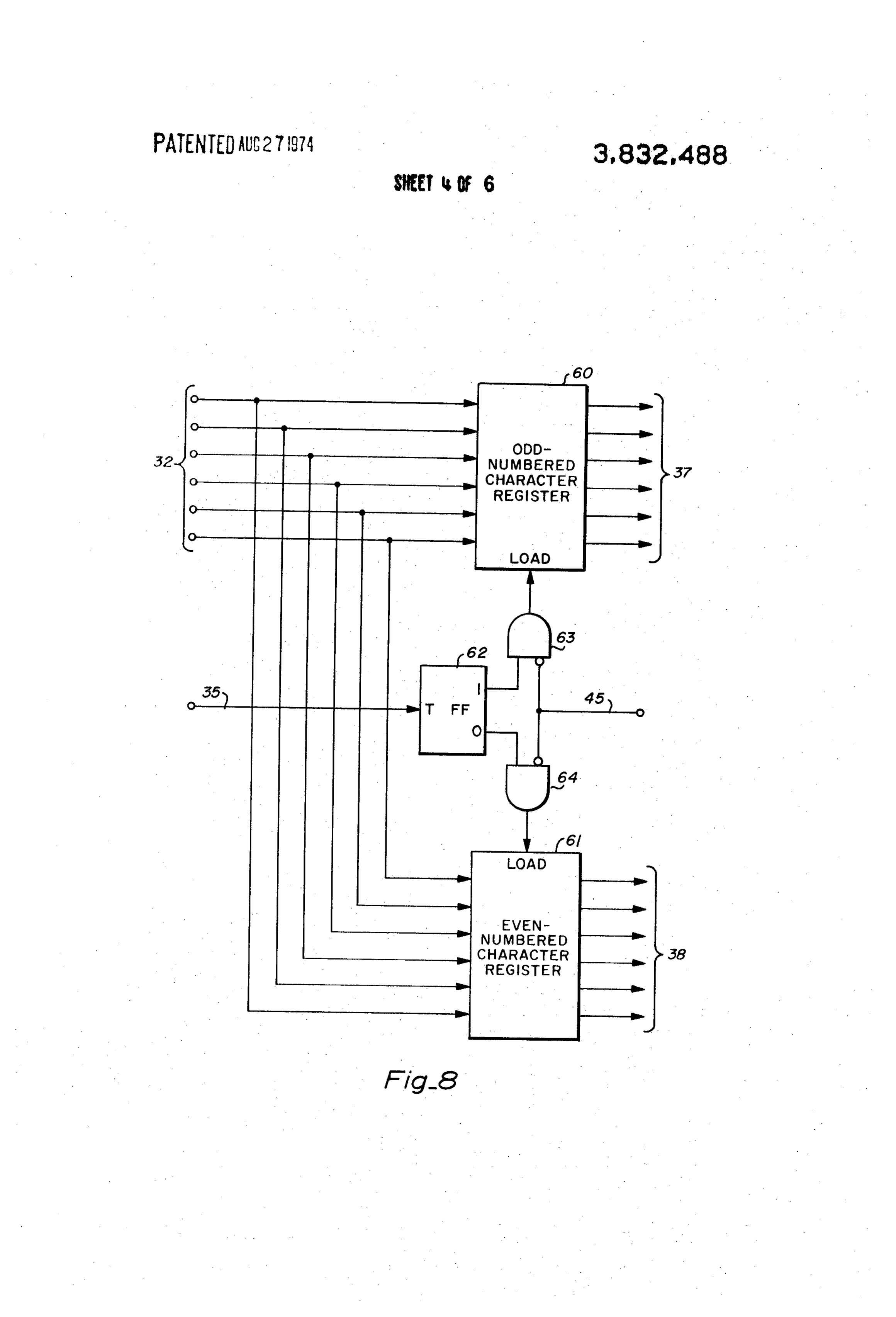
important disadvantages inherent in a system of this FIG. 4 is an elevational view, partly in section, of the type. optical components shown in FIG. 3; The first is the necessity of stopping the film at each FIG. 5 is a sectional view taken on line 5-5 of FIG. line position while the line of characters is printed. This 60 3 looking in the direction of the arrows; not only slows the printing process but also introduces FIG. 6 is a sectional view taken on line 6-6 of FIG. electrical and/or mechanical complexities into the sys 3 looking in the direction of the arrows; tem for advancing and positioning the film. FIG. 7 is a block diagram of the circuits employed for The second disadvantage flows from the large num decoding input data for printing in accordance with ber of LED's required. Each character matrix custom one embodiment of the present invention; arily consists of a 5 X 7 array or 35 diodes. For a typical 65 FIG. 8 is a block diagram of a buffer and steering cir 132 character line, a total of 4,620 LED's are required cuit constituting a portion of the block diagram of FIG. as well as circuitry for selectively energizing each ma 7;
Page 9
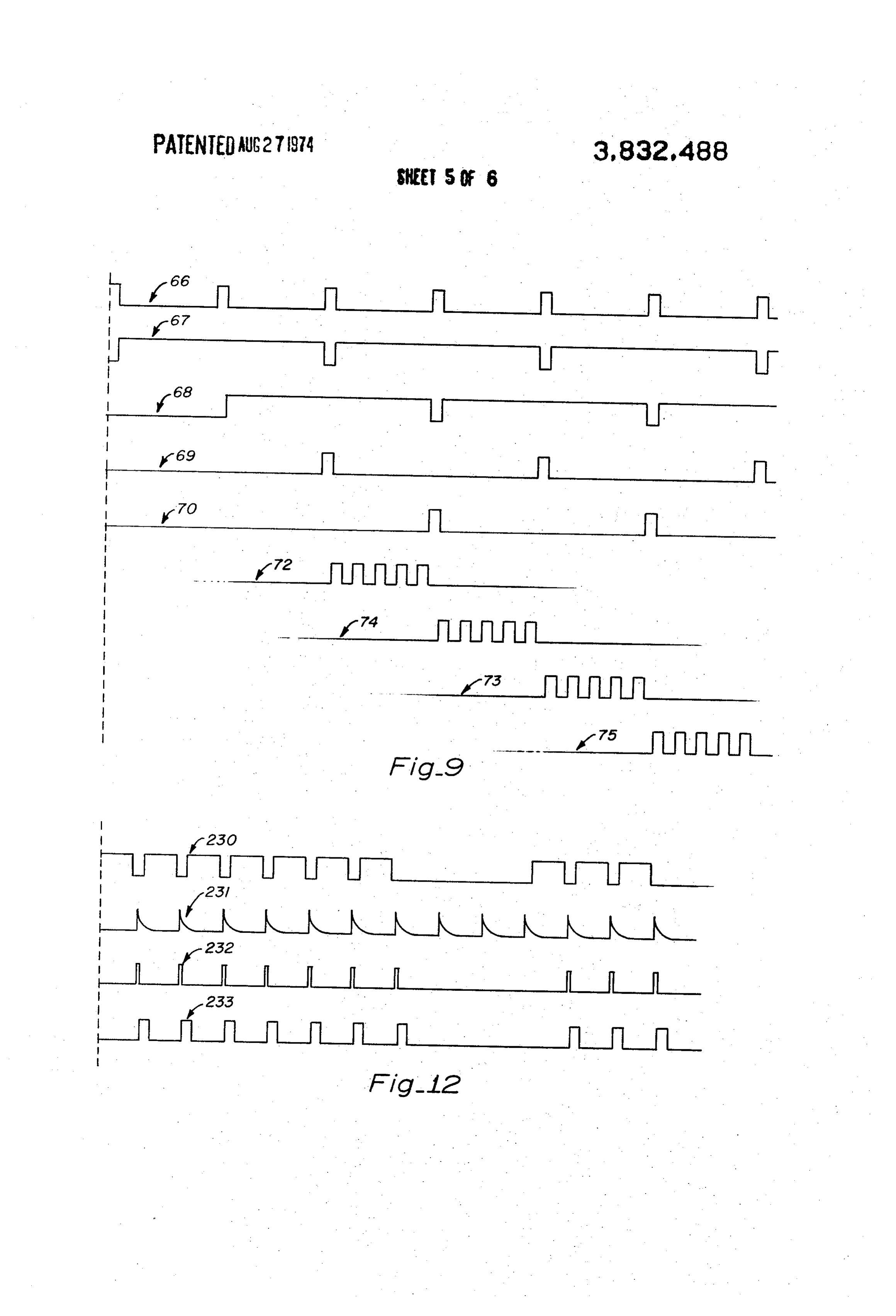
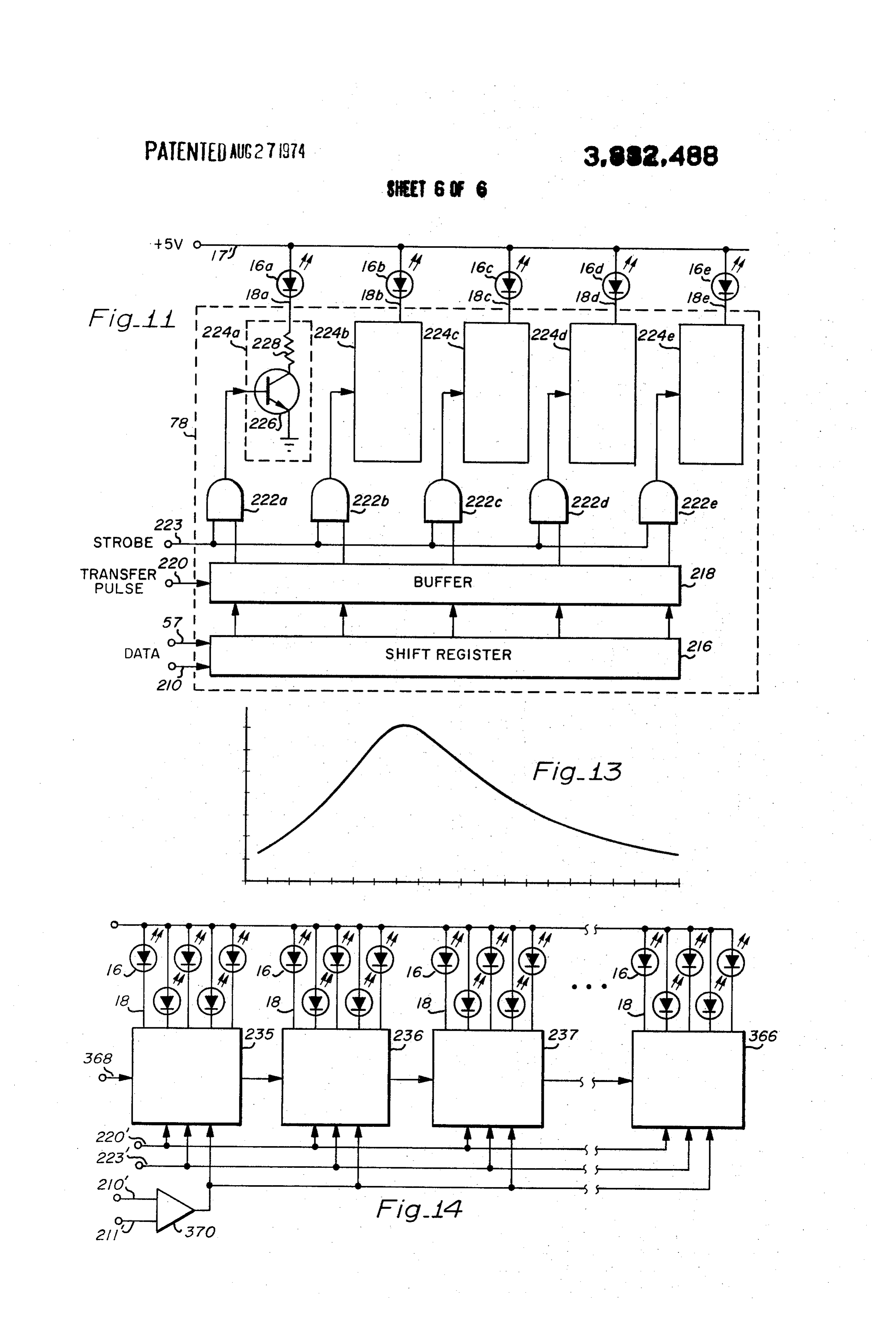
FIG. 9 is a timing diagram of the operation of decod terminal leads 18 are connected to switching circuits ing data to be printed; described hereinbelow. The diodes may be, for exam FIG. 10 is a block diagram of a typical example of the ple, model number MF1OA manufactured by Mon circuits for storing decoded data and energizing the santo Electronic Special Products, of St. Louis, Mo. light emitting diodes; These particular diodes emit light having a wavelength FIG. 11 is a detailed block diagram of an individual which is typically 6,500 Angstroms. circuit for storing data and energizing the diodes; A strip 19 of photosensitive film is moved lengthwise FIG. 12 is a timing diagram of the printing operation; in one direction by any conventional film transport mechanism (not shown). A film which was found to be
FIG. 13 is an illustration of a graph which may be () compatible with the frequency of light emitted by the printed with an alternate embodiment of the present diodes is Kodak 2479, manufactured by Eastman invention, and Kodak Company of Rochester, N.Y. As the film strip FIG. 14 is a block diagram of a plurality of circuits may be moved at a continuous rate, a simple and con for storing data and energizing the light emitting diodes ventional transport mechanism, not shown, is sufficient which is constructed in accordance with the alternate 15 for the purposes of this invention. embodiment of the present invention. Light emitted by diodes 16 in the two-dimensional DESCRIPTION OF THE PREFERRED array is directed by means of a plurality of fiber optic EMBODIMENT light guides 21 to form a linear array which is imaged to define a line of print (or portion thereof) on film 19 1. Printing Format and Technique 20 at printing station 20 extending transversely of the path Referring to the drawings and, first, in particular to of film movement. Thus, one end of each guide 2 FIG. 1, shown there are typical characters which can be abuts the lens 16Y of a respective diode 16. The other printed with one form of COM device contemplated by end of each of light guide 21 is arranged in a linear this invention, each character being formed by a com array within a support block 23, which extends trans bination of dots. A more detailed pattern of the method 25 versely of the direction of movement of the film. The employed for generating characters from a plurality of light guides may be, for example, either glass or plastic dots is illustrated in FIG. 2. Each character format is fibers manufactured by Fiber Photics, Incorporated, of subdivided into a matrix which consists of seven hori Santa Cruz, Calif.
zontal rows of five dots per row. At each position of the Travel of film 19 is monitored by a film position en matrix, a one represents the presence of a dot, and a 30 coder 27 including a pair of opposed pressure rollers 24 zero represents the absence of a dot. A single horizon and 25 disposed in frictional contact with opposite Sur tal row or slice of the character is formed at one instant faces of the film. Rollers 24, 25 are fixed to parallel of time, and each of the remaining six rows is formed shafts 24a and 25a respectively, rotatably mounted in in sequence thereafter. Therefore, each succeeding and extending into the interior of the housing of en row of dots complements the previously printed dots in 35 coder 27. Within the housing of encoder 27 is a disk 26 such a manner as to form the desired character. As will fixed to shaft 24a. Thus it will be seen that movement be shown in greater detail hereinbelow, the dots which of the film imparts rotary motion to disk 26 by way of construct the individual character format comprise a roller 24 and shaft 24a.
plurality of small points of light which impinge upon 40 Disk 26 has transparent and opaque sectors arranged photosensitive film. arcuately thereon. A light source 27a is disposed on A typical output printer device has the capability of one side of disk 26 for directing light toward the sur printing 132 characters on a single line of print, and the face of the disk. A photocell 27b is disposed on the op exemplary embodiment of the present invention to be posite side of disk 26 for receiving light from source described also has this capability. Therefore, since five 45 27a. A conductor 29 is connected to photocell 27b. Ro light sources are required for constructing one charac tation of disk 26 causes the transparent and opaque ter, then 660 (132 X5) sources of light are required per sectors to periodically interrupt light from source 27a line of 132 characters. Also, seven successive expo which in turn causes photocell 27b to supply pulses on sures are required to complete the formation of a single line 29 indicative of film movement. line of print. A space is provided between each group The vertical alignment of the components of FIG. 3 of five light sources to allow for spaces between indi 50 described hereinabove is evident from FIG. 4. Lens 22 vidual characters within a given line of print. is located between printing station 20 and support A provision is made in the circuitry for allowing verti block 23 at a point that will reduce the image of the cal spacing equivalent to three rows of dots between ends of light guides 21 to a practical size for use with successive lines of print. Therefore, ten rows are re 55 the film. A typical diameter of light guides 21 is 0.002 quired for the formation of a line of print and the corre inches and lens 22 reduces the image diameter to sponding spacing to the subsequent line of print. 0.0005 inches at the surface of the film. 3. Optics It is a well-known characteristic of flexible fiber optic FIGS. 3, 4, and 5 illustrate somewhat schematically light guides that light may be reflected therethrough the mechanical and optical aspects of the apparatus for even though the fibers may be curved. However, the generating and printing the character-forming dots. 60 intensity of the light emitted by the light guide may vary The apparatus comprises a plate 15 in which are depending on the amount of bending placed on the mounted a plurality of light emitting diodes 16 ar guide and the angle at which light is directed into the ranged in a two-dimensional array. As best seen in FIG. light guide. The light guides may be spaced a small dis 5, each LED 16 has an anode 16X, a lens 16Y., and a 65 tance from the lens to change the angle of light directed cathode terminal lead 18. An electrically conductive into the light guides. Also, the diodes may be twisted in sheet 17 on one surface of plate 15 contacts and inter their mountings to change the orientation of the light connects the anodes of all diodes 16. Individual cathod received by the light guides. Once the intensity of the
Page 10
S 6 light is adjusted in this manner, no additional adjust A provision is made for cutting operation time in half ments are required. The intensity of the light emitted by decoding all odd-numbered characters in one por by the diode may be varied in the switching circuit tion of the circuit, and decoding all even-numbered components to be described hereinbelow. characters in an identical second portion of the circuit. FIG. 6 is a cross-sectional view of support block 23 The term "odd-numbered characters' as used herein and shows the light guides mounted therein. An open denotes characters in positions 1, 3, 5, 7, etc., of the ing such as 23a is provided in block 23 for receiving line of 132 characters to be printed. Likewise "even each of light guides 21. The primary function of block numbered characters' denotes characters in positions 23 is to arrange the ends of the light guides in a linear 2, 4, 6, 8, etc., of the line of 132 characters to be array and in a position which directs light in a direction 10 printed. Timing signals on line 35 to circuit 33 control which is perpendicular to the film surface. the steering of odd-numbered characters on lines 37 In operation, selected ones of diodes 16 are ener and even-numbered characters on lines 38. Lines 37 gized via their respective conductors 18 and light gen are connected as an address input to a read only mem erated passes through the respective diode lens 16Y. ory (ROM) 40 and lines 38 are likewise supplied as an This light is conducted through the corresponding light 15 address input to a ROM 41. Read only memories 40 guides 21 and reflected from the end of the light guides and 41 may be, for example, Model No. EA3501 manu mounted within support block 23. Lens 22 forms a re factured by Electronic Arrays, Inc., of Mountain View, duced image of the linear array of light guide ends onto Calif. A typical application for the EA3501 is the gen film 19 which is thus exposed to make a latent photo eration of characters by subdividing each character graphic image of each light guide end which appear as 20 into seven horizontal rows. An address representative dots when the film is developed. of the character is supplied as one set of inputs, and Reverting to FIG. 2, row 1 is first aligned at print sta row-count signals from a counter are supplied as a sec tion 20 for exposure, and diodes 16 corresponding to ond set of inputs. Therefore, seven sets of binary num columns 1 and 5 are energized. When row 2 is aligned bers, which correspond to the rows, are supplied se at print station 20 for exposure, the diodes correspond 25 quentially from the ROM in response to a single char ing to columns 1, 2, 4 and 5 are energized. The film acter address input and a series of row-count signals continues to pass through print station 20 for the subse from the counter.
quent rows, and additional exposures are made on the This particular type of ROM operates with ASCII bi film until the full complement of dots for the character nary codes as an address input; therefore, input data on has been exposed. While described with respect to a 30 lines 30 should conform to this code. However, other single character, it will be understood that an entire types of ROM's may be used which operate with other line, e.g., 132 characters may be printed at the same types of binary codes.
time. Therefore, the first row of all 132 characters may Counter 42 is incremented by pulses on line 29 from be exposed simultaneously (or in a ripple fashion), then encoder 27. Counter 42 supplies a count of one row 2 for all 132 characters may likewise be exposed, 35 through seven to ROM 40 via lines 43, and also etc.; until seven rows of all 132 characters are exposed. supplies the same count sequence to ROM 41 via lines 4. Circuits 44. Also, a signal is supplied from counter 42 to circuits 33 and 34 on line 45, which is indicative of a count of
Referring now to FIG. 7, six-bit binary data is sup 40 8, 9 and 10. This signal is employed within circuits 33 plied on lines 30 from a data source such as a digital and 34 to allow for the vertical spacing between indi computer (not shown); each combination of 6 bits cor vidual lines of print.
responds to a binary code for a character to be printed. The binary numbers for individual rows of a particu These lines supply input data to six shift registers 31 lar character are supplied to output buffer 46 from which are capable of storing 132 bits each. The shift 45 ROM 40 via lines 47, and to buffer 48 from ROM 41 registers may be constructed in a manner as shown on via lines 49. A timing signal is supplied to buffer 46 via page 346 of the book entitled: "Pulse, Digital, and lines 51, and to buffer 48 via line 52. These timing sig Switching Waveforms," by J. Millman and H. Taub. nals control the loading of these buffers with the binary The binary codes, representative of characters to be numbers from the ROM's. It is pointed out at this junc printed, are supplied from registers 31 via lines 32 to ture that data (binary numbers) on lines 47 and 49 are a buffer and steering circuit 33. A timing circuit 34 pro 50 indicative of a single horizontal slice of an individual vides timing signals to registers 31 and circuit 33 via character to be printed, whereas data on lines 37 and line 35 for synchronization of operation. It is pointed 38 is the ASCII binary code indicative of the complete out at this juncture that a provision is made within reg individual character itself. Data is supplied to parallel isters 31 to re-cycle the data stored therein seven times 55 to-serial converter 53 from buffer 46 via lines 54. Like for the seven horizontal rows of the characters to be wise, data is supplied to parallel-to-serial converter 55 printed. Conventional gating techniques are employed from buffer 48 via lines 56. Serialized data is supplied which are responsive to timing signals from circuit 34. from converter 53 on line 56 and from converter 55 on The timing circuit is synchronized by the driving equip line 57. A timing signal is supplied to converter 53 on ment, such as the data source, by signals supplied on line 58 and to converter 55 on line 59 for transferring line 36. Also, pulses on line 29 are supplied to the tim 60 the data received from the buffers in serialized form on ing circuit to synchronize the film movement to the cir lines 56 and 57, respectively.
cuits. The signals from timing circuit 34 to registers 31 FIG. 8 illustrates buffer and steering circuit 33 in control the loading of the registers. Timing diagrams more detail. The six data lines 32 from shift registers 31 will be discussed hereinbelow which will illustrate the 65 are connected, in parallel, to odd register 60 and even relationship of the numerous signals provided by circuit register 61. Line 35 is connected to the toggle input of 34. Timing circuits are well-known to those conversant a flip-flop 62. The "one" output of flip-flop 62 is con with the art. nected to one of two inputs of AND gate 63. The sec
Page 11
ond input of AND gate 63, which is an inverting input, acters by ROM 41. Waveform 69 represents the timing is connected to line 45. The "Zero' output of flip-flop signal supplied on line 51 for loading data from ROM 62 is connected to one of two inputs of AND gate 64. 40 into buffer 46, and waveform 70 represents the tim The second input of AND gate 64, which is also an in ing signal supplied on line 52 for loading data from verting input, is connected to line 45. The output of 5 ROM 41 into buffer 48. Waveforms 72 and 73 repre AND gate 63 is connected to a "load' input of register sent the pulses supplied on line 58 for transferring data 60, and the output of AND gate 64 is connected to the serially from converter 53, and waveforms 74 and 75 "load' input of register 61. The output of register 60 represent the pulses supplied on line 59 for transferring is connected to lines 37, and the output of register 61 data (again serially) from converter 55. This decoding is connected to lines 38. 10 operation of row one continues through the first row of in operation, the binary code for the first character all l32 characters.
to be printed is applied to the inputs of registers 60 and As shown in FIG, 10, four of 132 storing and diode 61. A pulse is supplied on line 35 which sets flip-flop switching circuits 78-209 are illustrated with electrical 62, and the "one' output thereof supplies a high-level connections therebetween. Circuit 78 controls the signal to AND gate 63. Assume that counter 42 is at a 15 switching of the five diodes associated with character count of one. Therefore, the signal on line 45 is at a low position number 132, and circuit 209 controls the level. Since the second input to AND gate 63 is an in switching of the five diodes associated with character verting input, a high-level signal appears at the "load' position number one. The serialized form of the binary input of register 60. The binary code on lines 32 is now numbers from converter 53 (odd-numbered charac entered into register 60 and appears at the output ters) is supplied to circuit 79 via line 56, and the serial thereof on lines 37. The binary code applied to register ized form of the binary numbers from converter 55 61 had no effect since AND gate 64 was not enabled. (even-numbered characters) is supplied to circuit 78 The next pulse supplied on line 35, which indicates the via line 57. Each of circuits 78-209 contains a shift reg presence on lines 32 of the binary code for the second ister constructed in the same fashion as that described character to be printed, changes the state of flip-flop 25 hereinabove for registers 31. A shift pulse is supplied 62. Therefore, AND gate 64 is enabled and the second to all the circuits for even-numbered characters on line binary code is loaded into register 61. This process con 210, and to all the circuits for odd-numbered charac tinues through row one for all 132 characters, then ters on line 211. These shift pulses are produced within counter 42 increments to a count of two and the same timing circuit 34 of FIG. 7. 132 binary codes are applied to registers 60 and 61 in 30 The shift registers contained within the circuits for the same fashion. When the binary code for the 132 the odd-numbered characters are connected in one se characters has been applied on lines 32 seven times ries chain, and the registers contained within the cir (seven horizontal rows of the characters to be printed), cuits for the even-numbered characters are connected a count of 8, 9 and 10 from counter 42 inhibits the in a second series chain, i.e., the output of the register loading of data into registers 60 and 61 via the inverting 35 in circuit 78 is connected to the input of the register in inputs to AND gates 63 and 64. More particularly, circuit 80 via line 212, and the output of the register in when counter 42 is at a count of eight, nine or 10, a circuit 80 is connected to register in the next circuit high-level signal appears on line 45 which disables (not shown) via line 213. Likewise, the output of the AND gates 63 and 64. As was discussed hereinabove, 40 register in circuit 79 is connected to the input of the the count of eight, nine and i () allows for the vertical register in the next circuit (not shown) via line 214. spacing between individual lines of print. Also, during The operation of the circuits in FIG. 10 will be more the time allowed for vertical spacing, new data is readily understood following a detailed description of loaded into registers 31 from the data source. the structure of a typical storing and switching circuit. Referring again to FIG. 7, the first binary code is Sup 45 FIG. 11 is a block diagram of storing and switching cir plied to ROM 40 on lines 37. Assume once again that cuit 78. Line 57, which supplies serialized data from counter 42 is at a count of one. Therefore, ROM 40 is converter 55, is connected as an input to shift register addressed to decode a binary number representative of 216. Shift pulses are supplied to the shift register on the first horizontal row of the first character. This bi line 210 as stated hereinabove. Register 216 has the ca nary number is transferred to output buffer 46 via lines SO pability of storing the five-bit binary number which cor 47 when a "load" pulse is supplied on line 51. Once the responds to the 5 bits for an individual row of a given binary number is loaded in buffer 46, it is then applied character to be printed. The binary number stored in to converter 53 via lines 54. A series of pulses are sup register 216 is supplied, in parallel, to buffer 218; and plied on line 58 which transfer the binary number, seri this number is transferred to the buffer upon the appli ally, on line 56 to the print circuitry. In a similar man 55 cation of a transfer pulse on line 220 from timing cir ner, the binary number for the second row is decoded cuit 34. The binary number which is now stored in from ROM 41 and is transferred to buffer 48 and con buffer 218 is supplied to one of two inputs of AND verter 55. gates 222a through 222e, the second inputs of which The operation of the circuits shown in FIGS. 7 and are connected to a line 223 supplying a print strobe sig 8 will be more fully understood from a description of 60 nal from timing circuit 34. Respective switching cir the timing diagram shown in FIG.9. Waveform 66 rep cuits 224a-224e are provided between the outputs of resents the transfer of a series of characters from shift gates 222a-222e and LED's 16a-16e. As previously de registers 31 to circuit 33, wherein each positive pulse scribed, the anodes of LED's 16a-16e are intercon is indicative of the time required for transferring a sin nected by a metal sheet 17 (FIGS 3-4), represented in gle character binary code. Waveform 67 represents the 65 FIG. 11 by conductor 17', to which is applied a positive decoding operation of odd-numbered characters into potential of low magnitude, e.g., 5V.
horizontal rows by ROM 40, and waveform 68 repre As switching circuits 224a–224e are duplicative, only sents the decoding operation of even-numbered char one, 224a, is shown and will be described. Thus, 224a
Page 12
consists of an NPN transistor 226, the base terminal of transfer pulse (waveform 232) is applied on line 220 which serves as the input and is connected to the out put of gate 222a. The emitter of transistor 226 is The numberthe whereupon
number is transferred to buffer 218.
applied as inputs to one side of AND grounded and the collector is connected through a se gates 222a through 222e.
ries resistor 228 to the cathode terminal 8a of LED 5 (waveform 233) is appliedWhen on a print strobe signal line 223, AND gates 16a. Switching circuits 224b-224e are similarly con 222a and 222e apply a high-level signal nected between the outputs of gates 222b-224e at the circuits 224a and 224e, respectively. Thistocauses switching cur cathode terminals 18b-18e of LED's 16b-16e.
Referring again to FIG. 10, lines 220 and 223 are emitted from these two diodes. Since a low level signalis rent to pass through diodes 6a and 16e and light connected to each of circuits 78-209, respectively. The O is applied to the inputs of AND gates 222b, 222c and binary numbers representative of the first row of the even-numbered characters are supplied serially, with 222d, diodes 16b, 16c and 16d are not effected. As mentioned hereinabove, a provision is made the lowest position number first, to circuit 78 via line within 57. Pulses on line 210 shift the binary numbers through the 132registers 31 for recycling the binary codes for characters back into the individual registers.
a register (not shown), which is similar to register 216, 15 Therefore, upon completion of row one decoding for within each of the circuits 78,80, 82, etc. At the same all 132 characters, the operation of decoding row two time, the binary numbers representative of the first row for the same 132 characters commences. When the of the odd-numbered characters are supplied serially, film has moved to a position corresponding to the sec again with the lowest position number first, to circuit 79 via line 56. Pulses on line 211 shift the binary num 20 ond row of the characters to be printed, a signal is sup bers through registers (not shown) within circuits 79, plied on line 29 (waveform 231) from encoder 27 to 8, etc. step counter 42 to a count of two. When the code When the serialized form of the binary numbers rep 001 101 for the letter M in character position 132 is ap resentative of the first row of 132 characters for a given plied as an address input to ROM 41 for a second time, line of print are loaded into the shift registers within 25 and counter 42 is at a count of two (Ol O), then the bi circuits 78-209, a transfer pulse is supplied on line 220. nary number 11011 is supplied to buffer 48 from ROM This transfers the binary numbers to the corresponding 41. This binary number is transferred serially from con buffers whereupon a print strobe signal is supplied on verter 55 to shift register 216. When a transfer pulse line 223 which enables the AND gates. A typical AND (waveform 232) is again supplied on line 220, the bi gate 222a provides a high-level signal to a typical NPN 30 nary number is transferred to buffer 218. In a similar transistor 226 which renders the transistor conductive manner, diodes 16a, 16b, 16d and 16e are switched on enabling current flow from the 5V source, through con by the application of high-level signals from AND gates ductor 17, diode 16a, resistor 228, to ground causing 222a, 222b, 222d and 222e to circuits 224a, 224b, 224d light to be emitted from diode 16a. The brightness of and 224e, respectively. This process continues until all the light emitted from the LED is determined by the 35 plete.seven rows of the characters to be printed are com value of regulating resistor 228. The remaining LED switching circuits operate in a similar fashion. A SECOND EMBODIMENT OF THE PRESENT The timing diagram shown in FIG. 12 illustrates a INVENTION complete cycle of circut operation for printing a line of 40 characters and allowing for vertical spacing to the sub It is also possible with the concept of this invention, sequent line. Waveform 230 represents the decoding to construct a linear array of adjacent light sources operation for a single line of print and the correspond within support block 23 for printing graphical output ing vertical spacing thereafter. Each of the positive data, such as that shown in FIG. 13. By employing the pulses represents a single decoding operation for an in 45 same technique as disclosed herein, the graph is subdi dividual row of a given line of characters to be printed. vided into individual horizontal rows, and a combina Waveform 231 represents the pulses supplied from en tion of dots are exposed on the film for each row in se coder 27 on line 29. Each positive pulse represents a quence. Any image which may be represented by the single row. Waveform 232 represents the transfer pulse well-known CRT raster-scan display technique can also supplied on line 220. Waveform 233 represents the 50 be printed by a device in accordance with the present print strobe supplied on line 223. invention. Each raster is supplied sequentially as an in Referring again to FIG. 2, the binary number 001101 put, wherein the raster corresponds to a row and indi is the ASCII code for the letter M. As described herein vidual elements of the raster correspond to the dots. above, each character to be printed is subdivided into As shown in FIG. 14, a group of storing and switching seven rows of 5 bits per row. The binary numbers in the 55 circuits 235-366, which are constructed in the same column designated (word select inputs) represent the manner as that shown in FIG. 10, are connected in a row-count signals supplied to ROM 41 via lines 44 from single series chain. Serialized binary data, which repre counter 42. Assume, for example, that binary number sents a single raster of the graph or drawing to be 00 101 was character number 132, an even-numbered printed, is supplied from a data source to circuits character, to be printed on a given line of print. This 60 235-366 on line 368. Lines 210' and 211" are con binary number is applied as an address input to ROM nected to the two inputs of an OR gate 370. The output 41 via lines 38. Counter 42 applies a count of one of the OR gate is connected to the shift input of each (001) to ROM 41 via lines 44. The output binary num of the shift registers contained within circuits 235-366. ber from ROM 41 is 10001, and is transferred subse Transfer pulses are supplied on line 220', and print quently to buffer 48 and converter 55. The converter strobes are supplied on line 223'.
transfers this binary number serially to storing and 65 The operation is essentially the same as described switching circuit 78 via line 57. This binary number is shifted into register 216 and stored therein until a hereinabove for the circuit shown in FIG, 10. The pri mary difference is that serialized data is supplied to the
Page 13
storing and switching circuits directly from the data that a plurality of rows of said selected exposed SOCC. areas are at spaced intervals with each other and For example, if a drawing or graph were represented when viewed together display data in a desired for by the conventional CRT technique, then a single ras hat.
ter of the CRT image is loaded into all of the diode 5 cording 2. Apparatus as defined in claim 1 wherein said re buffer and driver units. The switching of diodes 16 is medium is film.
effected in the same manner as described hereinabove. 3. Apparatus as defined in claim 1 wherein said light sources are light emitting diodes.
If several diodes are energized at a given time, then directing4. Apparatus as defined in claim 1 wherein said light means further comprises a lens disposed be a large current drain would be demanded from the 10 tween said light guides and the recording medium pro power supply. Therefore, an alternate technique of jecting a reduced image of the row image onto said re supplying separate print strobes individually to circuits cording medium.
235-366 may be employed which would mitigate this 5. Apparatus as defined in claim 4 which includes an problem. One such circuit modification may be, for ex encoder physically coupled to said recording medium ample, the insertion of a time delay network between 15 for producing pulses indicative of increments of re cording medium movement to synchronize said ener line 223 from circuit 34 and the shift pulse inputs to the gizing registers within circuits 235-366. The time delay net means with said moving means. work contemplated herein is responsive to a single line6. ofThe invention according to claim 5 wherein said information comprises M alphanumeric charac pulse input, and has a provision for a plurality of indi ters each formed from a matrix of x rows and y columns vidual outputs wherein each output provides a pulse 20 of dots, said which is delayed in time from the pulse on a second times y, said plurality of light sources is equal to M light directing means images said light output. Therefore, each of circuits 235-366 responds sources in groups of y and said means to energize is op independently to individual print strobes or in a ripple erated x successive times to thereby print a line of al fashion which was alluded to hereinabove. A delay net phanumeric characters.
work such as this is well-known in the art and may be 25 7. The invention according to claim 6 wherein said M constructed from a counter and decoders or simply a alphanumeric characters are provided as coded binary time delay line. inputs and further including means to decode said in While the invention has been described with respect puts the into x successive sets of said data inputs defining dots to be recorded on said x successive rows.
to a preferred and second embodiment, it will be appar ent to those skilled in the art that various improvements 30 on8.aApparatus to record information, a line at a time, photosensitive medium by selectively exposing and modifications may be made without departing from spaced areas which are transversely aligned with re the scope and spirit of the invention. Accordingly, it is spect to the axis of advance of that medium, as such to be understood that the invention is not to be limited medium is advanced to form successive and substan by the specific illustrative embodiments, but only by 35 tially parallel rows of said selectively exposed areas, the scope of the appended claims. which rows, when viewed together, combine to pro What is claimed is: duce said information, comprising: 1. Apparatus to record information, a line at a time, a plurality of fiber optic light guides, a first end of on a photosensitive medium by selectively exposing each of said light guides arranged such that said spaced areas which are transversely aligned with re first ends form a row, spect to the axis of advance of that medium, as such a plurality of light sources, equal in number to the medium is advanced, to form successive and Substan number of light guides, and one of said plurality of tially parallel rows of said selectively exposed areas, light sources adjacent the second end of each of which rows, when viewed together, combine to pro said light guides such that light from each of said light sources is transmitted through the light guide duce said information, comprising: with which it is adjacent, and such that said trans a plurality of fiber optic light guides, a first end of 45 mitted light is projected from said first end of that each of said light guides arranged such that said light guide which is in a row with the first ends of first ends form a row; the other light guides;
a plurality of light sources, equal in number to the said photosensitive recording medium positioned to number of light guides, and one of said plurality of intercept light projected from said first ends of said light sources adjacent the second end of each of 50 R ight;
of light guides for recording said projected said light guides such that light from each of Said a lens disposed between said row of first ends and the light sources is transmitted through the light guide recording medium for reducing the image of said with which it is adjacent, and such that said trans light projected from said first ends; mitted light is projected from said first end of that SS control means responsive to data inputs for selec light guide which is in a row with the first ends of tively energizing said light sources such that light is the other light guides; Elected from selected ones of said row of first said photosensitive recording medium positioned to endS, intercept light projected from said first ends of said an encoder physically coupled to said recording me row of light guides for recording said projected 60 dium for producing pulses indicative of medium light; movement, and control means responsive to data inputs for selec driving means responsive to said encoder pulses and tively energizing said light sources such that light is synchronized with said control means for moving projected from selected ones of said row of first said medium in a direction substantially perpendic ends; and ular to said row of light guide ends such that a plu driving means synchronized with said control means 65 rality of rows of said selected exposed areas are at for moving said medium in a direction substantially spaced intervals with each other and when viewed together display*k data ink a desired format.
perpendicular to said row of light guide ends such ck k k
Provenance
- Collection
- Cited prior art
- Original PDF
- patentimages.storage.googleapis.com →
- Filed
- 1972-06-29
- Pages
- 13
- Method
- pdftotext (the PDF's own text layer) + pdftoppm 300dpi page scans
- Source
- Google Patents bibliographic record
- Granted
- 1974-08-27
- Inventors
- W Fahey; R Johnson; Singer Co
- Transcribed from
- patentimages.storage.googleapis.com →