patent · US3652855
Radiation image amplifier and display comprising a fiber optic matrix for detecting and coding the radiation image pattern
28 March 1972
Page 1 — bibliographic record
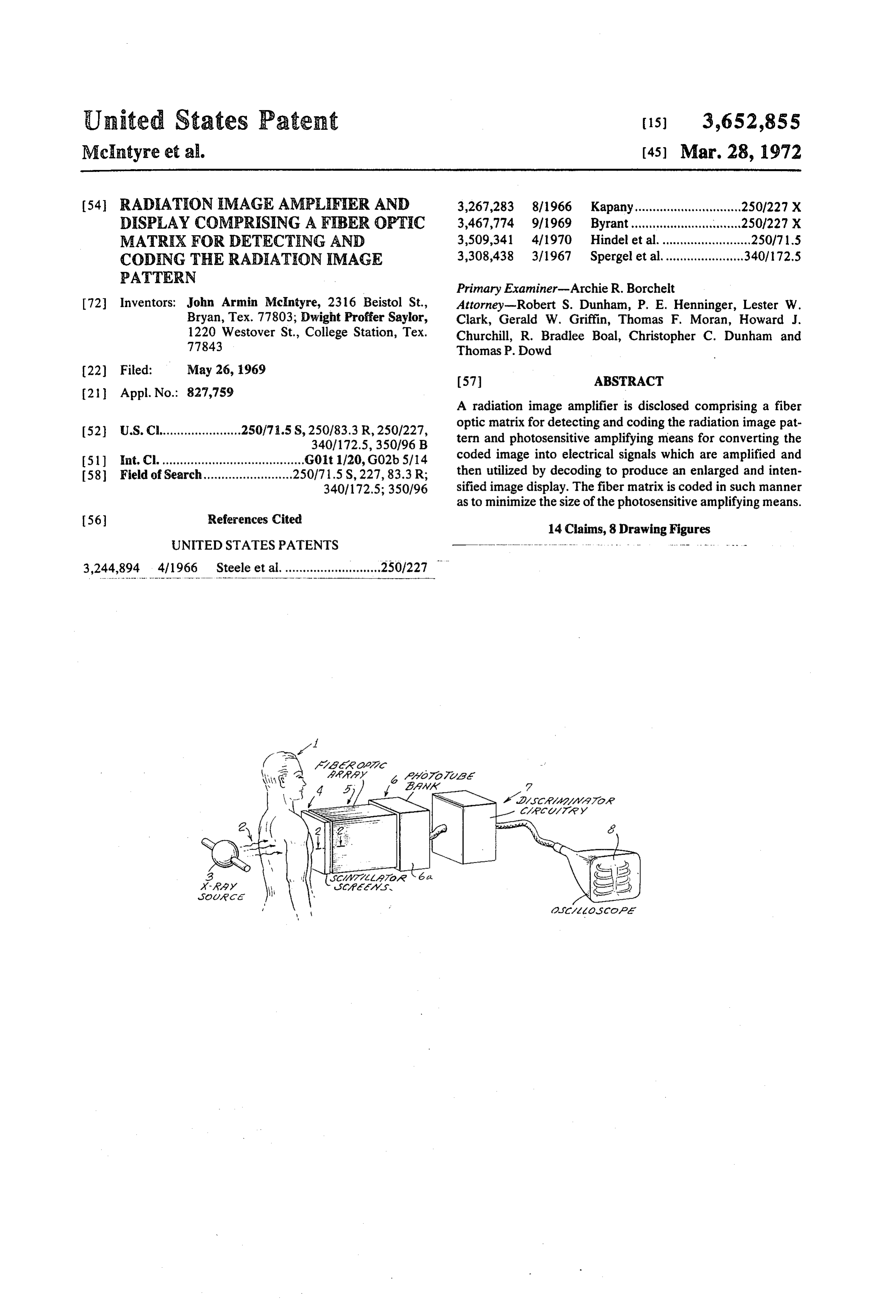
United States Pater at (15) 3,652,855 McIntyre et al. (45) Mar. 28, 1972 54 RADATION MAGE AMPLEFEER AND 3,267,283 8/1966 Kapany.............................. 250/227 X DISPLAY COMPRISING AFBER OPTC 3,467,774 9/1969 Byrant....................... ........250/227 X MATRIX FOR DETECTING AND 3,509,341 4/1970 Hindel et al........................., 250/715 CODENG THE RADHATION MAGE 3,308,438 3/1967 Spergel et al....................... 340,172.5
PATTERN
Primary Examiner-Archie R. Borchelt 72 Inventors: John Armin McIntyre, 2316 Beistol St., Attorney-Robert S. Dunham, P. E. Henninger, Lester W. Bryan, Tex. 77803; Dwight Proffer Saylor, Clark, Gerald W. Griffin, Thomas F. Moran, Howard J. 1220 Westover St., College Station, Tex. Churchill, R. Bradlee Boal, Christopher C. Dunham and 77843 Thomas P. Dowd
A radiation image amplifier is disclosed comprising a fiber 52) U.S.C.......................250/7.5S, 250/83.3 R,250/227, optic matrix for detecting and coding the radiation image pat 340/172.5, 350/96 B tern and photosensitive amplifying means for converting the 51) int. Cl. ........................................ G01t 1120, G02b 5/14 coded image into electrical signals which are amplified and 58 Field of Search......................... 250/71.5S, 227, 83.3 R; then utilized by decoding to produce an enlarged and inten 340/172.5; 350/96 sified image display. The fiber matrix is coded in such manner as to minimize the size of the photosensitive amplifying means.
14 Claims, 8 Drawing Figures
UNITED STATES PATENTS
3,244,894 4/1966 Steele et al..........................250/227
Soeaga (2 cago scoaa.
Page 2
Drawing sheet — no readable text.
Page 3
PATENTED MAR 28 1972 3, S52,855
Fig. E.
6%/-/fay Za/va N. W 4:22ar soe/Meat 47 A43
ea/2a2-Pa i E. INVENTOR.
oAw Ave/unres
assa
Page 4
Drawing sheet — no readable text.
Page 5
RADATION MAGE AMPELFER AND DISPLAY BRIEF DESCRIPTION OF THE DRAWINGS
COMPRISINGA FBER (OPTIC MATRX FOR
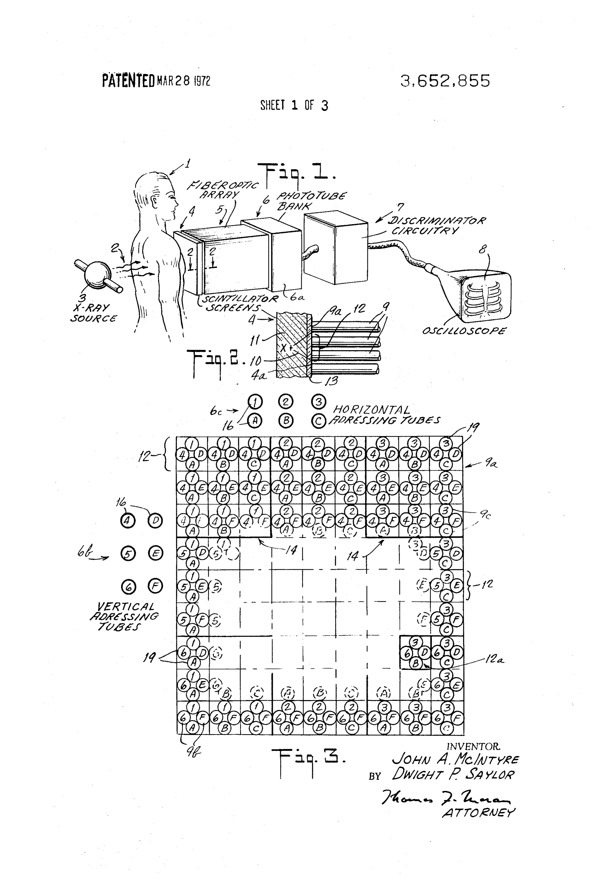
DETECTING AND CODNG THE RADATION MAGE FIG. is a diagrammatic view of the system of the present PATTERN invention being used in combination with a diagnostic X-ray apparatus;
BACKGROUND OF THE INVENTION FIG. 2 is an enlarged view of a portion of the system shown The present invention relates to the field of electronic in FIG. 1, illustrating the image-detecting fiber array picking image display and more particularly to a system for detecting up a light signal from a scintillation screen; FIG. 3 is a diagrammatic view illustrating the matrixing ar and electronically amplifying radiation images utilizing fiber 10 rangement for connecting the fibers to the photomultiplier optic coding.
It has long been a problem in both the photographic and tube array;
electronic image-producing art to detect small weak images 3 intendedistoaachieve
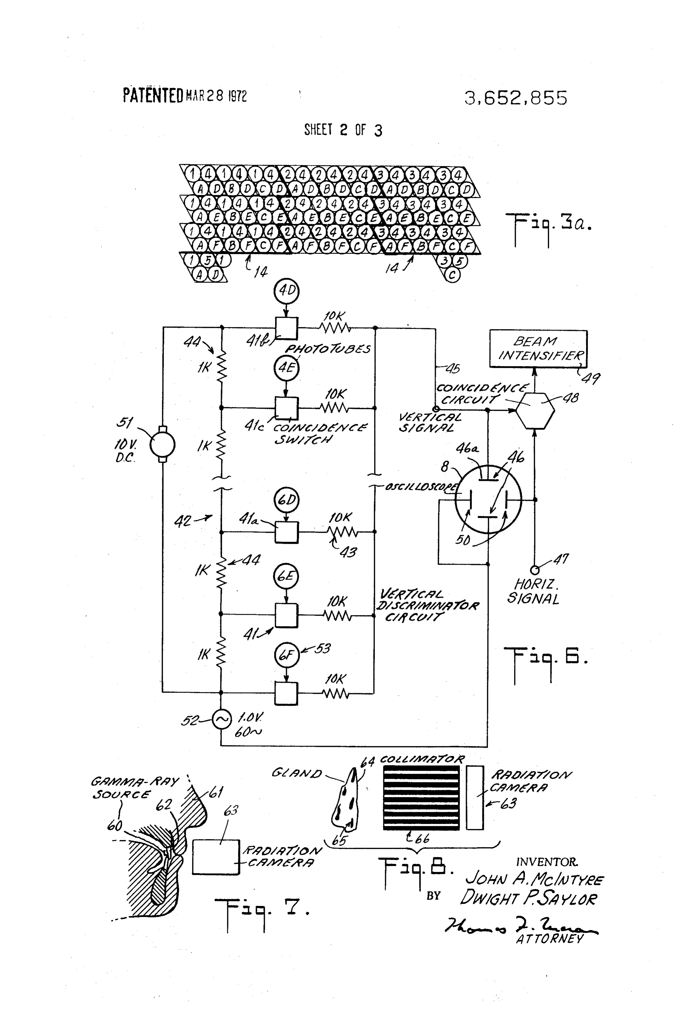
FIG.3a modification of the arrangement shown in FIG.
improved image resolution;
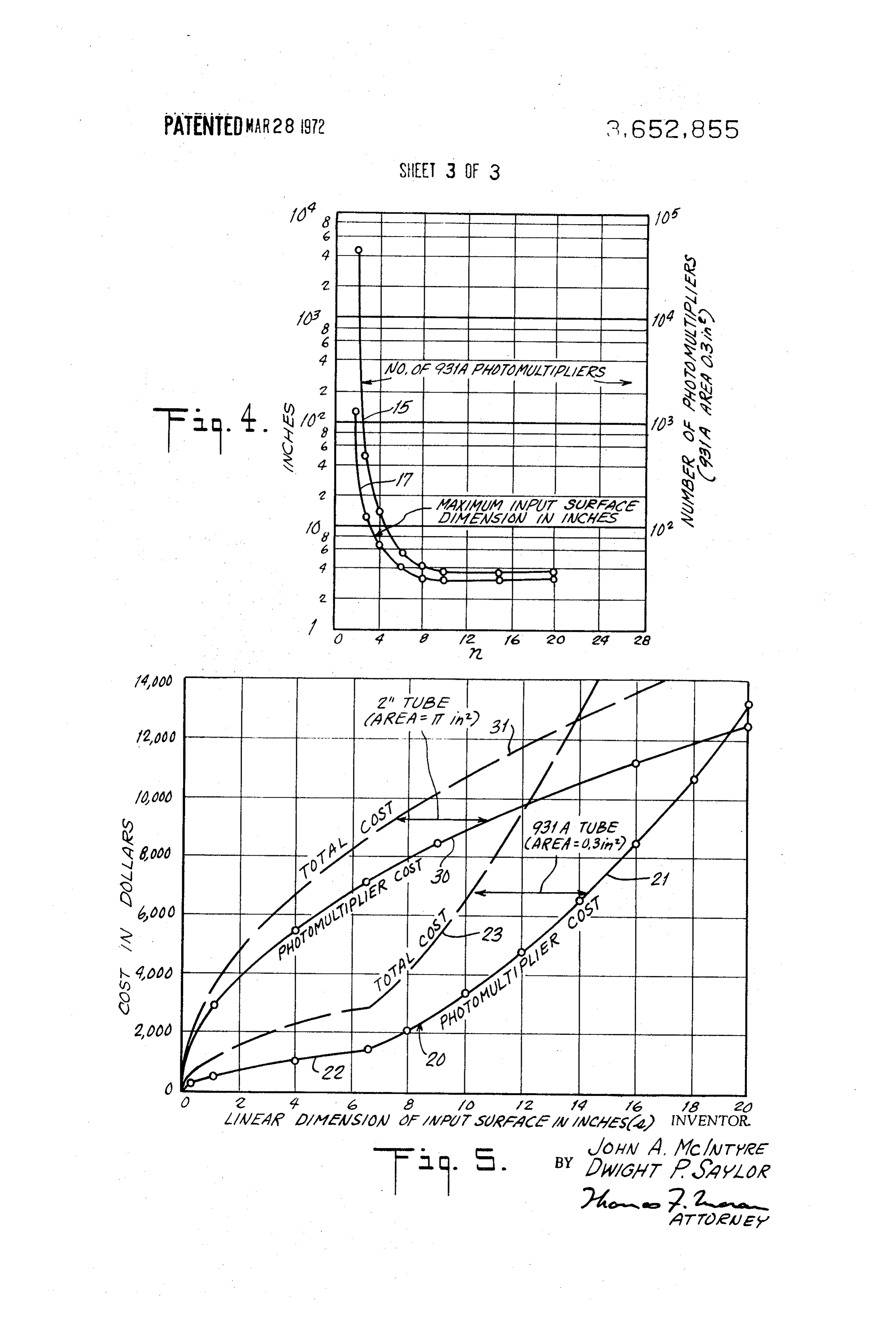
and reproduce them in enlarged intensified form. Various electronic devices have been developed, such as television 15 tiveFIG. 4 is a plot showing the size of the input or photosensi surface and the number of photomultipliers required as a cameras and image intensifier tubes which accomplish this function of the number offibers in a unit area of input surface; end to some degree. However, while the television camera can give output pictures of sufficient size and brightness, it is in FIG. 5 is a plot of the comparative costs of systems using 0.3 internal cathode photomultipliers and 2 in. diameter end limited by its sensitivity in detecting signals of comparative weakness. Conversely, image intensifier tubes which are capa 20 image window photomultipliers, as a function of the size of the input ble of detecting weak image signals are limited by the size and surface;
brightness obtainable in their output pictures. Although radiation6 image
FIG. is a circuit diagram of a system for decoding the for display on a cathode ray oscilloscope;
systems could be built with existing equipment to accomplish FIG. 7 is a diagrammatic view of the system of the present the desired result, those which have as yet been suggested invention being used in combination with a small radioactive have been found to be impractical in the commercial market 25 source in a dental diagnostic application; and because of their necessary size and expense.
The present invention provides a practical system which FIG. 8 shows a collimator device for use in a further diag combines the desirable qualities of both the television camera nostic application.
and the image intensifier tube and embodies an image amplify DETAILED DESCRIPTION OF THE DRAWINGS ing device of improved sensitivity and spatial resolution which can detect a small weak radiation image and convert it to an The system of the present invention is capable of use in al output picture of any desired size and brightness. most any application where it is desired to detect a compara tively small or weak radiation image and present an enlarged,
SUMMARY OF THE INVENTION
35 intensified image display. The term "radiation' as used herein
The system of the present invention produces an enlarged and will be understood to refer to both electromagnetic energy and intensified picture of a radiation image by detecting and particles.
coding the radiant energy or particles comprising the image A particular embodiment will be described for use in con pattern in terms of electrical signals which are amplified and the nection with a diagnostic X-ray device in which application then decoded for utilization and display. The system com 40 system provides a simultaneous, detailed oscilloscope dis prises an image-transmission section, which picks up the play of the X-ray pattern. Such an embodiment is shown dia image as a light pattern and codes it for presentation to an grammatically in FIG. 1, wherein a patient 1 is depicted being electrical converter section, which converts the coded light subjected to radiation 2 from a source 3 of X-rays. The X-rays in passing through the patient 1, or other subject being ir image to electrical signals that are then amplified and by decoding and reconverting the amplified electrical signals in a 45 radiated, are variously absorbed and diverted so that a pecu utilization section, an enlarged and intensified visual display of liar pattern of radiation indicative of the internal structure of the original image is obtained. the subject appears on the opposite side from that receiving More particularly, the image transmission section is in the the radiation 2. In the conventional diagnostic X-ray system, form of a fiber optic array and the electrical convertersection the radiation pattern or image upon passing through the sub may be a bank of photomultiplier tubes or similar photosensi 50 ject is detected by a photographic plate. The plate is then tive amplifier means. The fibers transmit light from unit areas developed and provides a photograph of the internal structure of the image to the photo multipliers in such manner as to of the subject that was viewed. When used in this application, produce distinctive signals or "addresses' for each unit area in the system of the present invention records images of X-rays the image field. By properly matrixing the fibers, the number and other radiations just as the photographic plate, but is of photomultiplier tubes required to achieve the desired ad 55 capable of a sensitivity several hundred times greater than that dressing is minimized. of the plate and further can enlarge and intensify the image for The proper matrixing is accomplished by positioning the simultaneous display during exposure.
fibers with their input ends arranged in a matrix with one, or a As the radiation image for processing by the system of the given number, covering each unit area or spatial location on 60 present invention is preferably in the form of a photon pattern the field of the image to be detected. Each of the individual when used for the present application, the photographic plate fibers in a given unit area is connected to a different is replaced by a scintillation screen 4, such as one comprising photomultiplier tube in the bank but fibers from different NaI(Tl), which is suitable for detecting X-rays. The X-ray areas are connected to the same tubes in different combina radiation pattern upon passing through the patient 1, is inter tions. The number of photomultiplier tubes required in a given 65 cepted by the scintillation screen 4 which converts the radia system will depend on the number of fibers at a unit area and tion into an appropriate pattern of light signals. The light the number of unit areas being monitored, but with this signal pattern is then ready for processing by the system of the matrixing method, the required number of photomultiplier present invention.
tubes can be many orders of magnitude less than the number The system operates generally in the following manner. The of spatial locations being monitored. 70 light signals are picked up and transmitted by an image-trans The radiation image which is thus electrically coded can mission section 5 which consists of a series of optical fibers then be amplified and otherwise processed in a utilization sec having their input ends arranged in a matrix and their opposite tion. A discriminator circuit is disclosed for use in decoding ends connected to an electrical converter section 6. The elec the amplified electrical image and presenting it for visual dis trical converter section 6 comprises a number of photosensi play on a cathode ray oscilloscope. 75 tive components, such as a series of photomultiplier tubes
Page 6
positioned in a bank 6a. The fibers are matrixed in such each spatial location 12 on the output surface 4a of the scintil manner that the light from each small unit area on the scintil lation screen 4 will have a distinctive "address." This permits lation screen 4 is coded to produce a distinctive signal or "ad each addressed light signal to be converted into corresponding dress' by energizing combinations of photomultiplier tubes in electrical signals which may be amplified and otherwise the bank. The addressed signal is amplified by the photomul 5 processed and then used to return the reconverted signal to its tiplier tubes and other appropriate means and fed to a utiliza own address on the ultimate image display. tion section 7 containing, for example, a discriminator circuit As seen in FIG. 3 the input surface 9a of the fiber arrange which presents each signal as a spot on an oscilloscope display ment may be divided into a number of spatial locations 12 or 8 at a relative location corresponding to the location of the 10 unit areas which we will call “bins.' The image converter sec sensed light signal on the scintillation screen 4. tion 6 is composed of a number of photomultiplier tubes 6 ar The particular features of system operation will be best un ranged in the bank 6a consisting of a vertical addressing sec derstood by considering each section of the system in greater tion 6b and a horizontal addressing section 6c. detail.
Each bin E2 contains the ends 19 of at least two fibers 9, one
MAGE TRANSMESSION SECTION 15 of which is used for the horizontal address and one for the ver tical address of the bin 12. When only two fibers are used per
FIG. 2 shows in detail the input point of the system of the bin, each horizontal row and each vertical column of bins is present invention, that is, the input end of the optical fiber ar provided with a given photomultiplier tube in the bank 6a and rangement. The input ends of the fibers 9 are arranged in a all the vertical addressing fibers in a particular horizontal row planar matrix 9a and are attached to the output face 4a of the 20 of bins are connected to the same photomultiplier tube in the scintillation screen 4. When an X-ray causes a scintillation as vertical addressing section 6b of the bank 6a, and all the at point X, light 10 is transmitted to the output face 4a of the horizontal addressing fibers are similarly connected to the screen 4. The X-rays striking the scintillator material 11 tubes in the horizontal addressing section 6c of the bank 6a. produce scintillations which release photons approximately at Thus, when a given bin 12 receives a light signal, two the rate of 10 per every kev. of energy deposited in the scintil 25 photomultiplier tubes 16 will be activated, one in the vertical lator material ill. As X-rays used in medical work are in the addressing section 6b of the bank 6a indicating the vertical 100 kev. range, there are about 1,000 photons produced by column and the other in the horizontal addressing section 6c each X-ray stopped in the scintillator material 11. Therefore, of the bank indicating the horizontal row in which the bin 12 is the light 10 will ordinarily contain about 1,000 photons. The located. The two tubes, therefore indicate the exact address of resulting photons are picked up by the particular optical fibers 30 the bin E2 in the two-dimensional field. whose ends are within the base of a cone formed by the light For an input surface 9a having nine bins 12 on a side, such 10 since the optical fibers 9 accept only a narrow cone of light, as that shown in FIG. 3, the number of photomultiplier tubes (about 6 percent of the light emitted by the scintillator materi 16 required for addressing all the 81 bins, using two fibers per al il.) Thus, approximately 60 photons are transmitted by the 35 bin, would be 18. However, the number of fibers per bin fibers for each scintillation. Furthermore, these 60 photons shown in FIG. 3 is four, two fibers 9b for vertical and two will be divided among as many fiber ends as are contained in fibers 9c for horizontal addressing. With two fibers available the base of the cone (; so that the number of photons trans for addressing a bin in each direction, the two fibers can be mitted by each fiber 9 will be even less than 60. connected to two different photomultiplier tubes in the ap By way of comparison, if a television camera were to be 40 propriate section of the bank 6a in distinctive combinations used at the output face 4a of the scintillation screen 4 to pick which permit fewer photomultiplier tubes 16 to be used in up the scintillation image, at the X-ray energies used here, ap each section of the bank 6a while still providing a charac proximately 10 X-rays per square centimeter per second teristic address for each bin 12. Thus, as illustrated in FIG. 3, would be required just to reach the noise level of the image using four fibers per bin, an input surface 9a of nine bins 12 on orthicon tube. While image intensifier tubes can detect signals 45 a side can be fully addressed using 12 photomultiplier tubes far below this level, their output brightness is not sufficient for 16. Each photomultiplier tube 6 is identified by a number viewing under ordinary conditions unless about 10 X-rays per through 6, or a letter, A through F, and the fibers 9 attached to square centimeter per second strike the input of the intensifi the respective photomultiplier tubes 16 are indicated by the er. Further, the maximum size of an image which is capable of corresponding number or letter on their ends 19. being picked up by a television tube is about 1.6 inches in 50 There are definite relationships between the number of light diameter and, while somewhat larger for the image intensifier fibers per bin, the number of photomultiplier tubes, the tubes, the system of the present invention can be adapted to method of coding, and the dimensions of the input surface. detect images with diameters up to 20 or more inches in size. Each unit area or bin 12 on the input surface 9a will contain To achieve the maximum amount of transmission in a given an even number n of fiber ends i9, n/2 of which will be used fiber 9, it will be seen from FIG. 2 that it is desirable to arrange 55 for horizontal addressing, and n/2 of which will be used for the thickness of the scintillator material such that the vertical addressing. In forming the input surface 9a, the matrix diameter of the base of the cone () is equal to the diameter of may be built up of basic unit squares (such as 4 in FIG. 3) a spatial location 12 containing a given number of fiber ends. having N bins on a side. The number of photomultiplier tubes As it is necessary to interpose a window between the hygro P required to address such a matrix will be nN, that is, Nn/2 scopic NaI(Tl) scintillator material and the fibers, the 60 by for the horizontal bank, Nn/2 for the vertical bank. However, thickness of the window 3 must be considered along with the connecting the photomultipliers and fibers in various com thickness of the scintillator material ili in achieving the binations, as described, the number of bins which can be ad desired cone diameter. It may be geometrically determined dressed by Nn phototubes is N'. Thus if P photomultipliers that the scintillator material thickness should be 2.5 times the will fully address the bins in a matrix of N' bins, then for a diameter of the spatial location and the window thickness 65 pressed matrix having Tbins on a side, the relationships may be ex should be 0.8 times that diameter. Thus, for a spatial location mathematically as:
12 of diameter 0.005 inches, which will give reasonable spatial and resolution, the scintillator material thickness should be 0.013 T = Nnia (2) inches and the window thickness about 0.004 inches. 70 Accordingly, for the case of two fibers per bin (n=2) and nine CODING bins per unit Square (N-9), as cited above, the number of photomultiplier tubes Nn required for addressing is 18, while
A method of matrixing the fibers 9 and connecting them to the number of bins N' is 81. For the system shown in FIG. 3 the electrical converter section 6 is illustrated in FIG. 3. The where r-4 and N=3, the number of photomultiplier tubes 16 image is coded by arranging the fibers 9 in such a manner that 75 required will be 12, and with this number of tubes a matrix
Page 7
S 6 having nine bins on a side or 81 bins may be used and still per using nine input surfaces of 6.6 X 6.6 inches each. In the latter mit individual addressing of each bin 2. case, the number of photomultipliers required will be nine It will be seen that input surfaces of widely varying areas times that required for a 6.6-inch surface. Since the number of may be produced. However, the area of the input surface is photomultipliers required for the 6.6-inch surface, as in limited by the area of the photosensitive surface available on dicated on the plot in FIG. 4, is 145, 9 times that figure or the photomultiplier bank, since each light fiber on the input 1,305 photomultipliers would be required for the 20-inch sur surface terminates at its other end on the surface of a face using n-4. On the other hand, using n-2 to obtain the 20 photomultiplier. Thus, the output surface of the scintillation inch input surface, the arrangement would be truncated from screen, the input surface of the fiber matrix, and the photosen its maximum dimension of Lal 20 inches. Since from (1) sitive surface of the photomultiplier bank will have the same PenN and from (3) sadN', then when n-2, P=2sld. Thus, a dimensions for the most efficient use of the photomultipliers. reduction of s by a factor of 6 to 20 inches reduces P by the To optimize the size and expense involved in building a given same factor to a value of 8000. By comparison, the n=4 system, the following relationships must be considered. system is more desirable.
If the linear dimension of the side of a single bin on the input 15 A more efficient use of photomultipliers may be achieved surface is d then the lengths of a side of the input surface is the by using tubes having a larger photosensitive area A such as number of bins on a side, T, times d, or using the relationship the conventional 2 inch-diameter end-window photomul of equation (2), tipliers. From equation (5), when n=4, L is proportional to A Sedwill (3) l, so that if conventional 2 inch-diameter photomultipliers are The total area available on the surface of the photomultipli used instead of the previously mentioned 931A photomul er bank will be the area A of the surface of one photomultipli tipliers, L will increase by a factor of 4.6 and input surfaces er times the number of photomultipliers P. Now, if we con with linear dimensions up to 30 inches would be feasible. sider L to be the maximum value possible for s given P The comparative expense of obtaining surfaces of different photomultipliers, then L equals PA, or substituting from linear dimensions are plotted in FIG. 5. It has been assumed equation (1): 25 that the photomultipliers of 2 inch-diameter are approximate L = NA (4) ly 5 times the cost of the 0.3 in.”931A tubes, so that the price Combining equations (3) and (4) provides an expression for of the smaller tubes have been put at $10 each and the larger the maximum size L obtainable for an input surface in terms of ones at $50 each for the purposes of the plot. d, the size of an individual bin, n, the number of fibers therein, It will be seen that the solid curve 20 indicating the cost of and A, the unit surface area of a photomultiplier connected to the 931A photomultipliers has two portions 21 and 22. One the fiber ends: portion 21 indicates the cost fors greater than 6.6 inches but less than 20 inches in accordance with the formula:
This follows since the number of 6.6 inches X 6/6 inches sur (5) 35 faces required depends on s”.
The other portion 22 of curve 20 covers the situation whens is less than 6.6 inches, since then the relationship is that of equation (3), that iss-dN. Since P-nN=4N this portion of
The arrangement of the fiber ends shown in FIG. 3 is 40 the curve is expressed as:
primarily illustrative and it will be seen that the large spacing Cost/10 = P = 40s/d) is 56.4s. (7) between the fibers in respective bins will give comparatively The curve 20 for the 931A tube cost accordingly rises poor image resolution. In an actual matrix, the fibers may be slowly to a value of $1,450. for less than 6.6 inches and then packed together as tightly as possible in an arrangement such increases ass” to a value of $13,280, for so 20 inches. as shown in FIG.3a. This packing arrangement minimizes the 45 covers The curve 30 for the 2 inch-diameter photomultipliers bin size and hence gives the best resolution obtainable. the situation wheres is less than 30 inches and varies in It will also be understood that the input surface may be accordance with the formula of equation (7) except that formed in configurations other than a square and that the sur P=cost/50 instead of cost/10.
face may be curved as well as planar. Comparison of the curves 20 and 30 in FIG. 5 shows that 50 the use of the larger photomultipliers is less expensive only
IMAGE CONVERTERSECTION when using the largest input or photosensitive surfaces. How ever, a further consideration which must be taken into ac
The arrangement of the image converter section 6 will now count is the cost of the electronic equipment associated with be considered and while most photoelectric sensors would be adaptable for use in the detector bank 6a, from the standpoint equipment per tube istube each photomultiplier in a bank. The present cost of such approximately the same as the cost of a of sensitivity and expense, the best adapted available com 55 931 ponent is probably the conventional 931A photomultiplier usingA the photomultiplier tube. Therefore, the cost of a system 931 A photomultiplier tubes is twice that already tube whose photosensitive surface area, A, is 0.3 in.'. As considered, while a system using the larger 2 inch-diameter previously indicated, a value for d of 0.005 inches will give a photomultiplier tubes will cost only 20 percent more. The reasonable spatial resolution. Using these values and the rela 60 dashed curves 23 and 31 respectively indicate the total costs tionships in equations (2), (4), and (5), values for P and L are of systems using the smaller and larger surface area tubes. It respectively plotted, as curves 15 and 17 in FIG. 4, for various will be seen upon considering the curves 23 and 31 that for values of n.
It will be noted upon studying FIG. 4 that as n is increased input surfaces under 14 inches the 931A tubes are more economical, while for larger input surfaces the larger, 2 inch the size of the input surface (L) drops to a few inches. The 65 diameter tubes are preferable.
number of photomultipliers P drops even more rapidly since Again considering equation (3), it will be seen that for a Pe=L/Awa. From an expense standpoint then, the cost of the given coding system, that is, with n and N fixed, the size of the photomultipliers becomes comparatively unimportant for input surface L is proportional to the bin linear dimension d, values of n of four or greater, so that matrices with n=4 would so that a larger input surface can be achieved at the expense of seem to be preferable where cost is an important considera 70 the spatial resolution. The cost can thus be decreased by tion. One limiting factor in choosing n=4, however, is that for decreasing the spatial resolution, that is, increasing d. For ex the dimensions we have selected the maximum linear dimen ample, for an input surface having n=4 and s fixed, then from sion L of the input surface is 6.6 inches on a side. If a larger equation (3) N = s/d and from equation (2) P=nN=4N so that input surface is desired, for example, 20 inches on a side, it combining these relationships P = 4 (s/d). Thus P decreases would be necessary to select n=2 or else build a larger matrix 75 only as the square root of the bin size. Therefore, to decrease
Page 8
the cost by a factor of 2, the bin size of the input surface must oscilloscope beam spot to the right a distance equal to 8/9 of be increased by a factor 4 to 0.02 inches. Conversely, to im the horizontal dimension of the screen and since the horizon prove the resolution by a factor of 4, the photomultiplier cost tal and vertical signals occur at the same time, the coincidence need only be doubled. circuit 48 is fired and the oscilloscope beam intensifier 49 is in operation, the image converter section 6 converts the de activated. The beam spot thus appears at a point where the tected radiation image pattern which has been coded by the vertical deflection is 3/9 of full value and the horizontal image transmission section 5, into electrical signals. The elec deflection is 8/9 of the full value, thereby giving a bright spot trical signals may then be amplified, as occurs within the at these coordinates for one microsecond. The spot on the photomultiplier tubes and their associated amplifiers and oscilloscope screen thus corresponds to bin 12a in FIG. 3. transmitted for further processing. It will be seen that each of O In this manner, the position of a light flash in the image pat the electrical signals represents a particular minute portion of tern is transferred to a relatively equivalent position on the the radiation pattern detected, so that the pattern may be face of the oscilloscope 8. Since the intensity of the oscil dealt with in any manner in which it is possible to deal with an loscope spot can be made as large as desired, a light flash of 60 electrical signal. The pattern may thus be amplified, analyzed, 15 photons in the scintillation screen 4 is transferred to a flash on further coded or attenuated during the course of the the oscilloscope screen of arbitrarily high intensity. processing. The electrical signals may be stored in a computer As the light flash in the scintillator material lasts only about or stored in a permanent form such as magnetic tape, or as one microsecond, the electrical signals applied to the vertical shown in FIG. fed simultaneously to a utilization section 7. and horizontal deflection plates of the oscilloscope 8 are of 20 the same duration and the oscilloscope spot is deflected to the
UTILIZATION SECTION correct horizontal and vertical position and intensified for While the electrical signals may be utilized in many dif only that period. The spot then returns to the zero position on ferent ways, for the purposes of the presently described em the screen without intensification to await the next pair of bodiment, the signals are used to reproduce the radiation deflections. Confusion in the plotting of the scintillations on image simultaneously on a cathode ray oscilloscope 8 display. 25 the oscilloscope screen will occur only if the light flashes occur at a rate approaching 1,000,000 per second. Such a high
A particular system for decoding the electrical signals so as counting to present the image pattern on the screen of the oscilloscope rate is not necessary to produce a satisfactory picture 8, is shown in F.G. 6 in the form of a discriminator circuit 40. on the oscilloscope 8.
For the sake of clarity only the portion of the circuit for The discriminator circuit 40 in FIG. 6 has been designed also to accept simultaneous signals from several bins in the decoding the signals in the vertical photomultiplier bank is 30 vertical shown and will be described, but it will be understood that an bank. In such a case it is desired that the deflection of identical circuit may be used to decode the signals in the the oscilloscope spot correspond to the average location of the horizontal photomultiplier bank. several bins excited. This capability is not extremely important The circuit 40 comprises an array of electronic switches 41, 35 for at use with the present system since, as previously mentioned, energies in the 100 kev. range, about 60 photons will be connected at equal intervals in a voltage divider network 42, produced per scintillation. These 60 photons will be divided and each is in series with a 10 kohm resistor 43. Each leg of among in light transmitting fibers, so that 60/n photons will be the voltage divider network contains a chain of 1 kohm re transmitted by each fiber to a photomultiplier. As the efficien sistors 44, and the output 45 of the network is connected to cy of a photomultiplier is about 10 percent for converting the vertical deflection plates 46 of the oscilloscope 8. 40 photons to electrons inside the photomultiplier tube, only 6/n The network output 45 is also connected, in common with the output 47 of the horizontal discriminator circuit, to a coin photoelectrons will be produced in each tube on the average. cidence circuit 48, whose output operates a beam intensifier photomultiplier on1.5thephotoelectrons
With reAthen, average.
will be produced in each 49 in the cathode ray oscilloscope 8. The output 47 of the horizontal discriminator circuit is also connected to the 45 While the number of photons available at X-ray energies in horizontal deflection plates 50 of the oscilloscope 8. A 10-volt tronsthe 100 kev. range is not very large and hence the photoelec DC power source 51 is connected across the voltage divider averaging in the photomultipliers is quite small so that not much network 42 and a small 60-cycle alternating voltage source 52 of position can be accomplished, such averaging of about volt AC is connected between the network 42 and could be used at higher energies where the number of the vertical deflection plate 46a. Each of the electronic 50 photoelectrons would be proportionately higher. This can switches 41 is connected to two photomultipliers in the verti occur with higher energy gamma rays, such as the 360 kev. cal bank and will be actuated by coincident signals from the iodine gamma rays used for thyroid diagnosis in medical treat ment. A thicker scintillation material can then also be used respective photomultipliers. The particular photomultipliers and the cone of photons might then be spread over several connected to each switch are indicated by the number and 55 bins so that several vertical addressing fibers would receive letter in the circles 53 in FIG. 6. photons simultaneously.
In operation, if a scintillation occurs, for example, opposite The discriminator circuit will then operate as follows: As the bin in the input surface 9awith a horizontal coordinate of suming that photomultipliers 4, D and E are excited and close 38 and a vertical coordinate of 60, it will be seen that the respective photomultipliers connected to the bin will produce 60 (1/9)X (10) voltselectronic their associated will then switches 41b and 41c, a potential of appear across the two adjacent 10 coincident output signals. The coincident signals from kohm resistors, and the oscilloscope upper vertical deflection photomultipliers 6 and D will then close the associated elec plate 46a at the common connection of the 10 kohm resistors tronic switch 4a in the vertical discriminator network for a will achieve a potential halfway between the two voltages ap microsecond. The closing of the switch 41a then applies the plied. Thus, the detection of light by the fibers in the two bins potential of the 1kohm voltage divider chain through the out 65 accordingly energizing photomultipliers 4, D and E, produces put 45 to the vertical deflecting plates of the oscilloscope 8. a potential on the oscilloscope upper vertical deflection plate Since the switch 41 a, is in the third leg of the nine legs in the 46a that is the average of the potential that would be produced circuit, the output potential from the voltage divider will be by light detected in either of the bins alone. This averaging is (3/9) X (10) volts. With the oscilloscope 8 adjusted so that a exactly what is desired. It will be seen that if three bins detect 10-volt pulse will deflect a beam spot to the top of the screen, 70 photons, the average of the separate potentials resulting will the closing of switch 41a has the effect of deflecting the spot also be applied to the oscilloscope upper vertical deflecting upward in an amount equal to 3/9 of the vertical dimension of plate 46a.
the screen. The disclosed circuitry thus has the desirable feature that At the same time, the excitation of photomultipliers 3 and B the spot location on the oscilloscope 8 will be determined by in the horizontal bank will result in a signal which deflects the 75 the average position of the photons collected by the different
Page 9
bins. Therefore, the loss in resolution produced by the b. coding means for conducting said elements from said separating of the photons over a number of bins is avoided. In input means and coding them in combinations indicative addition, the small alternating voltage source 52 produces a of their relative positions in said pattern; voltage with an amplitude that will oscillate the oscilloscope c. output means for receiving said coded elements from said spot a small vertical distance in order to smooth out the coar coding means and converting said elements into electrical seness in the image display which may be introduced by the signals; and size of the bins. d. means for utilizing the electrical signals from said output It will be realized by those skilled in the art that the image means to obtain an indication of the relative positions of amplifier system of the present invention may be modified in the discrete elements in said pattern; the improvement various ways to adapt it to other applications. For example, 10 wherein said coding means comprises a plurality of opti the high sensitivity of the system will permit the substitution of cal fibers, each having an end disposed in a matrix form a small harmless radioactive source emitting gamma rays for ing said input means and its opposite end connected to the X-ray machine in many diagnostic applications. As shown one of a plurality of photosensitive devices comprising in FIG. 7, a dentist could place a small radioactive source 60 15 said output means, said matrix being divided into columns in the mouth of a patient 61 and detect the "X-ray' pattern of and rows of discrete sites, with a portion having N sites on the teeth 62 using an image amplifier system 63 of the present a side and each site containing the ends of n optical fibers, invention. where n is an even integer greater than 2 and n/2 fibers Another application of this image amplifier system 63, is to are used to identify the column and n/2 fibers are used to determine the location and intensity of weak radioactive identify the row in which a respective site is located, said sources such as the iodine radioactivity found in a thyroid fibers being connected in different combinations to said gland 64 under medical treatment. In such an application, as output means, such that nN photosensitive devices will shown in FIG. 8, it is necessary to correlate a position in the produce appropriate electrical signals, indicating the system 63 with a position in the radioactive source 65. One column and row of any site acquiring a pattern element in method of achieving this is to place a collimator 66 with many 25 a surface of N sites.
apertures between the source 65 and the system 63. For such a 2. Apparatus as claimed in claim 7 wherein said energy con collimator to be effective, its apertures must be aligned with ductors comprise a plurality of optical fibers and said input the fiber ends in the input surface. A collimator of such surface comprises a matrix of the optical fiber ends. character could be constructed using fibers of the same size as 3. Apparatus as claimed in claim 2 wherein said energy sen those used in the image amplifier. 30 sors comprise a plurality of photosensitive devices. Although an image amplifying system has been described 4. Apparatus as claimed in claim 1 wherein said utilizing for the detection and location of X-rays and gamma rays, the means comprises a cathode ray oscilloscope, and a discrimina use of the system is not limited to the applications just tor circuit producing output voltages in response to said elec discussed. For example, neutrons can be detected instead of loscope. trical signals to control the display on said cathode ray oscil X-rays by using the proper scintillation detector. Thus, "- 35 neutron photographs' can be obtained as well as "X-ray 5. Apparatus as claimed in claim 4, wherein said discrimina photographs". Or, electron images such as those occurring in tore.circuit a comprises a voltage divider network comprising:
chain of resistors connected in series across a voltage an electron microscope can be amplified. Other charged or Source;
neutral particle images can also be processed.
As already mentioned, one great utility of the image amplifi 40 f. avals plurality of parallel circuit legs connected at equal inter along said chain such that each circuit leg taps off a er is that the image is coded in electrical pulses. In some appli voltage whose magnitude is proportional to the position cations, such as the photography of bubble chamber pictures of the circuit leg in the chain and all said circuit legs con in high energy physics experiments, a very large effort is required to so code the usual optical photographs for 45 g, nected in common to the circuit output; and a normally open switch in each circuit leg, each of said processing by the computer. The image amplifier described switches being actuated by said electrical signals in such above can be used for this application provided the light signal manner that the voltage appearing at said output is in to be detected arrives at only one or several adjacent bins at a dicative of the positions of the elements corresponding to time in FIG. 3. This requirement can be satisfied by scanning said actuating signals in said pattern. the bubble chamber with a narrow light beam so that the light 50 6. A coding apparatus comprising:
signals arrive sequentially at the different bins in the image a. an energy input surface divided into columns and rows of plane. discrete sites and having a portion with N sites on a side; It will be seen therefore that the radiation image which the b. a plurality of energy conductors n in each site, n/2 of present system can accommodate may consist of patterns of which are used to identify the row and n/2 of which are electromagnetic radiation, such as X-rays, or gamma rays; or 55 used to identify the column in which a respective sites of charged particles such as electrons, protons, alpha parti lies, in being an even integer greater than 2; and cles, charged atomic nuclei, pi or mu mesons, other mesons, c. energy sensors connected in different combinations to or strange particles such as the sigma particle, and the like; or said energy conductors such that nM sensors will produce of neutral particles, such as neutrons, neutrinos, mesons, or an output indicating the row and column of any site strange particles, such as the lambda particle and the like; or 60 receiving energy in a surface of N'sites. of light in the form of photons which strike the input fiber ends 7. A diagnostic radiation detecting system comprising: in time sequence. a, a scintillation screen for converting a radiation pattern A system is thus presented which may be used to detect and into a light pattern;
process any type of radiation image, whether in a pattern of b. an optical fiber matrix with its input ends adjacent said radiant energy or particles, and of various sizes and intensities, 65 scintillation screen for receiving and separating the light and to reproduce the detected image in various forms includ pattern into discrete elements and transmitting the ele ing an enlarged intensified display. This system, of improved ments in accordance with their relative positions in said versatility over the devices of the prior art, is achieved, while pattern, said matrix comprising: minimizing size and expense. i. a plurality of unit areas arranged in columns and rows to What is claimed is: 70 form an input surface with a portion having N unit 1. In an apparatus for analyzing a radiation image of the areas on a side;
type comprising: ii. an even number n of fiber ends in each unit area, n/2 of a. input means for acquiring radiation in the pattern of the which are used to identify the column and n/2 of which image to be reproduced and for separating said pattern are used to identify the row in which a respective unit into a plurality of discrete elements; 75 area is located, n being greater than two;
Page 10
c. nN photomultiplier tubes connected at the output ends of from which energy has been drawn in a surface of N' said optical fiber matrix in coded combinations for sites.
receiving the light elements and converting them into 9. The method of claim 8, comprising the steps of: electrical signals; d. converting said energy portions at said signal stations into d. a decoding circuit actuated in response to said electrical electrical signals; and signals for producing output voltages indicative of the e. analyzing the electrical signals to obtain an indication of relative position in said pattern of the light signals cor the relative positions of the discrete sites in said pattern responding to said electrical signals; and from which energy has been drawn, e. a cathode ray oscilloscope controlled by said output volt age for producing a visual display corresponding to said 10 said0.electrical
The method of claim 9, including the step of amplifying signals.
pattern.
8The method of coding a radiant energy pattern comprising electrical signals. of claim 9, including the step of storing said 11. The method the steps of:
a. dividing the pattern into columns and rows of discrete 12. The method of claim 8 wherein the energy is produced sites and having at least N sites on a side; 15 by radiation selected from the group consisting of X-rays, b. drawing off any energy present at each site in n portions, gamma rays, light, charged particles and neutral particles. n/2 of which are used to identify the row and n/2 of which 13. Apparatus as in claim 2, wherein the optical fibers in are used to identify the column in which a respective site said matrix are circular in cross-section and each fiber is in is located, in being an even integer greater than 2; and contact with all its adjacent fibers. c. conducting said portions in different combinations to a 20 14. Apparatus as in claim 7, wherein said scintillation plurality of signal stations such that nv signal stations screen comprises a plate of NaI(Tl).
may be used to indicate the row and column of any site sk k ck 3k sk
Page 11
UNITED STATES PATENT AND TRADEMARK OFFICE
CERTIFICATE OF CORRECTION
NVENTOR(S) : JOIN ARMIN McINTYRE & DWIGHT PROFFER SAYLOR It is certified that error appears in the above-identified patent and that said Letters Patent are hereby Corrected as shown below:
Claim 2, line l, change the dependency from
Claim 3, line l, change "claim ed" to -- claimed--.
Signed and Sealed this
SEAL
eleventh Day of May 1976
Attest:
RUTH C. MASON C. MARSHALL D ANN . . t testing Officer Commissioner of Patents and Trademarks

Page 12
UNITED STATES PATENT OFFICE
CERTIFICATE OF CORRECTION
Inventor (Sc) John Armin McIntyre
It is certified that error appears in the above-identified patent and that said Letters Patent are hereby corrected as shown below: . On the cover page, column l, item 72, please note that the address of the inventor, John Armin McIntyre, is incorrect; that is, "2316 Beistol St., Bryan, Tex. 778O3" should read --2316 Bristol St., Bryan Tex. 778O3--. Signed and sealed this list day of August lif2.
(SEAL)
Attest :
EDWARD M.FLETCHER, JR. ROBERT GOTTSCHALK
At testing Officer Commissioner of Patents FORM po- 1050 (10-69) Usco MMs oc 6037 6- 69 U.S. Gower NMENT PRINTING OFFIce : 1969 os-366-334

Provenance
- Collection
- Cited prior art
- Original PDF
- patentimages.storage.googleapis.com →
- Filed
- 1969-05-26
- Pages
- 12
- Method
- pdftotext (the PDF's own text layer) + pdftoppm 300dpi page scans
- Source
- Google Patents bibliographic record
- Granted
- 1972-03-28
- Inventors
- John Armin Mcintyre; Dwight Proffer Saylor
- Transcribed from
- patentimages.storage.googleapis.com →