patent · US3616434
Apparatus with power source for plating
26 October 1971
Page 1 — bibliographic record
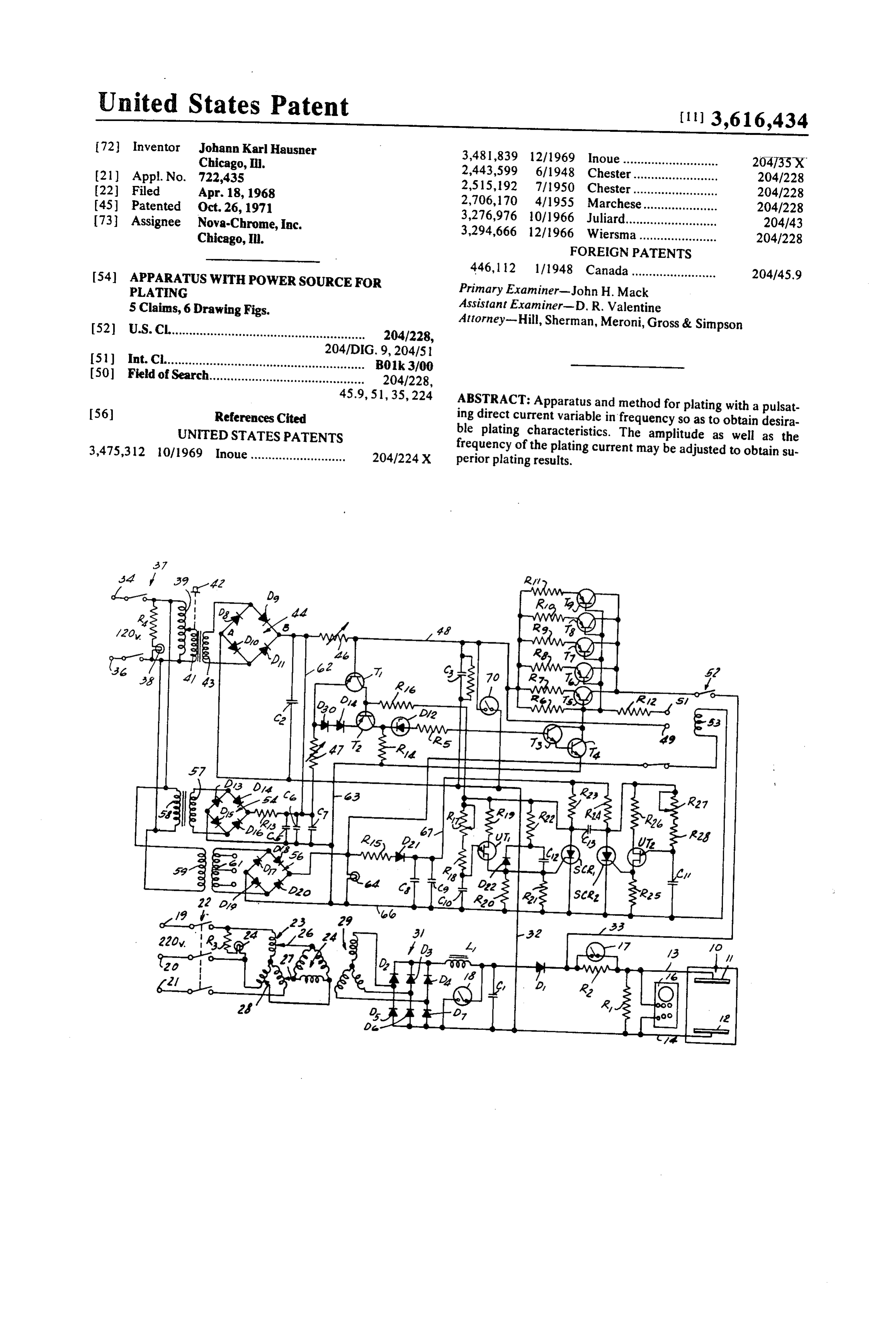
United States Patent (113,616,434 72 Inventor Johann Karl Hausner
Chicago, Ill. 3,481,839 12/1969 Inoue ........................... 204135X. 21 ) Appl. No. 722,435 2,443,599 6/1948 Chester... 204/228 22 Filed Apr. 18, 1968 2,515, 192 7/1950 Chester...... 204/228 45 Patented Oct. 26, 1971 2,706,170 4/1955 Marchese..................... 204/228 73) Assignee Nova-Chrome, Inc. 3,276,976 10/1966 Juliard.......................... 204/43 Chicago, Ill. 3,294,666 12/1966 Wiersma...................... 204/228
FOREIGN PATENTS
54) APPARATUS WITHPOWER SOURCE FOR 446,112 l/1948 Canada........................ 204/45.9 PLATING Primary Examiner-John H. Mack 5 Claims, 6 Drawing Figs. Assistant Examiner-D. R. Valentine 52) Attorney-Hill, Sherman, Meroni, Gross & Simpson U.S.C....................................................... 204/228,
(51) int. Cl.........................................................
50 Field of Search............................................ B01k 3/00
45.9, 51,35,224 ABSTRACT: Apparatus and method for plating with a pulsat 56) References Cited ing direct current variable infrequency so as to obtain desira UNITED STATES PATENTS ble plating characteristics. The amplitude as well as the 3,475,312 10/1969 Inoue ........................... frequency of the plating current may be adjusted to obtain su 204/224X perior plating results.
Page 2
Drawing sheet — no readable text.
Page 3
Drawing sheet — no readable text.
Page 4
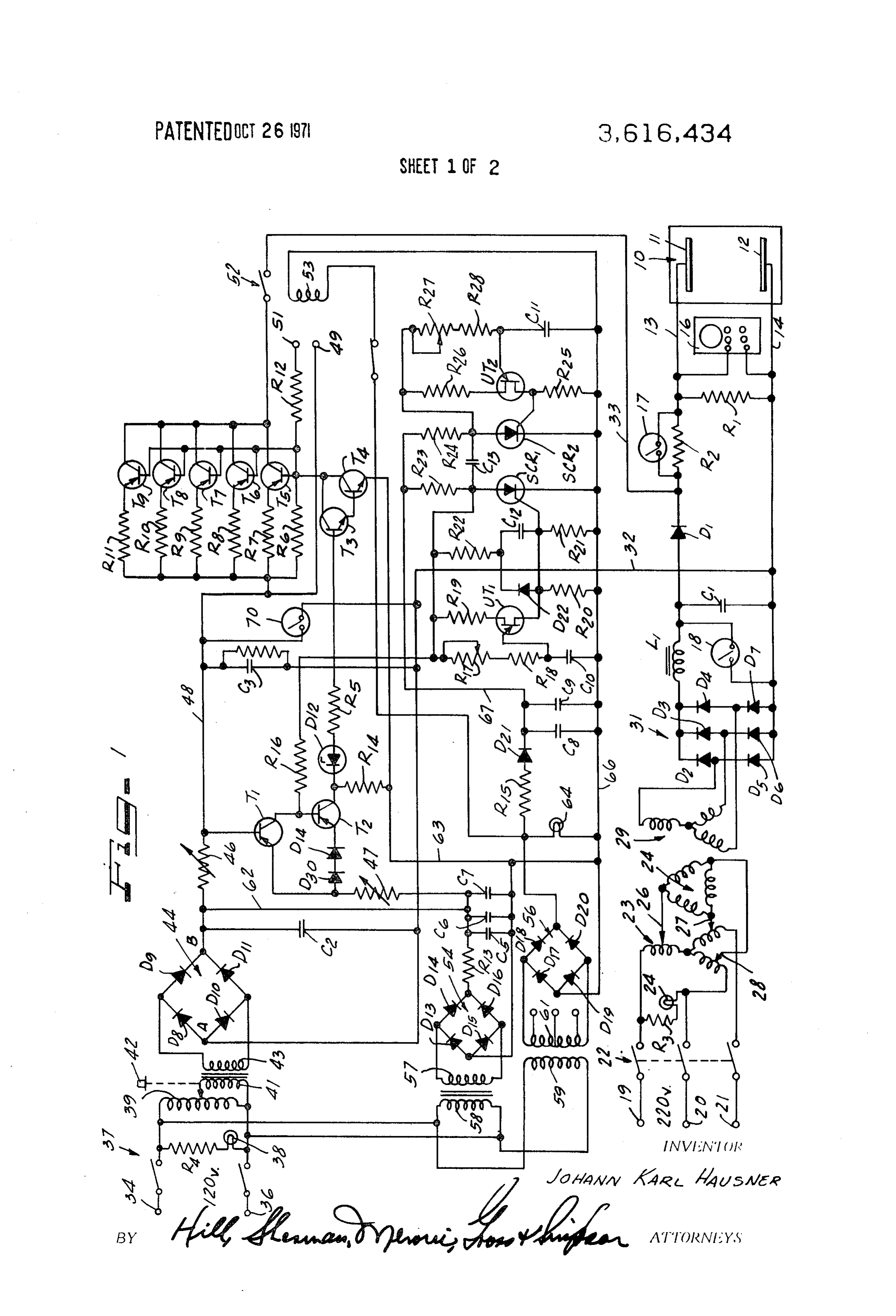
APPARATUSWTPOWER SOURCE FOR PLATING and through a circuit breaker 22 to a Y primary 23 of a trans BACKGROUND OF THE INVENTION former. A light 24, for indicating that power is on, is con 1. Field of the Invention nected between contacts 20 and 19 in series with a resistor Rs.
A delta-connected portion of the transformer is designated as
The invention relates in general to plating, and in particular 24 and is connected to adjustable wiper contacts 26, 27 and to a new and novel plating apparatus and method wherein an 28 which engage the Y-connected primary 23 to vary the volt alternating current is superimposed on a direct current ap age to the unit 24 of the transformer. A Y-connected output plied to a plating bath and the amplitude and frequency of su 29 is magnetically coupled to the portion 24 and is connected perimposed alternating current produces improved plating O to a full-wave rectifier designated generally as 31, and which characteristics. comprises the diodes D, through D. An inductor L is con 2. Description of the Prior Art nected between the diodes D, D and D and the diode D. My prior patent entitled "Electroplating," U.S. Pat. No. Thus the rectifier 31 supplies rectified direct current to the 2,824,830 discloses superimposing on a DC field in a plating plating bath. The inductor Li and capacitor C provide a bath at least two high-frequency fields of relatively high 15 smoothing filter. Lead 32 is connected to lead 14 and provides frequencies. an input lead for superimposing an AC pulsing signal on the SUMMARY OF THE INVENTION direct current supplied to the plating bath. A second lead 33 provides the second lead for providing the AC pulsating input
An improved apparatus and method of plating which uses to the plating bath. A pair of input leads 34 and 36 are con semiconductor devices for producing a direct current plating 20 nected to a suitable AC source as, for example, 120-volt sin signal upon which is superimposed alternating current pulses gle-phase alternating current power. The circuit breaker 37 is of varying amplitudes and which may be varied in frequency connected in circuit with input terminals 34 and 36. A resistor and in time on and time off to control the shape of the AC pull R and indicator light 38 are connected across the input ter ses and obtain much improved plating results over the prior minals 34 and 36. Primary 39 of an auto transformer is con art. An amplifier is provided which when connected in the cir 25 nected to terminals 34 and 36, and has a secondary 41 which cuit prevents feedback. has a slide contact that may be controlled by the knob 42. A Other and further objects of this invention will be apparent secondary 43 is coupled to the winding 41, and supplies an to those skilled in this art from the following detailed descrip input to a rectifier designated generally as 44, comprising the tion of the annexed sheets of drawings which, by way of a diodes D through D. Condenser C is connected across the preferred embodiment of the invention, illustrate one example 30 output terminals of the rectifier 44. A variable potentiometer of the invention. 46 is connected to point B and controls the time off of the al
BRIEF DESCRIPTION OF THE DRAWINGS
ternating current output. The potentiometer 46 is connected to the base of a transistor T which has its collector connected
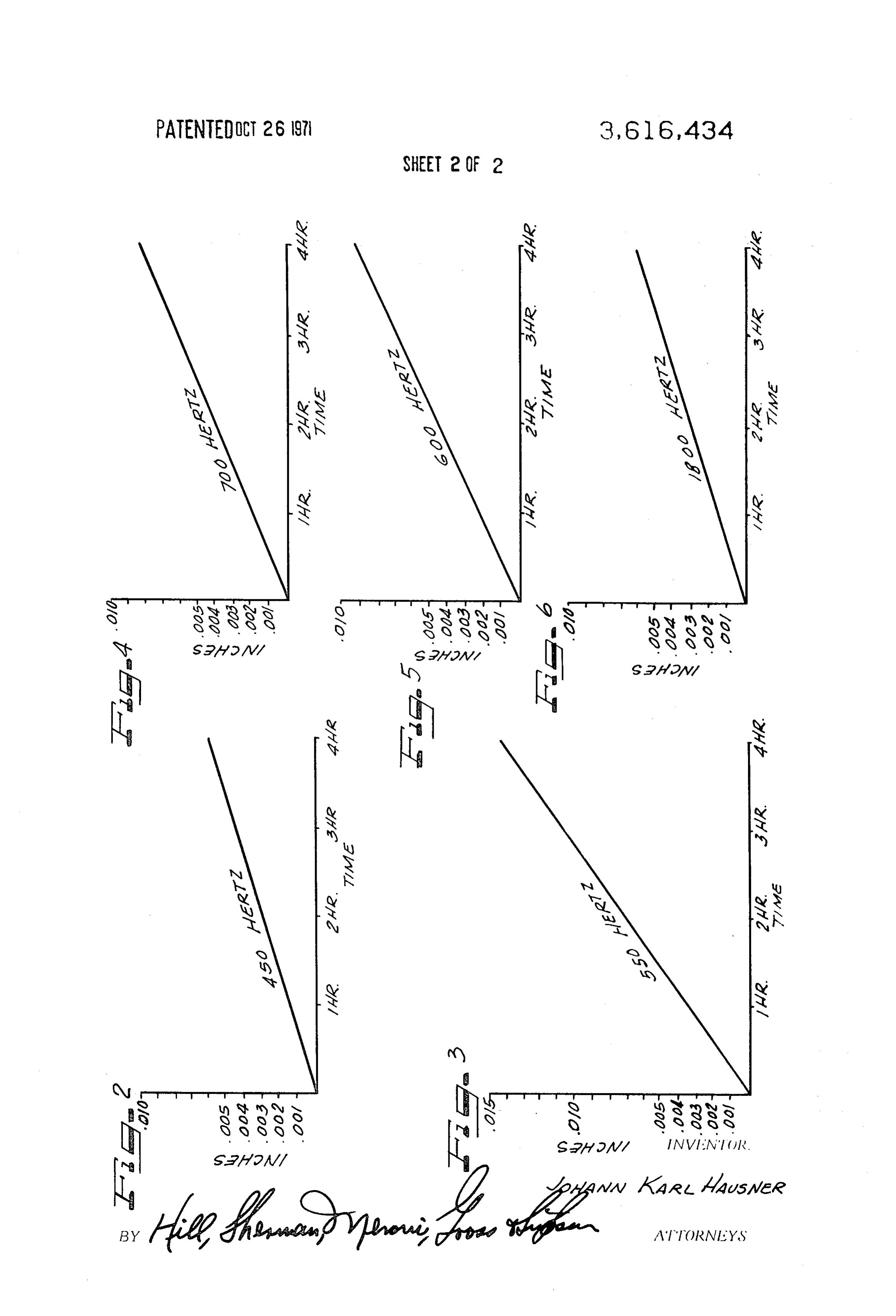
FIG. 1 is a schematic diagram of the plating apparatus of 35 to the base of a transistor T. The collector of transistor T is this invention. connected to a tunnel diode Ds. A time-on potentiometer 47 FIG. 2 is a graph of the plating response in which the AC is connected to the emitter of transistor I. A pair of diodes Dso signal has a frequency of 450 hertz. and D are connected in series between the emitters of FIG. 3 is a graph of the plating response using an AC pulse transistors T and T. A resistor Rs is connected between the of 550 hertz. 40 tunnel diode Ds and the base of a transistor Ta. The emitter of FIG. 4 illustrates a plating characteristic utilizing an AC the transistor Ta is connected to the base of transistor T. The pulse of 700 hertz; collector of transistor T is connected to the bases of FIG. 5 illustrates a plating characteristic utilizing a 600 transistors T through T. A lead 48 is also connected to the hertz signal; and potentiometer 46 and to resistors Rs through Ri which have FIG. 6 illustrates a plating response utilizing an AC signal of 45 their opposite sides connected to the emitters of the 1,800 hertz. transistors Ts through T. An input terminal for reverse bias 49 is connected to lead 48 and a terminal 51 is connected to the
DESCRIPTION OF THE PREFERRED EMBODIMENTS bases of the transistors Ts through T through the resistor R. Lead 33 is connected to the collectors of the transistors Ts
FIG. 1 illustrates a plating bath 10 which includes a cathode 50 through 11 and an anode 12 to which plating leads 13 and 14 are at T through a switch 52. The switch 52 is closed when tached, respectively. A cathode-ray oscilloscope 16 con the solenoid 53 is energized. A bias voltage is supplied by rectifiers 54 and 56 which respectively comprise diodes Dis nected across the leads 13 and 14 indicates to an operator the through Ds and diodes D, through Do. The rectifier 54 is wave shape of the applied signal to the plating bath.
For example, plating may be carried out in a chrome plating 55 connected its primary across the secondary 57 of a transformer which has 58 connected to the power leads 34 and 36. A pri aqueous electrolyte bath, having 250 grams per liter of CrO mary 59 of a transformer is also connected to the input power (as chromic acid), 1.8 percent sulfuric acid (HSO), 3 per leads 34 and 36 and has its secondary 61 connected to the cent boric acid (HBO), and 1 percent oxalic acid. In this rectifier bath, the essential pH control is provided by the sulfuric acid, rectifier 56. A resistor Rs is connected to one output of the 54 and condensers C, C and C are connected in but superior results are obtained by the use also of substan 60 parallel tially 0.5-5.0 percent boric acid and 0.1-3.0 percent oxalic resistor betweenR. A the other output lead of the rectifier 54 and lead 62 is connected between the resistor Rs acid. (Unless otherwise specified, the terms "parts' and "per and point B of the rectifier 44. The time-on potentiometer is centage' mean the same by weight). The plating bath is main also connected to the condensers Cs C and C. A lead 63 is tained at 135 F., while plating with a cathode current density connected to the output of the rectifiers 54 and 56 and a re of about 2-3 amperes per square inch. The anode may be lead 65 sistor R is connected between the lead 63 or other conventional material. The specific cathode A.S.I. of the transistor T. Lead 63 is also connectedand the collector to the emitter of
(DC) is measured when the pulsating current in operation is the transistor T. A light 64 is connected across the output of recited with other operating conditions in FIGS. 2 through 6, the rectifier 56. A resistor Rs is connected in series with a and under the conditions established in such figures. diode D, in one output line of the rectifier 56 and a pair of A resistor R is also connected across leads 13 and 14. An 70 condensers C and C are connected in parallel between the ammeter 17 is connected in line 13 and is bridged by a suitable leads 66 and 67. A resistor Rus and a variable resistor R and a shunt R. A diode D is connected to resistor R and a con resistor Rus and a capacitor Co are connected between the denser C is connected from line 14 to diode D. A voltmeter collector of transistor T and lead 66. A resistor R is con 18 is connected across condenser C. A source of 3-phase 220 nected from resistor Re to a unijunction transistor UT and volts, for example, AC is connected to terminals 19, 20 and 21 75 particularly to the base 1 terminal. The emitter terminal of the
Page 5
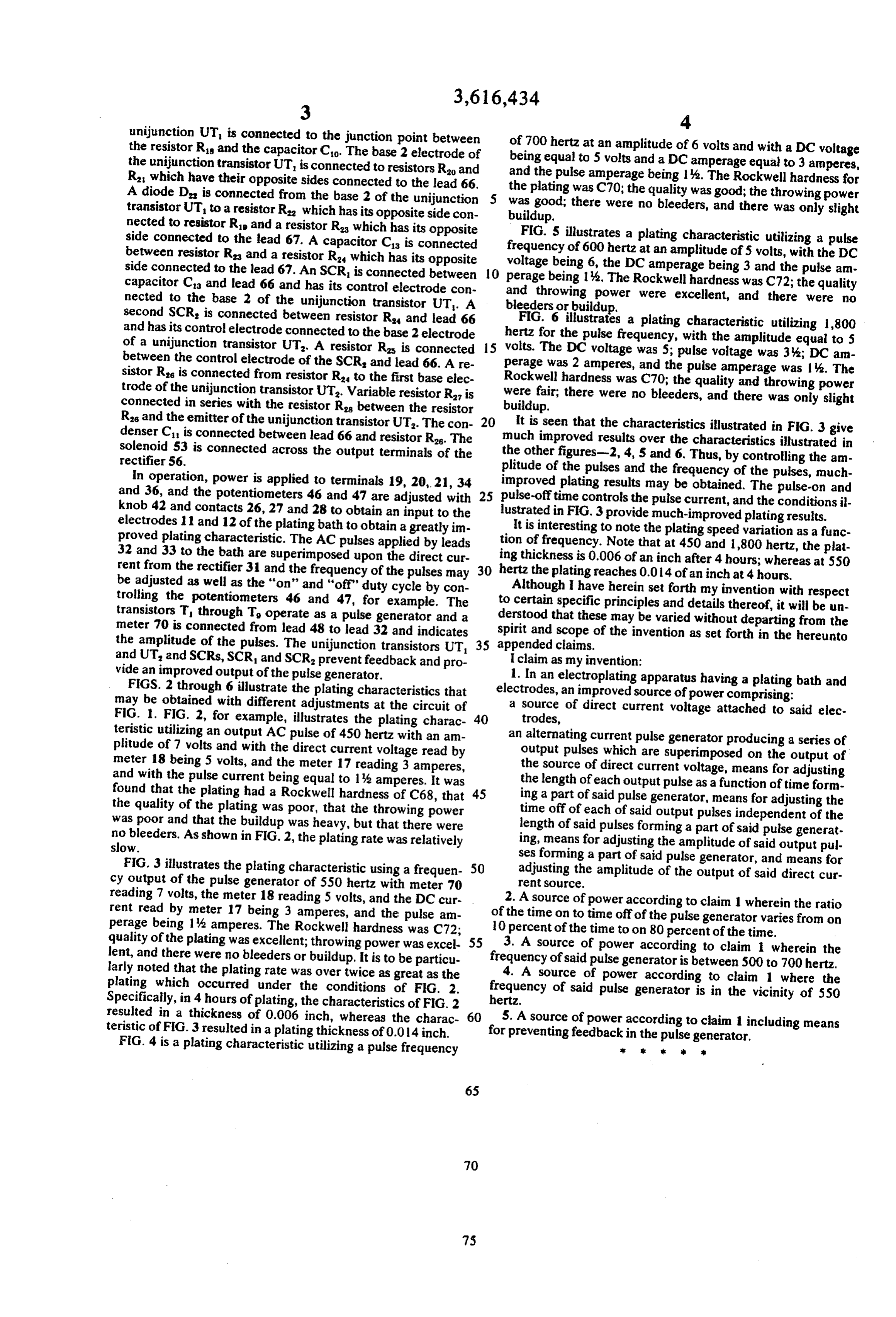
unijunction UT is connected to the junction point between the resistor Rs and the capacitor Co. The base 2 electrode of of 700 hertz at an amplitude of 6 volts and with a DC voltage being equal to 5 volts and a DC amperage equal to 3 amperes, the unijunction transistor UT, is connected to resistors Rao and and the pulse amperage being 1%. The Rockwell hardness for R, which have their opposite sides connected to the lead 66. the plating was C70; the quality was good; the throwing power A diode D, is connected from the base 2 of the unijunction was good; there were no bleeders, and there was only slight transistor UT to a resistor R, which has its opposite side con buildup.
nected to resistor R and a resistor Rs which has its opposite FIG. 5 illustrates a plating characteristic utilizing a pulse side connected to the lead 67. A capacitor Cs is connected frequency of 600 hertz at an amplitude of 5 volts, with the DC between resistor R and a resistor R, which has its opposite voltage being 6, the DC amperage being 3 and the pulse am side connected to the lead 67. An SCR is connected between 10 perage being 1%. The Rockwell hardness was C72; the quality capacitor Cia and lead 66 and has its control electrode con and throwing power nected to the base 2 of the unijunction transistor UT. A bleeders or buildup. weree excellent, and there were no second SCR is connected between resistor R and lead 66 FIG. 6 illustrates a plating characteristic utilizing 1,800 and has its control electrode connected to the base 2 electrode hertz for the pulse frequency, with the amplitude equal to 5 of a unijunction transistor UT. A resistor Rs is connected 15 volts. The DC voltage was 5; pulse voltage was 3%; DC am between the control electrode of the SCR and lead 66. A re perage was 2 amperes, and the pulse amperage was 1%. The sistor Rs is connected from resistor R to the first base elec Rockwell hardness was C70; the quality and throwing power trode of the unijunction transistor UT. Variable resistor R is were fair; there were no bleeders, and there was only slight connected in series with the resistor Rs between the resistor buildup.
Rs and the emitter of the unijunction transistor UT. The con 20 It is seen that the characteristics illustrated in FIG. 3 give denser C is connected between lead 66 and resistor Rs. The much improved results over the characteristics illustrated in solenoid 53 is connected across the output terminals of the the other figures-2, 4, 5 and 6. Thus, by controlling the am rectifier 56.
plitude of the pulses and the frequency of the pulses, much
In operation, power is applied to terminals 19, 20, 21, 34 improved plating results may be obtained. The pulse-on and and 36, and the potentiometers 46 and 47 are adjusted with 25 pulse-off time controls the pulse current, and the conditions il knob 42 and contacts 26, 27 and 28 to obtain an input to the lustrated in FIG. 3 provide much-improved plating results. electrodes 11 and 12 of the plating bath to obtain a greatly im proved plating characteristic. The AC pulses applied by leads tionIt isofinteresting to note the plating speed variation as a func frequency. Note that at 450 and 1,800 hertz, the plat 32 and 33 to the bath are superimposed upon the direct cur ing thickness is 0.006 of an inch after 4 hours; whereas at 550 rent from the rectifier 31 and the frequency of the pulses may 30 hertz the plating reaches 0.014 of an inch at 4 hours. be adjusted as well as the "on" and "off' duty cycle by con trolling the potentiometers 46 and 47, for example. The to Although I have herein set forth my invention with respect transistors T, through T operate as a pulse generator and a derstood that theseprinciples certain specific may be and details thereof, it will be un varied without departing from the meter 70 is connected from lead 48 to lead 32 and indicates spirit and scope of the invention as set forth in the hereunto the amplitude of the pulses. The unijunction transistors UT 35 appended claims.
and UT, and SCRs, SCR and SCR preventfeedback and pro I claim as my invention:
vide an improved output of the pulse generator. 1. In an electroplating apparatus having a plating bath and FIGS. 2 through 6 illustrate the plating characteristics that electrodes, an improved source of power comprising: may be obtained with different adjustments at the circuit of
FIG. 1. FIG. 2, for example, illustrates the plating charac 40 a trodes, source of direct current voltage attached to said elec teristic utilizing an output AC pulse of 450 hertz with an am an alternating current pulse generator producing a series of plitude of 7 volts and with the direct current voltage read by output pulses which are superimposed on the output of meter 18 being 5 volts, and the meter 17 reading 3 amperes, the source of direct current voltage, means for adjusting and with the pulse current being equal to 1% amperes. It was the length of each output pulse as a function of time form found that the plating had a Rockwell hardness of C68, that 45 ing a part of said pulse generator, means for adjusting the the quality of the plating was poor, that the throwing power time off of each of said output pulses independent of the was poor and that the buildup was heavy, but that there were length of said pulses forming a part of said pulse generat
slow.
bleeders. As shown in FIG. 2, the plating rate was relatively ing, means for adjusting the amplitude of said output pull ses forming a part of said pulse generator, and means for
FIG. 3 illustrates the plating characteristic using a frequen 50 adjusting the amplitude of the output of said direct cur cy output of the pulse generator of 550 hertz with meter 70 rent source.
reading 7 volts, the meter 18 reading 5 volts, and the DC cur rent read by meter 17 being 3 amperes, and the pulse am of2.theAtime source of power according to claim 1 wherein the ratio on to time off of the pulse generator varies from on perage being 1% amperes. The Rockwell hardness was C72; 10 percent of the time to on 80 percent of the time. quality of the plating was excellent; throwing power was excel 55 3. A source of power according to claim 1 wherein the lent, and there were no bleeders or buildup. It is to be particu frequency of said pulse generator is between 500 to 700 hertz. larly noted that the plating rate was over twice as great as the 4. A source of power according to claim 1 where the plating which occurred under the conditions of FIG. 2. frequency of said pulse generator is in the vicinity of 550 Specifically, in 4 hours of plating, the characteristics of FIG. 2 hertz.
resulted in a thickness of 0.006 inch, whereas the charac 60 5. A source of power according to claim 1 including means teristic of FIG.3 resulted in a plating thickness of 0.014 inch. for preventing feedback in the pulse generator. FIG. 4 is a plating characteristic utilizing a pulse frequency r t
Provenance
- Collection
- Cited prior art
- Original PDF
- patentimages.storage.googleapis.com →
- Filed
- 1968-04-18
- Pages
- 5
- Method
- pdftotext (the PDF's own text layer) + pdftoppm 300dpi page scans
- Source
- Google Patents bibliographic record
- Granted
- 1971-10-26
- Inventors
- Johann Karl Hausner; NOVACHROME Inc
- Transcribed from
- patentimages.storage.googleapis.com →