patent · US3232745
Producing rod-shaped semiconductor crystals
1 February 1966
Page 1
Drawing sheet — no readable text.
Page 2
United States Patent Office Patented Feb.3,232,745
conductor substance at a molten zone at the upper end
PRODUCING ROD-SHAPEED SEMECONDUCTOR of a rod-shaped carrier crystal, to which the semicon CRYSTALS ductor substance is supplied in finely divided and espe Theodor Rummel, Munich, Heinrich Kniepkamp, Karls cially in atomic condition, thus continuously giving of rule, and Reiner. Emeis, Fretzfeld, Upper Franconia, material for progressive cooling or solidification on the Germany; assignors to Siemens & Halske Aktiengesell-- solid crystal carrier. The advantage of arranging the schaft, Berlin. and Munich, Germany, a German corporation . molten area at the upper end of the seed crystal resides in the fact that the melt rests upon a solid support which
Filed Dec. 5, 1960, Ser. No. 73,809 secures it in relatively high degree against dropping off. 7 Claims. (C. 75-10) 0. However, the interface between the melt and the solid This invention is concerned with producing rod-shaped crystal body extends as a rule not along a plane area but semiconductor crystals from a gaseous phase containing is upwardly arched, since the cooling is primarily effected the corresponding semiconductor substance, the present by heat conduction over the solid crystal body while the disclosure being a continuation-in-part of copending ap heating is effected by radiation from the outside. When plication Serial No. 510,493, filed May 23, 1955, now it is intended to work instead of with a thin molten skin, patent No. 2,964,396, dated December 13, 1960, owned with a relatively substantial amount of molten material, by the assignee also named in the present case. which is desirable in the interest of improved crystal In accordance with a previously known method, the lization, there will appear the drawback that the melt is desired semiconductor material is produced by decomposi poorly localized in its position with respect to the crystal tion, in an electric gas discharge, of a gaseous compound 20 rod, such melt constantly assuming a changed position which contains the corresponding semiconductor sub at the tip of the seed crystal. The reason for this situa stance and which is intermixed preferably with purified tion is that the melt is in the known methods relatively hydrogen gas as a reducing agent, the material being de well secured against dropping off, but the position thereof posited or precipitated on the electrodes provided for the with respect to the solid crystal carrier corresponds to a gas discharge and caused to crystallize thereon. maximum of potential energy or at best to a condition of It has also been proposed to employ the above indicated indifferent equilibrium. The disadvantage resides in the prior method for producing semiconductor rods. An fact that the position of the melt is changed even respon- . electric arc discharge is for this purpose effected in a sive to slight disturbances, for example, such as are caused reaction gas containing the desired semiconductor sub by gas flow or by the motion imparted to the crystal stance, such discharge causing separation of the elemen 30 carrier, resulting necessarily in irregular diameter of the tary semiconductor substance from the reaction gas. Un drawn body. The rodlike bodies are accordingly if irreg derneath the area of the arc discharge is disposed a carrier ular diameter and poor crystal quality, resulting in the or seed crystal made of the corresponding semiconductor further processing thereof to produce semiconductor de Substance in the shape of a short crystal, which catches vices, in great waste of costly semiconductor material. the finely distributed semiconductor material produced by The present invention recognizes that the above in the gas discharge. The upper end of the carrier crystal dicated disadvantages can be avoided in relatively simple is thereby melted, the hot molten part preferentially re manner by arranging the melt, on which the semiconduc ceiving the separated semiconductor material. The car tor Substance is to be precipitated from the gas phase, rier crystal is gradually drawn downwardly, away from the 40 not at the upper end but at the lower end of the carrier : area of the arc discharge. The lower part of the molten which is made of the same material. area on which the separated material is precipitated is The present invention is accordingly concerned with a . thus cooled, cauging continuous crystallization thereof method of producing rod-shaped semiconductor crystals, and thereby effecting gradual growth of the rod-shaped comprising causing a reaction gas which contains the re seinicoductor body. The speed of downward withdrawal spective semiconductor substance or components thereof of the growing rod-shaped semiconductor body is adjusted to interact with a melt carried by a solid crystal body to the rate of Separation of the material from the gaseous made of the corresponding semiconductor substance, said phase, so that the size of the molten area and its position melt receiving the substances liberated from the reaction with respect to the gas discharge zone remain as constant gas by decomposition and forming the desired semicon as possible. ductor material, and thereby effecting continuous growth Instead of utilizing a gas discharge, purely thermal de of the solid crystal by crystallizing the substance precip composition or reaction may be employed for separat itated thereon. In accordance with the invention, the ing the semiconductor material on a seed crystal made of melt which is to be utilized is produced by melting the the Same material. Localization of the separation is in crystal body at the lower end thereof, such melt depend such case likewise possible, provided that only part of ing from the crystal body in the fashion of a drop on the Surface of the carrier seed is caused to melt, since 55 which liberated material is precipitated by the action of the formation of the liberated semiconductor material an energy source, the crystal body being withdrawn up starts and is primarily effected at the hottest portions of Wardly at a speed adjusted to the rate at which mate the carrier. In accordance with a prior method, a rod rial is precipitated, thereby withdrawing the solid crystal shaped semiconductor crystal is melted at its upper end, body from the range of action of the energy source while and the corresponding melt is contacted with a reaction 60 maintaining the size of the melt substantially constant, gas containing the semiconductor substance. The hot The advantages which will be presently described more surface of the melt, acting as a catalyzer, favors the de in detail and which have to do with utilizing a melt in composition or reduction of the reaction gas, whereby the the form of a downwardly depending drop, will be se semiconductor substance is separated predominantly on cured by the provision of means for additionally support the surface of the melt and precipitated thereon. A 65 ing such melt drop. The support can be effected, for ex semiconductor rod of desired length can be produced by gradually withdrawing it from the range of the heat ample, pneumatically or by the action of an electromag netic field, and in the latter case, if there is provided an source which produces the melt, the melt thereby sub electromagnetic energy source, by the action of such stantially retaining its relative position with respect to the Source. The molten drop may also be supported, with heat source.
The prior methods provide for the separation of semi of out foregoing the advantages flowing therefrom, by means a crystal body disposed therebelow, the molten drop
Page 3
resting thereby in the form of a molten zone extending od proposed by the present invention is considerably better between the two vertically coextensive solid crystal bodies. itforisproducing mono crystals than the prior method, when considered that the use of a melt depending down . A downwardly depending molten drop would at first appear to be a relatively unstable structure which would awardly from the crystal body in the form of a drop forms crystallization. plane which is on top while the crystal be easily excited to execute resonance oscillations favor ing dropping off, and would be in this respect inferior lization plane in the case of a melt provided at the upper to a melt disposed at the upper end of the carrier; how end of a crystal body is situated at the botton. ever, the downwardly depending molten drop has the The foregoing and further objects and features of the considerable advantage that it always assumes the lower invention will appear in the course of the description most position on the seed crystal. This is due to the fact which is rendered below with reference to the accom that the melt corresponds in this position to a condition panying drawing showing embodiments thereof. of least potential energy. Accordingly, the position of The danger that the meit drops off is naturally greater the melt on the carrier will remain invariable in the inter in the method according to the present invention than in play between melting action and crystallization action, the prior methods. The use of a large amount of molten since the melt, after decay of a disturbance, wili automat material is on the other hand required in the interest of ically assume its lowermost position at the seed crystal. good crystallization. It is in view of these aspects de When the size of the molten drop is held constant, by ad sirable that means be provided for increasing the mechani justment of the speed of crystallization to the speed of cal stability of the melt without producing a contamina semiconductor precipitation or separation from the reac tion thereof. A simple way of satisfying this requirement tion gas, which is easily effected, the size of the interface 2 resides in supporting the melt pneumatically by employ surface with the solid seed crystal will likewise remain ing for this function the stream of reaction gas flowing constant in the course of operation. into the apparatus. This can be effected as shown in The use of a downwardly depending drop-shaped melt FIG. 1, by blowing the reaction gas discharged from a at the lower end of the seed crystal must therefore neces 25 nozzle against the downwardly depending molten drop so sarily result in uniform rods growing in straight manner. as to support it. The same function can of course be Even upon using at the start of the operation an irregular fulfilled by an inert protective gas. Another possibility of increasing the stability of the ly, shaped seed crystal as a carrier, the cross-section of the rod produced will quickly stabilize to a constant value, melt resides in supporting the corresponding moiten drop since the downwardly depending molten drop which is by means of the action of an electromagnetic field. As held at a constant volume leads necessarily to uniformity 30 is known, an electromagnetic field can induce eddy cur of a crystallization front which might have been irregular. rents in a conductive or in a semiconductive material, at the start of the process, such eddy currents imparting to the material a magnetic The precipitation or separation of the semiconductor moment. However, to a body having a magnetic moment substance at the hottest point in the reaction vessel, which 35 is imparted a force, in a non-homogeneous or an electro is represented by the downwardly depending molten drop, magnetic field, which endeavors to pull the body either is at any rate secured, since the surface of the hot melt into a region of higher field strength or to crowd it from as catalyzer in the liberation of the semiconductor sub the region of higher fieldstrength. The induced magnetic stance from the reaction gas. The uniformity of the moment is, in the case of a non-homogeneous field, in ac growth of a rod is assured to a high degree by the inven 40 cordance with the known rule supplied by Lenz, so orient tion, since. no noticeable distortion can be caused by the ed that it attempts to crowd the body out of the region of crystallization on the solidified but still hot rod incident to higher field strength. When the electromagnetic field the withdrawal thereof. affecting the body increases in the direction of the force However, if the melt is produced at the upper end of of gravity, the field will tend to move the body in opposite the seed crystal, as in the previously known methods, its direction. The force of the field with respect to the solid position, while affording greater security against drop or fluid body depends upon the amount of the magnetic ping off, will correspond to a maximum of the potential moment induced in the body and upon the magnitude of energy and therewith to an unstable equilibrium condi the gradient of the electromagnetic field. It can according tion. While a case in which the adhesion is opposed to ly be made very great by an appropriately high field gradi the force of gravity can never occur, whereby the acute 50 ent in the direction of the force of gravity as well as by a danger of dropping off is largely avoided, the position of sufficiently high amplitude and/or frequency of the alter the melt on the seed crystal is nevertheless by no means nating field. The levitation, imparted to a conductive invariable, as already explained before, but depends to body in such field, stops as soon as the body assumes a a high degree upon chance. The size and position of the, position in the field in which the force thereof balances recrystallization front is accordingly subjected to consider the weight of the body. i - ably greater fluctuations than in the case of a downward 55 Such a field is supplied by a short coil which is tra ly depending drop, and the production of uniformly grown versed by alternating current, the axis of the coil coin rods is consequently extraordinarily difficult in connection ciding with the axis of the crystal carrier rod, with the with the previously known methods. molten drop situated somewhat above the symmetry plane As an additional disadvantage of the prior method may O of the coil, in some situation even somewhat above the be mentioned the fact that it is very difficult to produce upper margin of the coil, the coil field being in such a with the use thereof mono crystal rods. It must be con case oriented radially symmetrical to the axis of the carrier sidered in this connection that the size of the melt and and the molten drop adhering to the lower end thereof, therewith its temperature cannot be maintained as desired and moreover diverging upwardly at any point of the above the melting point of the corresponding semicon 65 molten drop. It follows, therefore, that an upwardly di ductor and, accordingly, it may easily happen that islands rected and at the same time inwardly oriented supporting of solidified semiconductor material are formed on the force will be operative with respect to all parts of the melt surface of the melt due to cooling. This possibility is adhering in drop shape to the carrier. The dimension above all present in the neighborhood of the crystalliza ing of the field strength as well as of the field gradient are tion plane. These islands have as is known the tendency 70 a matter of experience and therefore must be determined to sink downwardly and they can thus directly reach the experimentally, depending especially upon the size of the crystallization plane and be built thereinto if such plane motten drop. The endeavor should be to place the meridi is at the deepest point of the melt. The building-in of an lines of the drop so that they form with peripheral these islands into the crystallization plane usually results lines of the crystallized rod an approximately obtuse angle in a polycrystalline degeneration of a previously present 5 at the border between the solid and the fluid phase. The monocrystalline growth. It will be realized that the meth condition is still more favorable, in individual cases, for
Page 4
example, in the processing of silicon, when the drop ex ing of the crystal body upon start of the induction tends somewhat (about 10 percent) beyond the periph operation.
eral lines which delimit the crystallized material. The choice of reaction gas to be employed will depend A third possibility for supporting the downwardly de upon pending drop-like melt resides in the provision of a further 5. duced.theInkind the of semiconductor rod which is to be pro case of silicon rods to be produced, the crystal body similar to the carrier crystal and disposed materials to be considered aside from SiCl, include higher thereunder for supporting the melt from below, such silicon halides such as siliconhexachloride or siliconocto melt accordingly appearing as a molten zone between chloride as well as halogenated silanes such as silicon the two vertically coaxially arranged solid crystal bodies. chloroform or corresponding higher homologs. In the These crystal bodies are drawn apart at a speed corre-10 case of germanium rods to be produced, there will be em sponding to the rate of growth of material at the melt, ployed corresponding or appropriate germanium com thus withdrawing them from the range of action of the pounds. In order to facilitate separation of the semi energy source which produces the melt. The operation conductor substance, hydrogen may be intermixed with can be effected by using the arrangement shown in FIO. 2. the
The advantages obtained from a downwardly depend- 15 Inreaction the gas, the hydrogen acting as a reducing agent.
method according to the invention, the separation ing molten drop are, upon use of the second crystal body of the silicon or other semiconductor material is effected for supporting it, preserved at least with respect to the predominantly on the surface of the melt. In addition portion of the rod extending upwardly from the melt. thereto, and especially when using silane, there may occur Moreover, as compared with a melt produced at the upper spurious silicon production in the free gas space, which end of a seed crystal, the position of the contacting plane 20 may be effected in some situation by the temperature field with the lower crystal body is considerably stabilized. of the melt, although such spurious separation would be This particular embodiment of the invention permits espe very much less as compared with the separation at the cially quick execution of the operation, involving draw ing apart of the two crystal bodies according to the rate melt. In order to assure that silicon which is thus spuri at which material is separated at the melt, since crystalli- 25 ously produced will reach the melt, gas streams, especially streams of the reaction gas may be directed against the zation is effected at the upper as well as at the lower crys melt or electrical means may be employed for this pur tal bodies. The molten zone can be advantageously pro pose. It is proposed to use for this purpose above all the duced by melting a portion of a vertically extending rod So-called electric blast, an electric stream in the reaction like semiconductor crystal body along a zone of limited length. space, which is produced, for example, by means of points. 30 or knife edges disposed opposite the melt which is
Various known means can be additionally employed in grounded, such points or knife edges being charged with realizing the present invention. Thus, axial rotation of high voltage. The electric blast is a phenomenon which the rod or of the parts of the rod which carry the molten, is well known in the electrostatic field. Such phenome zone, will benefit the uniformity of the heating of the melt, non is based upon the fact that a relatively very high thereby improving the properties of the crystal to be pro- 35 field strength will obtain in the vicinity of edges or points duced. In the case of round rods, the melt can be main of electrically charged bodies even in the presence of tained in rotation by the use of an electric rotary field. relatively low voltages. However, since the gas surround The material of the melt is for this purpose permeated by ing such body loses in the presence of high field strength. a magnetic field which is produced, for example, by two magnet poles which are oppositely disposed alongside the 40 its insulation property, due to ionization, thus becoming conductive, a discharge will occur at such edges or points.
melt but out of engagement therewith. The magnet field This discharge imparts to the atoms or molecules of the will become a rotary field responsive to rotation of the gas a mechanical motion directed away from the points or magnet poles about the axis of the melt, such magnet field: (edges, such motion being referred to as electric blast. In inducing a current into the molten material. The rule: the present case, there are provided two or more elec supplied by Lenz, as a direct consequence of Faraday's 45 trodes made of a metal, for example, tungsten, which is induction law, requires, that the induction action, effected difficult to melt, such electrodes being provided with points in the molten material by the rotation of the magnetic extending in the direction of the melt and the crystal body field, is subjected to local alteration, whereby the mate carrying it, and a direct voltage of a few thousand volts rial of the melt is brought into a condition of rotation in is applied thereto, such voltage being however too low to the direction of rotation of the magnetic field. Another 50 effect a visible gas discharge. An electric blast will thus and easier possibility for producing the rotating field re be produced in the reaction gas, which is directed toward sides in utilizing a three-phase current. Such current is the melt, thereby blowing the semiconductor material conducted to a coil system, in a manner known from three Separated in the free gas space thereagainst. phase motors, the melt functioning as the "rotor." The In the arrangement for realizing the invention, as illus coils are so oriented with respect to the melt, that the 55 trated in FIG. 1, the seed crystal 3 is, for example, a rod magnetic lines of force permeate the melt in a direction shaped extending perpendicular to the axis thereof, that is, hori cally in highly pure silicon body which is disposed verti a quartz tube 1, to the lower end of which is fused
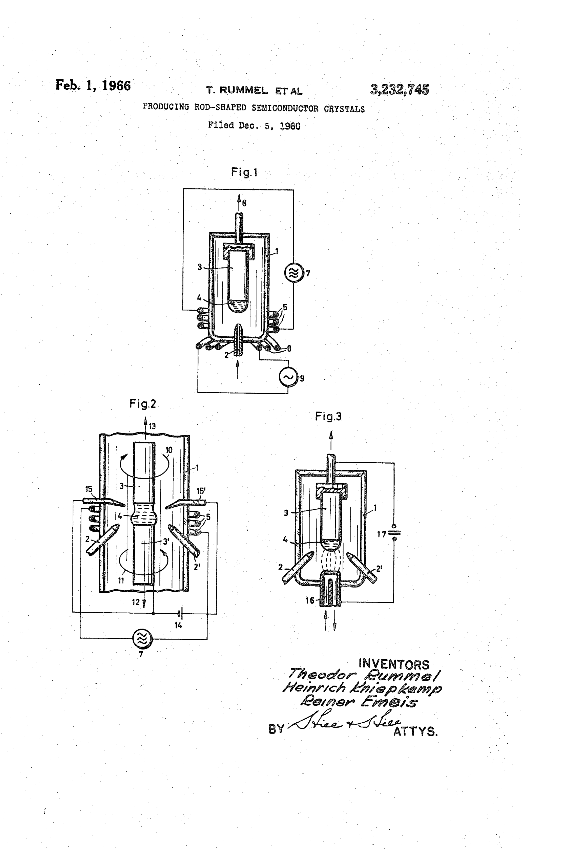
Zontally. a tubular nozzle 2, such nozzle serving as an inlet for the The melt may be produced in various manner, for reaction gas, for example, SiCl3 and H. An induction example, by radiation, atomic recombination energy or 60 coil 5 supplied with high frequency current from the by electron or ion bombardment, respectively. Heating Source 7, which surrounds the lower end of the seed crys with high frequency is particularly advantageous and eas tal rod 3, serves for producing the molten drop 4 at the ily applied, the lower end of the rod being thereby concen lower end thereof. The arrangement of the gas inlet 2 trically surrounded by an induction coil which is supplied underneath the molten drop 4, with the gas blowing there with alternating current, especially high frequency cur- 65 against provides a pneumatic support for the drop and rent, and being thus inductively heated. As already men Supply thereto of fresh reaction gas for direct contact tioned, this results in the advantage of simultaneously with the melt, the gas giving off to the melt the major part effecting an electromagnetic support for the melt by the of the silicon contained therein. The gas streaming up action of the field of the induction coil, as soon as the melt Wardly from the surface of the melt is relatively lean so is positioned above the median plane of the coil, such posi- 70 far as Semiconductor material is concerned, and the possi tion being automatically assumed by the upward with bility ofisseparation on the solidified but as yet hot rod drawal of the solid crystal body, away from the range of portion thus greatly reduced. heating. The seed crystal is in the case of highly pure semiconductor material usually extremely high ohmic, and 4 isThetaken silicon separated at the surface of the molten drop up thereby and would accordingly effect con it will therefore be of advantage to provide for a preheat- 75 tinuous increase of the size thereof. The seed crystal 3 is
Page 5
however continuously upwardly withdrawn in the direc strength of the coil current being increased until the lower tion of the arrow 6, with a speed such that the upper por end is melted to form the drop depending therefrom. tion of the fluid drop is cooled off and solidifies upon leav The use of preheating, for example, by means of an infra ing the induction field of the coil 5. The drawing speed red beam (not shown), directed against the lower end of and the reaction rate are mutually adjusted so that the crystal 3, which is to be melted, or the use, for this amounts of material of the drop 4 are crystallized on purpose, of a radiation produced by another device, for the solid rod 3 which correspond to the amounts separated example, illumination, will contribute toward consider from the reaction gas. The size of the molten drop and ably accelerating the melting operation even in the case therewith the size of the crystallization plane remain ac of high ohmic semiconductor material. m cordingly constant. In order to adjust the speed of crys 0. The energy of the high frequency coil is increased from tallization to the drawing speed, cooling means may be initially low values until the lower end of the crystal 3 provided for accelerating the speed at which the material is molten to form the drop depending from a crystal part solidifies. However, in the case of silicon, this will not be which remains in solid state. The size of the drop is necessary. The reaction vessel as well as the gas supply ascertained by experience and numerical values that conduits may be suitably cooled so as to prevent excessive 5 would be valid for all cases cannot be given. The drop heating thereof and therewith separation thereon of the shall however be of a size such that its profile forms with semiconductor material. . the profile of the solid crystal portion an angle as ex The symmetry plane of the induction coil is positioned tended as possible or, as will be better in many cases, for somewhat below the molten drop. The drop is accord example, in the case of silicon, that the profile of the drop ingly positioned within a range of the electromagnetic field 20 extends somewhat beyond the solid crystal. In the event possessing a gradient which effects a force operating in a that this is impossible owing to the surface tension of direction opposite to that of the force of gravity, thereby the molten material, the drop must be supported addi supporting the drop electromagnetically. The dimension tionally. The melting is suitably effected in hydrogen ing of the supporting force is a matter of experience and is gaS.
increased by increasing the coil current. It is, however, 25 The meling can be easily observed through a dark advisable to effect the support of the drop independent of colored glass, since the molten material distinguishes the heating source. This can be effected electromagneti optically from the solid material, and no difficulties will cally in the following manner: therefore be experienced in imparting to the drop a size An induction coil which is traversed by current pro Such as indicated above. The appearance of instability duces in known manner a magnetic field with the lines of 30 is clearly recognized by a constriction starting to form force diverging at the ends upon leaving the coil. The with respect to the profile of the drop, and such condition magnetic field accordingly posseses a noticeable field gra can be counteracted and cancelled out by appropriate dient which effects a translating force with respect to a . regulation of the heating of the drop. The danger of body having a magnetic moment. If the windings of the 35 the dropping off of the molten drop can thus be easily pre induction coil surround the extended axis of the crystal vented by careful work. The effect of supporting meas member 3 circularly, with the coil windings being dis ures, for example, by electromagnetic support of the drop posed along planes extending approximately perpendicu can likewise be clearly observed. larly to the vertical axis of the crystal member, the gra The reaction gas, for example, siliconchloroform inter dient of the field at the upper end will be in the direction 40 mixed with hydrogen is admitted into the reaction vessel of the force of gravity, and the gradient at the iower end as soon as the drop is of the desired size and the energy of the coil will be in a direction opposite to that of the Source which produces it adjusted so as to provide for sub force of gravity. The melt is due to the induction effect stantially constant drop size. The supply of the reaction traversed by eddy currents, therefore having a magnetic gas is in FIG. 1 effected through the nozzle 2 which is moment the direction of which is, in accordance with the disposed underneath the drop. 4, the purified reaction gas Lenz rule, so oriented that the met receives a force blowing against the drop in a uniform stream. There opposed to the field gradient, and it will be clear, there action gas decomposes at the hot surface of the drop, fore, that a force will act on the molten drop which is thereby separating pure silicon which is taken up by the opposed to the force of gravity when the drop is situated drop, the lean spent gases moving upwardly for discharge. within the range of the upwardly diverging magnetic lines The amount of separated material grows with the growth of force. This will be assuredly the case when the wind 50 of the drop surface and the drop temperature (which gen ings of the induction coil surround the crystal 3 concen erally must not be considerably increased above the melt trically and when the drop is situated somewhat above ing point of the material involved), and further with the the coil. The heating coil acts in such a case also as a anount of the silicon-containing compound in the re supporting coil. action gas which contacts the drop in a time unit. The However, it is also possible to provide below the heat 55 annount of the separation also depends upon the kind of ing coil an auxiliary coil 8, operaitng particularly as a the compound and can be calculated in accordance with supporting coil, which is traversed by a low frequency known rules governing thermodynamics. Accordingly, current from a source 9. The heating is not particularly the increase in the size of the drop, in a unit of time, increased by the action of the auxiliary field, owing to the effected by the separation of the material, can be easily . low frequency, but the supporting force is considerably 60 determined by calculation.
increased. However, it will generally suffice to rely upon visual , The embodiment according to FIG. 1 may be realized observation and to start withdrawing the solid crystal body by initially mounting in the reaction vessel 1 a cylindrical as soon as the drop begins to grow noticeably due to the body 3 of monocrystalline silicon, about 5 centimeters Separation thereon of the silicon, thus also obtaining in long and 20 millimeters thick, after first cleaning such 65 simple manner based upon observation, the withdrawal body with fluoric acid and drying it. The silicon crystal speed and the progressive cooling connected therewith. body 3 may also be subjected to thorough cleaning by means of etching. The reaction vessel , thus provided to The withdrawal speed is so adjusted that it is proportional with the silicon crystal 3, is thereupon relieved of any the speed of material separation or precipitation there residual moisture by conducting therethrough a stream of O of, which is recognized by observing that the drop size hydrogen. The induction coil 5 is thereafter placed in po remains constant during the progress of the separation. sition so that its windings are situated concentrically about Fluctuations in the size of the drop are in simple manner the extended axis of the lower end of the crystal 3 or equalized or compensated by constantly effected increase. better somewhat below the lower end thereof. High fre or decrease of the drawing speed or by increase or de quency energy is then supplied to the induction coil, the 5 crease of the supply of reaction gas, respectively.
Page 6
9 O
In the example shown in FIG. 2, the melt is in the form Changes may be made within the scope and spirit of of a fluid zone 4 which extends between two solid highly the appended claims which define what is believed to be pure silicon rods 3 and 3’. The melt may be produced, new and desired to have protected by Letters Patent. for example, by melting a median zone of a vertically We claim:
positioned silicon rod. The molten zone must be such 1. A method of producing rod-shaped semiconductor as to completely separate the solid portions of the rod crystals, comprising the steps of disposing in a suitable so that they can be drawn apart to produce the benefits of reaction vessel a solid rod-shaped body made of the the downwardly depending molten drop. The reaction semiconductor substance which is to be produced so as gas enters into the vessel 1 through two oppositely dis to extend vertically therein, applying an energy source to posed inlet conduits 2, 2'. The rods 3,3', are drawn 10 effect melting a portion of said rod so as to form at apart in the directions indicated respectively by arrows the lower end thereof a melt which depends downwardly . . 12 and 13, in accordance with the rate of separation, and therefrom in the manner of a drop, conducting to said are at the same time rotated in the directions indicated melt a reaction gas which contains components of the by the arrows 10 and 11. It is in some situation possible semiconductor substance to be produced so as to effect to impart motion only to the upper rod, the lower rod 5 decomposition of said gas and consequently separation. functioning merely as a mechanical support for the molten therefrom of said semiconductor substance, said sepa zone 4. Instead of rotating one or both parts of the rod, rated semiconductor substance precipitating on said melt, the molten zone 4 may be rotated, for example, by means and moving said rod upwardly at a speed adjusted to the of a rotating field which permeates the molten zone. rate of precipitation of semiconductor substance on said These and similar measures, for example, use of vibration 20 melt, whereby the solidified portion of the rod, on which for agitating the molten zone, can in some circumstances material from the melt crystallizes to effect growth of the be advantageously applied. rod, is removed from the range of action of the energy F.G. 2 also shows means for producing an electric blast source to maintain the size of said melt substantially con directed against the melt. The melt 4 is for this purpose stant.
connected, over one of the crystal members, in the illus 25 2. A method according to claim 1, comprising support trated case over the crystal member 3', with one terminal ing said melt pneumatically.
of an appropriate high voltage direct current source 4, 3. A method according to claim 1, comprising sup such source being also connected to electrodes such as porting said melt by the action of an electromagnetic 15, 15, each of which is provided with a pointed end field.
facing in the direction of the melt. 30 4. A method according to claim 1, comprising trans
In the embodiment illustrated in F.G. 3, the melt 4 is porting to said melt semiconductor particles produced in produced by a gas discharge extending from the lower the free gas space by the application of an electric blast. end of the crystal body 3 to a hollow cooled counter elec 5. A method according to claim it, comprising pre trode 16, the gas discharge being effected by a voltage heating the portion of said semiconductor rod which is source 17. As a result of the cooling of the hollow coun to form the melt by high frequency induction. ter electrode, for example, by means of a cooling gas 6. A method according to claim 1, wherein said energy or liquid flowing therethrough, the temperature at the surface of the electrode will not exceed the decomposi source is a gas discharge.
tidn temperature of the reaction gas, and a noticeable 40 7. A method according to claim i, comprising sup separation or precipitation of semi-conductor material porting said melt by the action of a further solid rod will not be affected on such electrode. This result is also shaped semiconductor body extending downwardly there obtained if the counter electrode is circuited as anode and from.
the crystal body as cathode of a direct current discharge.
Suitable cooling can also be applied to other parts of 45 References Cited by the Examiner the apparatus at which separation or precipitation of semi UNITED STATES PATENTS conductor material is not desired.
The invention may obviously be employed not only in 2,692,839 10/1954 Christensen et al. ---- 148-1.5 the production of silicon or germanium semiconductor 2,907,642 10/959 Rummel -------- 148-1.6 X elements but can also be successfully applied in the pro 50 2,964,396 12/1960 Rummel et al. ------- 75-10 duction of mixed semiconductor bodies consisting of ele 2,993,762 7/1961 Sterling et al. ------ 148-1.6 X ments of the third and fifth groups of the periodic system 3,098,741 7/1963 Enk et al. ------------ 75-10 of elements. It is of course necessary that the reaction gas contains, in the required proportions, the components FOREIGN PATENTS of the semiconductor to be produced, which are to be 525,102 1/1954 Belgium.
given off from the gas phase at the surface of a melt 55 S 42,294 9/1956 Germany.
which depends in the fashion of a drop from a solid crystal body made of the corresponding mixed semicon OTHER REFERENCES ductor material. Doping substances can likewise be employed to affect the melt for building into the semi 60 Keck et al.: Review of Sci. Instr., vol. 25, No. 3, conductor rod in accordance with a desired scheme, for March 1954, pp. 298, 299.
the purpose of producing homogeneously doped semi conductor rods and also rods with zones of different con DAVID L. RECK, Primary Examiner.
duction type. The solid crystal bodies may also consist MAURICE A. BRINDISI, WINSTON A. DOUGLAS, of a crystalline material which serves in known manner Examiners, for determining a monocrystalline structure in the mate 65 rial which is being solidified from the molten drop.
Provenance
- Collection
- Cited prior art
- Original PDF
- patentimages.storage.googleapis.com →
- Filed
- 1960-12-05
- Pages
- 6
- Method
- pdftotext (the PDF's own text layer) + pdftoppm 300dpi page scans
- Source
- Google Patents bibliographic record
- Granted
- 1966-02-01
- Inventors
- Rummel Theodor; Kniepkamp Heinrich; Emeis Reiner; Siemens Corp
- Transcribed from
- patentimages.storage.googleapis.com →