patent · US3124936
melehy
17 March 1964
Page 1
Drawing sheet — no readable text.
Page 2
United States Patent Office Patented Mar. 17, 1964
3,124,936 the product of the current and the voltage drop in the
THERMOEFLECTRIC P-N SUNCTION DEVECES direction of that current. On the other hand, if the pass Mahmoud A. Meiery, Scotland, Cong. age of a D.C. current through an element is associated Filed Nov. 3, 1961, Ser. No. 152,964 With a voltage rise across the element in the direction 7 (Clairas. (C. 62-3) of that current, the element is said to be active. A bat tery or a D.C. generator are examples of active elements.
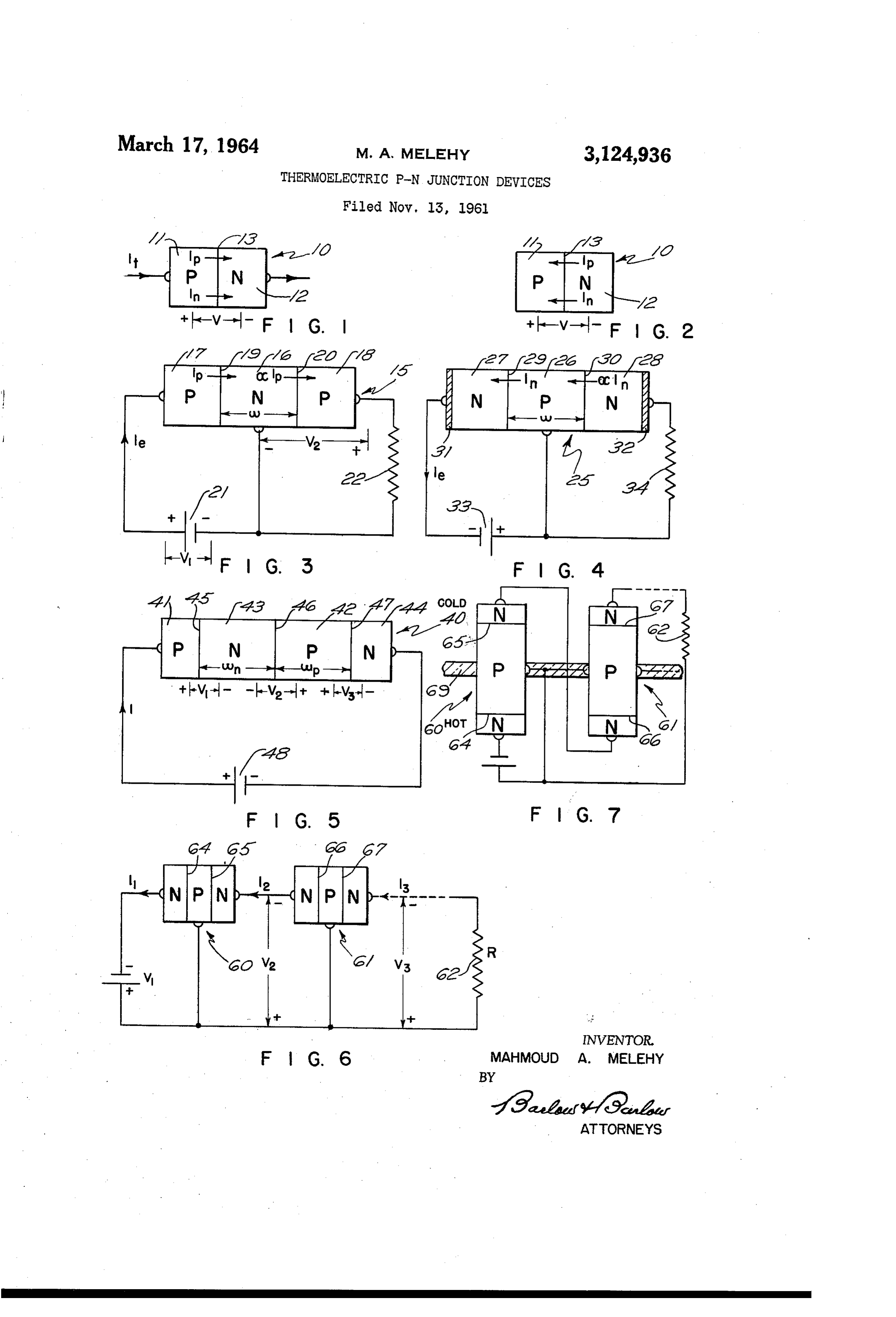
This invention relates to thermoelectric devices and An active element furnishes electrical energy rather than more particularly to single-crystal semiconductor ma dissipates it. Continuous supplying of electrical energy terials as thermoelectric elements. by an active element must be associated with the con Thermoelectric devices having non-single crystal junc O Version of some other form of energy to electrical energy. tions such as metal-to-metal, or metal-to-Semiconductor, For example, a battery converts chemical energy into or semiconductor-to-semiconductor junctions are Well electrical energy; and a D.C. generator converts mechani known. Such thermoelectric junctions are described in cal energy into electrical energy. numerous references such as the book entitled "Semi To understand the basis of heating and cooling in a conductor Thermoelements and Thermoelectric Cooling,' 5 p-n junction, let us refer to simple junctions as illustrated by A. F. Ioffe, published by Infosearch Limited, London, in FIGS. 1 and 2. In F.G. 1, there is shown a semi 1957; or the book entitled “Thermoelectricity,' by Paul conductor body 10 having a p-region 1 at its left-hand H. Egli, published by John Wiley and Sons, Inc., New end and an n-type region 12 at its right-hand end, these York, 1960. two regions being separated by a barrier junction 13. Let It is well known that a single-crystal semiconductor ma 20 us first consider, therefore, a forward biased p-n junction terial may have zones of alternately opposite conductivity as shown in FIG. 1. As is well known, when a p-n junc types. The boundary between each two neighboring tion is forward biased, its external behavior is determined Zones of opposite conductivity types is known as a p-n by the two types of minority carrier currents injected junction. The rectifying, amplifying and switching prop at the transition region or barrier 3, and the sum of erties of p-n junction devices are well known. These these two types of currents injected at the barrier is phenomena are described in many references Such as equal to the external current; i.e. It=I-I-I. This gen in an article entitled "The Theory of P-n Junctions in eral phenomenon is described in an article entitled “The Semiconductors and P-n Junction Transistors,' by Wil Theory of P-N Junctions in Semiconductors and P-N liam Shockley, appearing at page 335 of the Bell System Junction Transistors,” by William Shockley, appearing at Technical Journal for July, 1949, volume 28, No. 3, and 30 page 335 of the Bell System. Technical Journal for July, in an article entitled "P-N-P-N Transistor Switches,' by 1949, volume 28, No. 3. In this simple p-n junction, for J. L. Moll, M. Tanenbaum, J. M. Goldey and N. Holon ward biasing is associated with the injection of minority yak, Jr., appearing at page 1174 of the Proceedings of the carriers at the transition region, and this injection causes Institute of Radio Engineers for September, 1956, volume the density of minority carriers to rise on both sides of 44, No. 9. the transition above their respective thermal equilibrium In accordance with my invention, however, I provide values according to the formula two thermoelectric devices each of which consists of a single semiconductor crystal of three or four Zones of alternately opposite conductivity types; and appropriate where p and n are the densities of minority holes and circuits or circuit for each. 40 electrons respectively on either side of the transition re A better understanding of my invention may be had gion of the p-n junction; pn and n are the thermal equilib upon a reading of the following detailed description and rium values of p and n respectively; y is the forward an inspection of the drawings, in which: junction voltage; k is Boltzmann's constant; q is the FIG. 1 is a schematic illustration of a p-n junction magnitude of the electron charge and T is the absolute having a forward D.C. biasing voltage and forward in 45 junction temperature. Accordingly, as seen in F.G. 1, jection of minority carriers; the injected holes cross the boundary 13 from the p-type FIG. 2 is another schematic illustration showing an to the n-type region, and the electrons also cross the incomplete forward biased p-n junction with backward boundary 3 from the n-type to the p-type region, con injection of minority carriers; stituting an electron current in the same direction as FIG. 3 is a schematic illustration of a two-junction p-n-p 50 that of the hole current. Both currents are in the same thermoelectric device; -direction as the voltage drop across the junction as may FIG. 4 is a similar schematic illustration of an n-p-n be observed in the schematic drawing. Thus in the transi thermoelectric device with a modified heat conductor de tion region or barrier there is a dissipation of electrical Vice; power equal to the product of the total injected minority FIG. 5 is a schematic illustration of a three-junction 55 carrier current times the forward junction voltage v. thermoelectric device; This power is converted into heat, and the junction must F.G. 6 is a schematic illustration of several identical n act as a heat source and may be called passive. p-n thermoelectric devices connected in cascade; and Under certain conditions, a p-n junction may be for FIG. 7 is a diagrammatic and schematic illustration of Ward biased and yet the total injected current at the a device constructed in accordance with the invention. 60 junction may be in the direction of the voltage rise across Before discussing the problem of heating or cooling in the junction, Referring now to FEG. 2, it will be seen a p-n junction, let us consider first passive and active ele that there is diagrammed at barrier 13 both hole and ments from the standpoint of energy conversion. It is electron currents flowing from the n-type to the p-type well known that the flow of a D.C. current in an element region. In such a case, it can be said that both types can be either in the direction of the voltage drop, or 65 of minority carriers are backwardly injected at the junc the voltage rise across the element. In the first case, tion. However, if it happens, as will be shown later, that the element is called passive. Linear and non-linear re the p-n junction has one type of carriers injected forward sistors are passive elements. If a D.C. current passes ly and the other backwardly, then the direction of the through a passive element, all the electrical energy de net algebraic sum of both currents will determine whether livered to the element is converted into heat energy if 70 the injection is forward or backward. For example, if the temperature does not get too high. The rate at It is backwardly injected and is forwardly injected, which heat energy is generated by the element is simply and I). In then the total injected current will actually
Page 3
be backwardly injected. On the other hand, if I<In be a forwardly injected current. Such type of injection, then the net current is forwardly injected at the junction. as discussed earlier, tends to decrease the cooling effect In the case of junction 13 of FIG. 2, each of the two types caused by the hole current backwardly injected at junc of minority carrier currents and their sum are injected tion 20. Therefore, for best cooling at junction. 20, the backwardly; i.e. in the direction of the voltage rise across electron current injected at junction 26 must be reduced as the junction, then, as explained earlier, junction 3 is much as possible. This can be simply done by making the an active junction, which actually is furnishing electrical conductivity of zone 8 much higher than that of Zone 6. power. This power is simply equal to the product of In F.G. 4, I have shown another semiconductor body the total current injected at junction 13 and the junction 25 having a central p-type region 26 and two n-regions voltage (which is a rise in the direction of the total cur O 27 and 28. Region 27 is separated from region 26 by rent injected at barrier 13). Since there are no mechani a barrier junction 29, while region 28 is separated from cal or chemical changes in junction 13, it follows from region 26 by barrier junction 30. Suitably affixed to the conservation of energy principle that the junction the outer ends of the n-type regions 27 and 23 are metallic temperature must drop allowing heat energy to flow to the disks 3 and 32 which are affixed ohmically to these junction from its neighborhood. Thus junction 3 will 5 regions by welding or other suitable means, and to these act as a heat sink and the thermal energy will be con metalic disks ohmic connections are made, the negative verted there into electrical energy. The rate at which pole of a battery 33 being connected to plate 3: while heat energy is converted into electrical energy is simply the positive pole of battery 33 is connected to the p-type equal to the product of the net backwardly injected cur region 26 as well as to one end of a resistance 34, the rent at junction 3 and the forward junction voltage, 20 other end of which is connected to a metallic disk 32 I shall describe next two complete devices each of that is affixed ohmically to region 28. This particular which has one active junction of the sort just discussed. semiconductor device is identical in operation to that just Referring now to FIG. 3, there is shown a semiconduc described in connection with F.G. 3. The only difference tor body 5 including a central n-type region 16 and that exists here is that the type of regions has been p-type regions 7 and 3 at the left- and right-hand ends 25 changed, and accordingly the battery voltage has been thereof. The p-type region 7 is separated from the reversed to make junction 29 forward biased. Additional n-type region 6 by a barrier junction 9 and the p-type ly, the metailic disks which are physically attached to region 8 is separated from the n-type region 16 by a regions 27 and 28 serve as heat conductors as well as elec barrier junction 2. Ohmic connections are made to each trical conductors, and can also be used for the device of of the p-type and n-type regions, and the positive pole 30 FG, 3.
of a battery or D.C. source 2 is connected to the p-type Referring now to FIG. 5, there is shown therein a region .7, the negative pole of battery 2E being connected three-junction thermoelectric device having a semicon to the n-type region 6 and to one end of the resistance ductor body generally indicated 43 and having a pair of 22, while the other end of the resistance 22 is connected p-type regions 4A and 42 and a pair of n-type regions 43 to the p-type region i8. For reasons which will be pres and 44 in a p-n-p-n type of arrangement. Between re ently more fully discussed, the conductivity of the p-type ions 4 and 43 is a barrier junction 45, and between re region i7 must be much higher than that of the n-type gions 42 and 43 is a barrier junction 46, while between region 16, and the conductivity of the p-type region 18 the regions 42 and 44 there is a barrier region 47. Ohmic must similarly be much higher than that of the n-type connections are made to regions 48 and 44 by Suitable region 6. Additionally, the width w of the n-type re 40 wires to a battery 48. The operation of this device is gion 6 must be much less than the diffusion length for similar in some respects to that previously discussed, and minority carriers in that zone. In order to have a useful here the conductivity of region 4A is much higher than and practical device with the width of the n-type Zone that of region 43. Similarly the conductivity of region E6 as large as possible, materials must be chosen or 44 is much higher than that of region 42. Also the width developed for which the diffusion length is as large as of region 43 w is much less than the diffusion length possible. It will further be noted in FEG. 3 that junction Lp for minority holes in zone 43, and the width w of 19 is connected to the circuit in a fashion whereby the Zone 42 is much less than the diffusion iength L for junction is forward biased and an appropriate resistance minority electrons in zone 42. With a D.C. source con 22 is connected between the regions 6 and 18 which sisting of a battery 48 connected to the device as shown, controls the power furnished by junction 20, whose gen then both junctions 45 and 47 will be forward biased. It erated electrical power is substantially equal to the power accordingly follows that almost only holes will be injected dissipated in resistance 22. In operation, the hole current inwardly at junction 45 and only electrons will be injected at junction 9 is almost the only current injected if the inWardly at junction 47. Thus, just to the right of junc conductivity of zone 17 is much higher than that of 6. tion 45 the density of minority holes rises far above its Accordingly, if I is the hole current and I is the input 3 5 thermal equilibrium value, and this situation will be main current, then Iesi, If the width w of the n-type zone tained throughout Zone 43 since w is much less than the 16 is much less than the diffusion length L for minority diffusion length for minority carriers in zone 43. Simi holes in the Zone 6, then a large portion CI of the hole larly, the density of minority electrons will be far above current I injected at junction 19 will arrive at junction their thermal equilibrium value just to the left of junc 20; where c. is a fraction very nearly equal to unity. 60 tion 47, and this situation will be maintained throughout Furthermore, the density of minority holes just on the Zone 42. Thus, junction 46 must also be forward biased. left of junction 26 as viewed in the drawing will be much Since at junction 46 the hole current as well as the elec higher than its thermal equilibrium value. Thus, junc tron Current is along the direction from zone 43 to 42, tion 20 will be forward biased with a voltage v2 whose i.e. along the voltage rise across the junction, each of the polarity is as indicated in FIG. 3. Since the direction 65 two currents is injected backwardly in a forward biased of the whole current or is along the voltage rise across p-n junction. Hence, junction 46 is an active junction junction 20, then cI is a backwardly injected current in and will act as a heat sink. It will also be noticed that a forward biased junction, and as explained above, this the other two forward biased junctions 45 and 47 act as junction 20 must accordingly cool off. Because junction heat Sources, since both junctions are forward biased and 20 is forward biased, there will be an injection of minority 70 minority carriers are injected forwardly at each junction. electrons into region E8 from left to right as viewed in If the impurity concentration in zones 42 and 43 are uni the drawing, and it follows that the electron current will form, and if the three junction temperatures are the same, have the direction from right to left as viewed in the it can be shown that under optimum design conditions the drawing, which is in the direction of the voltage drop rate at which heat energy is pumped from junction 46 across junction. 20. Therefore, the electron current will 75 to junctions 45 and 47 is less but very nearly equal to
Page 4
the power furnished by battery 48, as may be seen from simple analysis neglects the heat leaking between the hot the following formula: and cold junctions.
m= (1-8) 100 FIGURE 7 shows a practical arrangement of the cas where caded semiconductors schematically illustrated in FEG Ö=2(wnw/LLI1/1n (I/Is) URE 6. Here they are physically arranged with the and cold junctions on one side of the insulating material 69 and the hot junctions on the other side thereof. This n: the percentage of the rate of heat energy pumped out heat is "generated on one side and “absorbed' on the of junction 46 to the power furnished by the battery; other. In this fashion we therefore have the “Cold re I: the battery current; O gion at the upper half of FiGURE 7 and the “Hot re Is: the reverse saturation current of junction 46 if the gion at the lower half of said FIGURE 7. A similar ar diffusion lengths for minority holes in Zone 43 and rangement can be made for p-n-p devices. minority electrons in Zone 42 were win and we re I claim:
spectively; 1. A thermoelectric device comprising a semiconductor L: the diffusion length for minority electrons in zone 42;
body of alternate opposite conductivity types with at
L: the diffusion length for minority holes in zone 43;least one active p-n junction and at least one passive p-n w: the width of the n-type Zone 43; junction forming inner and outer regions, the outer re w: the width of the p-type Zone 42. gions having higher conductivity than the inner region, It is apparent that in can be made as close to 100% the width of the inner region being much less than the as possible by reducing (wn/L) and (W/L) simul 20 diffusion length for minority carriers in said inner region taneously, and by selecting the proper materials. with distance between the said p-n junctions being sufi Referring now to FIG. 6, I have shown a circuit for ciently large so that the heat conduction between the cascading two or more two-junction thermoelectric de junctions is small.
vices of the n-p-n type. p-n-p devices can be connected 2. A thermoelectric device as in claim 1 wherein the identically with the battery polarity reversed. For sim 25 diffusion length for minority carriers in the inner region plicity, the figure shows only two devices 60 and 61. is on the order of at least 1500 microns. This circuit possesses some useful properties. With the 3. A thermoelectric device as in claim 1 wherein the specification described above that the (middle) p-region central region is made up of N and P type material. in each device is much shorter than the diffusion length 4. A thermoelectric device as in claim 1 wherein the for minority electrons, it is well known from the tran 30 central region is made up of N type material. sistor theory that the following relation exists 5. A thermoelectric device as in claim 1 wherein the central region is made up of P type material.
Islesla 6. A thermoelectric device comprising a body of semi
Also for certain values the load resistance R, v, v' and conductor material with adjacent layers being of opposite v will be described by conductivity types forming a plurality of p-n junctions, Said device including spaced outer layers and at least one interior base layer, a source of D.C. voltage connected where C is a constant less than, but nearly equal to, unity.
between the interior base layer and one outer layer, a load device connected between said other outer layer
Consider now the power generated or dissipated at 40 and said interior base layer, the p-n junctions being for every junction: Wardly biased so that there is a backward injection of Electrical power dissipated at junction 64=v (a pas minority carriers at the p-n junction adjacent the said sive junction) other outer layer connected to said load device. Electrical power dissipated at junction 66=vsy (IC 45 device 7. A thermoelectric device comprising a semiconductor a passive junction) comprising successive layers with adjacent layers Electrical power generated at junction 65=vIsvIC being of opposite conductivity types forming at least three an active junction) p-n junctions, said device including two outer layers of Electrical power generated at junction 67-yasyIC2 opposite conductivity type and two interior layers of op
posite conductivity type, a source of D.C. voltage con
Therefore, by means of the shown circuit, it is possible nected between the outer layers, said p-n junctions being to use a battery which furnishes a power (vi) to gen forwardly biased, the width of the interior N and Players erate cooling at a rate equal to v1.I (C-C) s211. Si being greater than the diffusion length for minority car multaneously, heat is generated at the junctions at a rate riers whereby the p-n junctions between the interior layers forms a heat sink.
equal to v1.I (1--C) s2v I. Also at the load resistance
R heat is generated at the rate of about vC2. This References (Cited in the file of this patent means that the rate at which heat is generated at the junctions and the load is equal to v1.1 (1--C--C2) s3y I Volker: Transactions of the Australian Institute of with a battery only furnishing a power of (VI). This Refrigeration Incorporated, February 1960, pages 13-18.
Provenance
- Collection
- Cited prior art
- Original PDF
- patentimages.storage.googleapis.com →
- Pages
- 4
- Method
- pdftotext (the PDF's own text layer) + pdftoppm 300dpi page scans
- Source
- Google Patents bibliographic record
- Granted
- 1964-03-17
- Transcribed from
- patentimages.storage.googleapis.com →