patent · US2780765
Solar energy converting apparatus
5 February 1957
Page 1
Drawing sheet — no readable text.
Page 2
United States Patent Office 2,780,765 atterated Feb. 5, 1957
However, it has been found that such a device is 2,780,765 particularly well suited for this purpose since a battery serves as a load whose resistance varies with charging
SOLAR ENERGY CONVERTING APPARATUS current in a manner corresponding to the resistance 5 variations of a p-n junction under the influence of incident
Daryl M. Chapin, Basking Ridge, Calvin S. Fuer, Chat radiation whereby the device is working into a well ham, and Gerald L. Pearson, Bernards Township, matched load over a wide range of incident light values. Somerset County, N. J., assignors to Ball Telepiele
Laboratories, incorporated, New York, N. Y., a cor There are several factors which in the past have poration of New York militated against high efficiencies in the use of a semi 0 conductive device including a p-n junction as a converter
Application March 5, 1954, Serial No. 414,273 of solar radiation. First, the usual semiconductive surface 12 Claims. (C. 320-2) tends to reflect a large fraction of the incident radiation, thereby reducing the radiation available for conversion.
Additionally, the recombination of electron-hole pairs
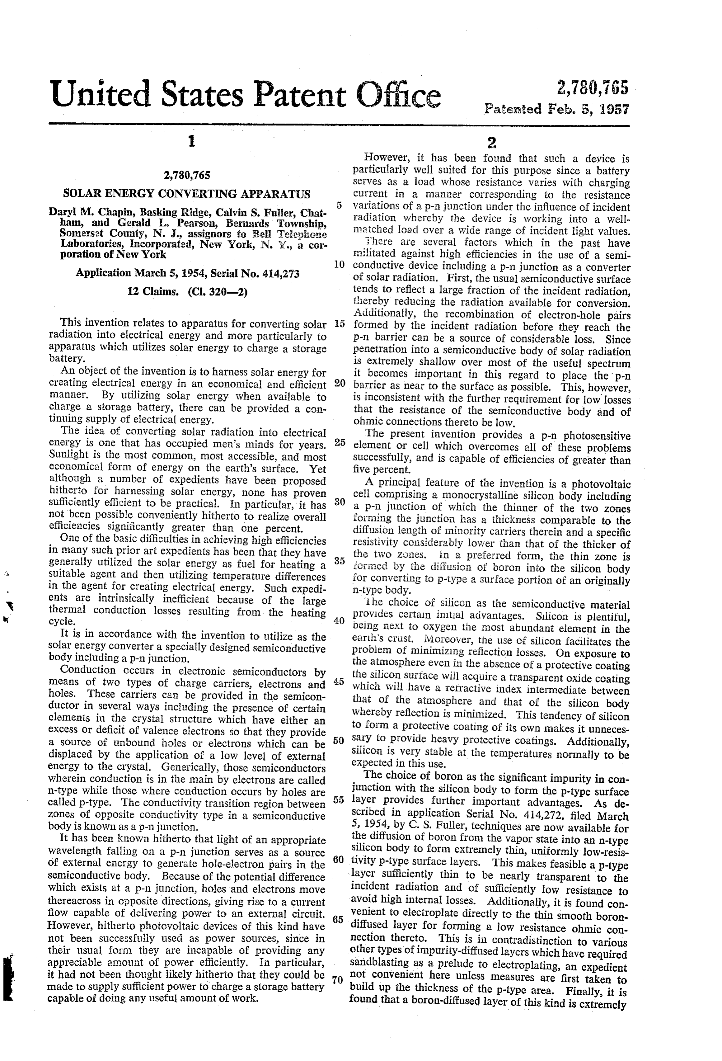
This invention relates to apparatus for converting solar 5 formed by the incident radiation before they reach the radiation into electrical energy and more particularly to p-n barrier can be a source of considerable loss. Since apparatus which utilizes solar energy to charge a storage penetration into a semiconductive body of solar radiation battery. is extremely shallow over most of the useful spectrum An object of the invention is to harness solar energy for it becomes important in this regard to place the p-n creating electrical energy in an economical and efficient 20 barrier as near to the surface as possible. This, however, manner. By utilizing solar energy when available to is inconsistent with the further requirement for low losses charge a storage battery, there can be provided a con that the resistance of the semiconductive body and of tinuing supply of electrical energy. ohmic connections thereto be low. The idea of converting solar radiation into electrical The present invention provides a p-n photosensitive energy is one that has occupied men's minds for years. 25 element or cell which overcomes all of these problems Sunlight is the most common, most accessible, and most Successfully, and is capable of efficiencies of greater than economical form of energy on the earth's surface. Yet five percent.
although a number of expedients have been proposed A principal feature of the invention is a photovoltaic hitherto for harnessing solar energy, none has proven cell comprising a monocrystalline silicon body including Sufficiently efficient to be practical. in particular, it has 30 a p-n junction of which the thinner of the two zones not been possible conveniently hitherto to realize overall fortning the junction has a thickness comparable to the efficiencies significantly greater than one percent. diffusion length of minority carriers therein and a specific One of the basic difficulties in achieving high efficiencies in many such prior art expedients has been that they have 35 resistivity considerably lower than that of the thicker of the two Zones, in a preferred form, the thin Zone is generally utilized the solar energy as fuel for heating a formed by the diffusion of boron into the silicon body Suitable agent and then utilizing temperature differences for converting to p-type a surface portion of an originally in the agent for creating electrical energy. Such expedi n-type body.
ents are intrinsically inefficient because of the large i he choice of silicon as the semiconductive material thermal cycle.
conduction losses resulting from the heating 40 provides certain initial advantages. Silicon is plentiful, It is in accordance with the invention to utilize as the being next to OXygen the most abundant element in the Solar energy converter a specially designed semiconductive earth's Crust. ivoreover, the use of silicon facilitates the body including a p-n junction. problem of minimizing reflection losses. On exposure to Conduction occurs in electronic semiconductors by the atmosphere even in the absence of a protective coating the silicon Surface will acquire a transparent oxide coating means of two types of charge carriers, electrons and 45 which holes. These carriers can be provided in the semicon will have a refractive index intermediate between ductor in several ways including the presence of certain that of the atmosphere and that of the silicon body elements in the crystal structure which have either an Whereby reflection is minimized. This tendency of silicon excess or deficit of valence electrons so that they provide 50 to form a protective coating of its own makes it unneces Sary to provide heavy protective coatings. Additionally, a source of unbound holes or electrons which can be displaced by the application of a low level of external silicon is very stable at the temperatures normally to be expected in this use.
energy to the crystal. Generically, those semiconductors wherein conduction is in the main by electrons are called The choice of boron as the significant impurity in con n-type while those where conduction occurs by holes are junction with the silicon body to form the p-type surface called p-type. The conductivity transition region between layer provides further important advantages. As de zones of opposite conductivity type in a semiconductive scribed in application Serial No. 414,272, filed March body is known as a p-n junction. 5, 1954, by C. S. Fuller, techniques are now available for It has been known hitherto that light of an appropriate the diffusion of boron from the vapor state into an n-type wavelength falling on a p-n junction serves as a source silicon body to form extremely thin, uniformly low-resis of external energy to generate hole-electron pairs in the 60 tivity p-type surface layers. This makes feasible a p-type semiconductive body. Because of the potential difference layer sufficiently thin to be nearly transparent to the which exists at a p-n junction, holes and electrons move incident radiation and of sufficiently low resistance to thereacross in opposite directions, giving rise to a current avoid high internal losses. Additionally, it is found con flow capable of delivering power to an external circuit. 65 venient to electroplate directly to the thin smooth boron However, hitherto photovoltaic devices of this kind have diffused layer for forming a low resistance ohmic con not been successfully used as power sources, since in nection thereto. This is in contradistinction to various their usual form they are incapable of providing any other types of impurity-diffused layers which have required appreciable amount of power efficiently. In particular, Sandblasting as a prelude to electroplating, an expedient it had not been thought likely hitherto that they could be not convenient here unless measures are first taken to made to supply sufficient power to charge a storage battery 70 build up the thickness of the p-type area. Finally, it is capable of doing any useful amount of work. found that a boron-diffused layer of this kind is extremely
Page 3
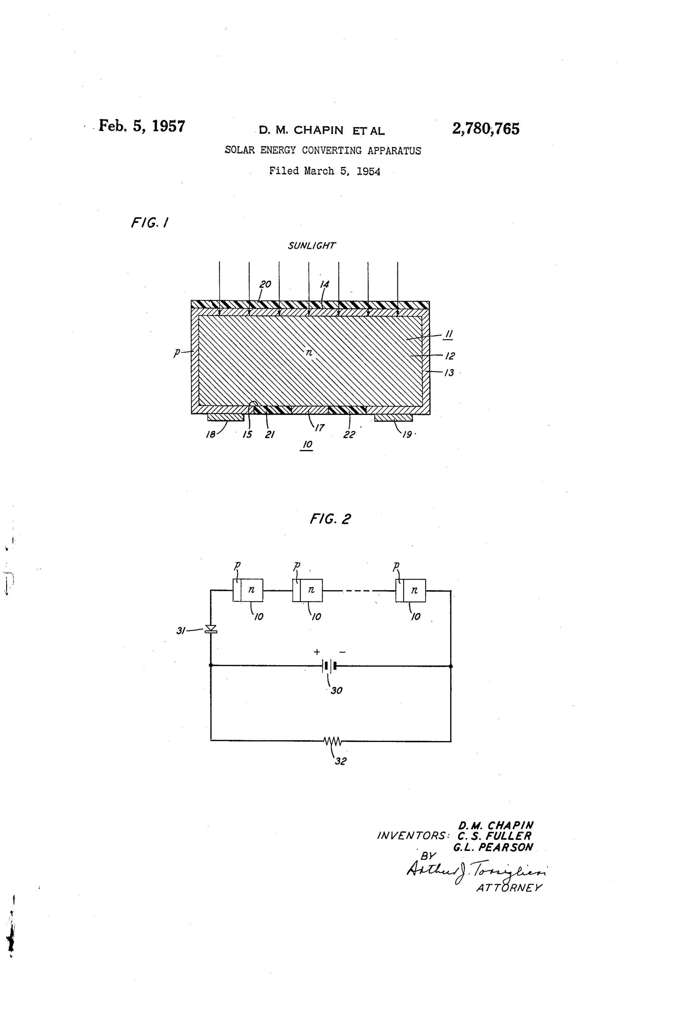
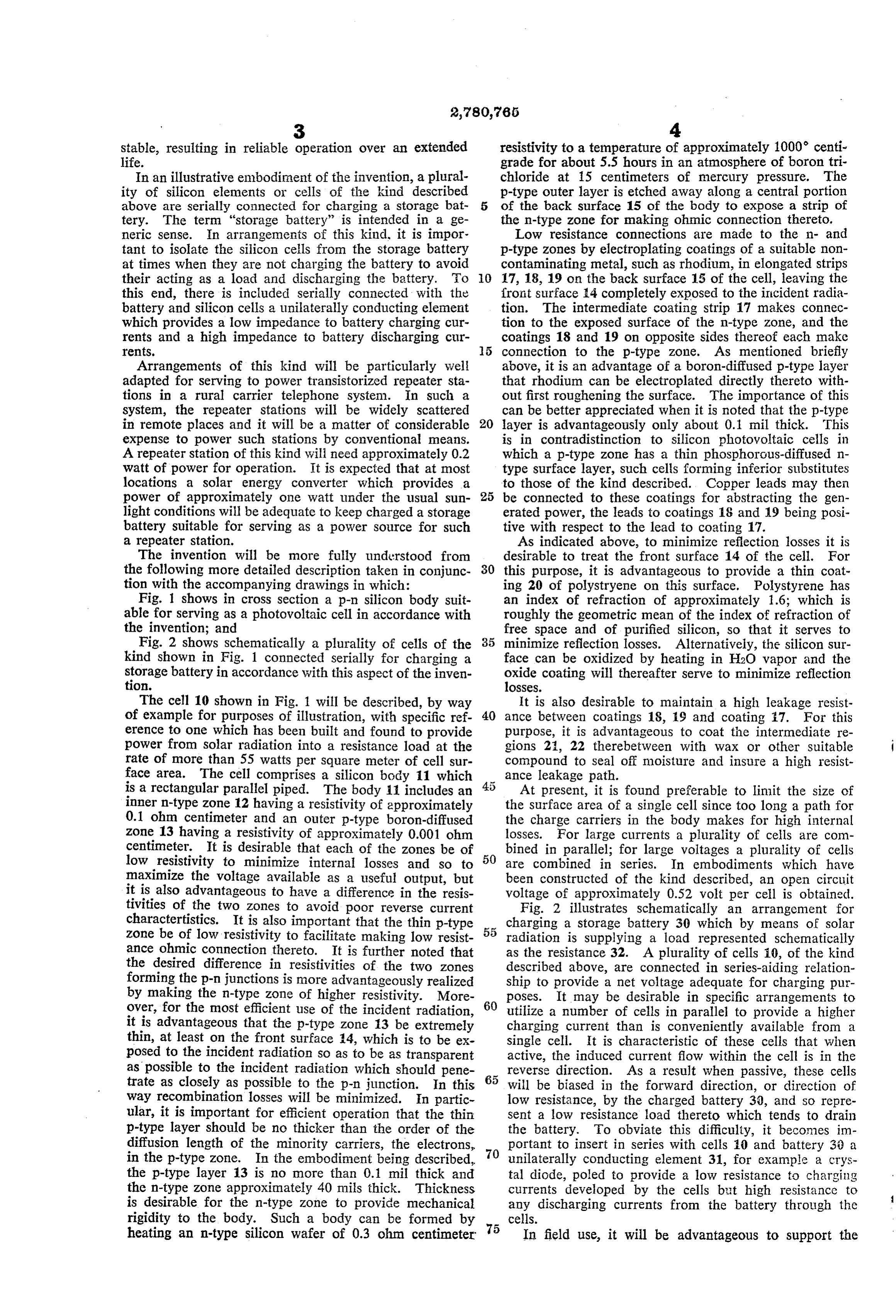
stable, resulting in reliable operation over an extended resistivity to a temperature of approximately 1000 centi life. grade for about 5.5 hours in an atmosphere of boron tri In an illustrative embodiment of the invention, a plural chloride at 15 centimeters of mercury pressure. The ity of silicon elements or cells of the kind described p-type outer layer is etched away along a central portion above are serially connected for charging a storage bat of the back surface 15 of the body to expose a strip of tery. The term "storage battery' is intended in a ge the n-type zone for making ohmic connection thereto. neric sense. In arrangements of this kind, it is impor Low resistance connections are made to the n- and tant to isolate the silicon cells from the storage battery p-type zones by electroplating coatings of a suitable non at times when they are not charging the battery to avoid contaminating metal, such as rhodium, in elongated strips their acting as a load and discharging the battery. To O 17, 18, 19 on the back surface 15 of the cell, leaving the this end, there is included serially connected with the front surface 4 completely exposed to the incident radia battery and silicon cells a unilaterally conducting element tion. The intermediate coating strip 17 makes connec which provides a low impedance to battery charging cur tion to the exposed surface of the n-type Zone, and the rents and a high impedance to battery discharging cur coatings 18 and 19 on opposite sides thereof each make rents. connection to the p-type Zone. As mentioned briefly Arrangements of this kind will be particularly well above, it is an advantage of a boron-diffused p-type layer adapted for serving to power transistorized repeater sta that rhodium can be electroplated directly thereto with tions in a rural carrier telephone system. In such a out first roughening the surface. The importance of this system, the repeater stations will be widely scattered can be better appreciated when it is noted that the p-type in remote places and it will be a matter of considerable 20 layer is advantageously only about 0.1 mill thick. This expense to power such stations by conventional means. is in contradistinction to silicon photovoltaic cells in A repeater station of this kind will need approximately 0.2 which a p-type zone has a thin phosphorous-diffused n watt of power for operation. It is expected that at most type surface layer, such cells forming inferior substitutes locations a solar energy converter which provides a to those of the kind described. Copper leads may then power of approximately one watt under the usual sun 25 be connected to these coatings for abstracting the gen light conditions will be adequate to keep charged a storage erated power, the leads to coatings 18 and 19 being posi battery suitable for serving as a power source for such tive with respect to the lead to coating 17. a repeater station. As indicated above, to minimize reflection losses it is The invention will be more fully understood from desirable to treat the front surface 14 of the cell. For the following more detailed description taken in conjunc 30 this purpose, it is advantageous to provide a thin coat tion with the accompanying drawings in which: ing 20 of polystryene on this surface. Polystyrene has Fig. I shows in cross section a p-n silicon body suit an index of refraction of approximately 1.6; which is able for serving as a photovoltaic cell in accordance with roughly the geometric mean of the index of refraction of the invention; and free space and of purified silicon, so that it serves to Fig. 2 shows schematically a plurality of cells of the 35 minimize reflection losses. Alternatively, the silicon sur kind shown in Fig. 1 connected serially for charging a face can be oxidized by heating in H2O vapor and the storage battery in accordance with this aspect of the inven oxide coating will thereafter serve to minimize reflection tion. losses.
The cell 10 shown in Fig. 1 will be described, by way It is also desirable to maintain a high leakage resist of example for purposes of illustration, with specific ref 40 ance between coatings 18, 19 and coating 17. For this erence to one which has been built and found to provide purpose, it is advantageous to coat the intermediate re power from Solar radiation into a resistance load at the gions 2:, 22 therebetween with wax or other suitable rate of more than 55 watts per square meter of cell sur compound to Seal off moisture and insure a high resist face area. The cell comprises a silicon body 11 which ance leakage path.
is a rectangular parallel piped. The body 11 includes an At present, it is found preferable to limit the size of inner n-type Zone 12 having a resistivity of approximately the Surface area of a single cell since too long a path for 0.1 ohm centimeter and an outer p-type boron-diffused the charge carriers in the body makes for high internal Zone 13 having a resistivity of approximately 0.001 ohm losses. For large currents a plurality of cells are com centimeter. It is desirable that each of the zones be of 50 bined in parallel; for large voltages a plurality of cells low resistivity to minimize internal losses and so to are combined in series. In embodiments which have maximize the voltage available as a useful output, but been constructed of the kind described, an open circuit it is also advantageous to have a difference in the resis voltage of approximately 0.52 volt per cell is obtained. tivities of the two zones to avoid poor reverse current Fig. 2 illustrates schematically an arrangement for charactertistics. It is also important that the thin p-type 55 charging a storage battery 30 which by means of solar Zone be of low resistivity to facilitate making low resist radiation is supplying a load represented schematically ance ohmic connection thereto. It is further noted that as the resistance 32. A plurality of cells i0, of the kind the desired difference in resistivities of the two zones described above, are connected in series-aiding relation forming the p-n junctions is more advantageously realized ship to provide a net voltage adequate for charging pur by making the n-type Zone of higher resistivity. More 60 poses. It may be desirable in specific arrangements to over, for the most efficient use of the incident radiation, utilize a number of cells in parallel to provide a higher it is advantageous that the p-type zone 13 be extremely charging current than is conveniently available from a thin, at least on the front surface 14, which is to be ex Single cell. It is characteristic of these cells that when posed to the incident radiation so as to be as transparent active, the induced current flow within the cell is in the as possible to the incident radiation which should pene reverse direction. As a result when passive, these cells trate as closely as possible to the p-n junction. In this 65 will be biased in the forward direction, or direction of way recombination losses will be minimized. In partic low resistance, by the charged battery 30, and so repre ular, it is important for efficient operation that the thin Sent a low resistance load thereto which tends to drain p-type layer should be no thicker than the order of the the battery. To obviate this difficulty, it becomes im diffusion length of the minority carriers, the electrons, portant to insert in series with cells 10 and battery 3i) a in the p-type Zone. In the embodiment being described, 70 unilaterally conducting element 31, for example a crys the p-type layer 3 is no more than 0.1 mill thick and tal diode, poled to provide a low resistance to charging the n-type Zone approximately 40 mills thick. Thickness currents developed by the cells but high resistance to is desirable for the n-type Zone to provide mechanical any discharging currents from the battery through the rigidity to the body. Such a body can be formed by 75 cells.
heating an n-type silicon wafer of 0.3 ohm centimeter In field use, it will be advantageous to support the
Page 4
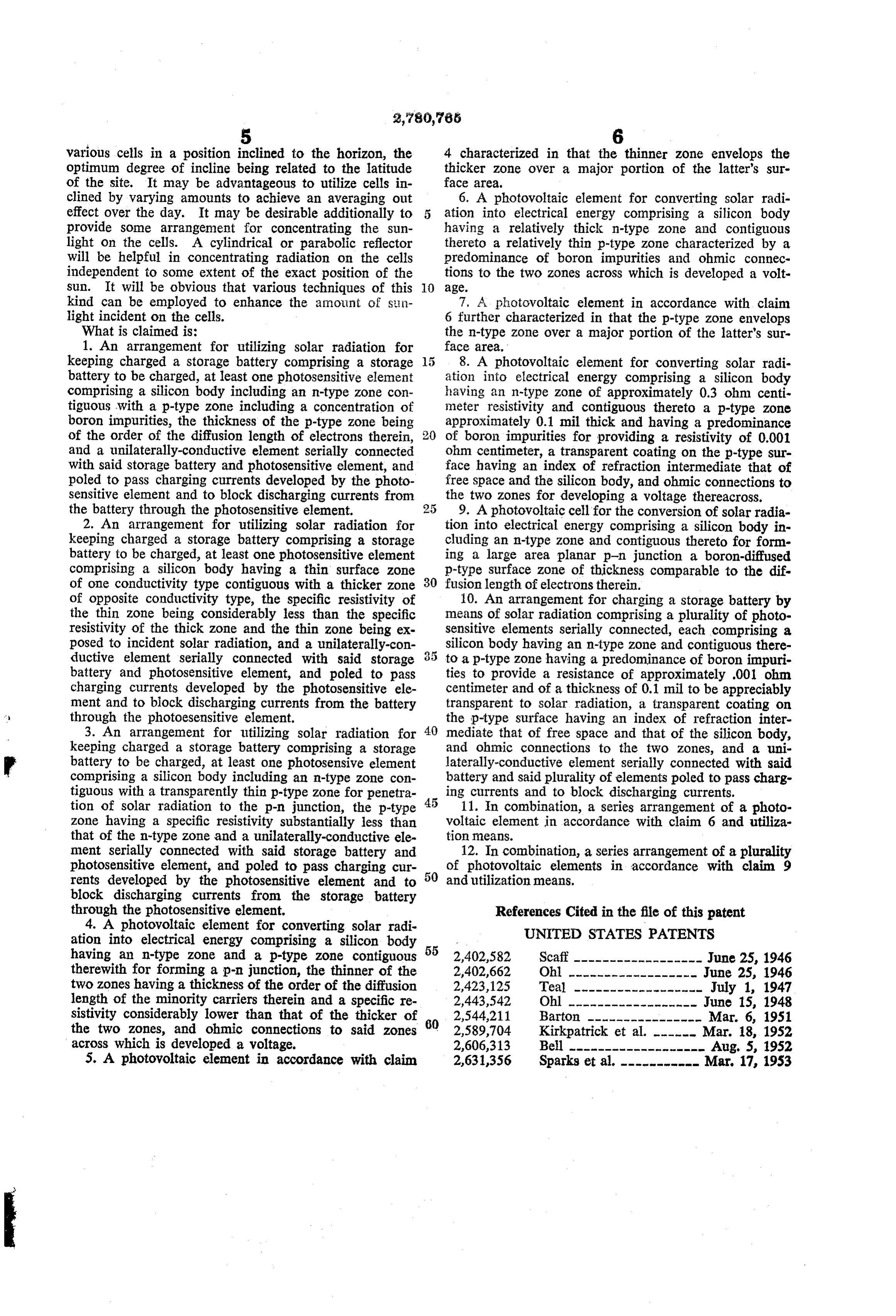
various cells in a position inclined to the horizon, the 4 characterized in that the thinner zone envelops the optimum degree of incline being related to the latitude thicker zone over a major portion of the latter's sur of the site. It may be advantageous to utilize cells in face area.
clined by varying amounts to achieve an averaging out 6. A photovoltaic element for converting solar radi effect over the day. It may be desirable additionally to 5 ation into electrical energy comprising a silicon body provide some arrangement for concentrating the sun having a relatively thick n-type zone and contiguous light on the cells. A cylindrical or parabolic reflector thereto a relatively thin p-type Zone characterized by a will be helpful in concentrating radiation on the cells predominance of boron impurities and ohmic connec independent to some extent of the exact position of the tions to the two zones across which is developed a volt Sun. It will be obvious that various techniques of this 10 age.
kind can be employed to enhance the amount of sin 7. A photovoltaic element in accordance with claim light incident on the cells. 6 further characterized in that the p-type zone envelops What is claimed is: the n-type Zone over a major portion of the latter's sur 1. An arrangement for utilizing solar radiation for face area.
keeping charged a storage battery comprising a storage 8. A photovoltaic element for converting solar radi battery to be charged, at least one photosensitive element ation into electrical energy comprising a silicon body comprising a silicon body including an n-type zone con having an n-type Zone of approximately 0.3 ohm centi tiguous with a p-type Zone including a concentration of meter resistivity and contiguous thereto a p-type zone boron impurities, the thickness of the p-type zone being approximately 0.1 mil thick and having a predominance of the order of the diffusion length of electrons therein, 20 of boron impurities for providing a resistivity of 0.001 and a unilaterally-conductive element serially connected ohm centimeter, a transparent coating on the p-type sur with said storage battery and photosensitive element, and face having an index of refraction intermediate that of poled to pass charging currents developed by the photo free space and the silicon body, and ohmic connections to sensitive element and to block discharging currents from the two Zones for developing a voltage thereacross. the battery through the photosensitive element. 25 9. A photovoltaic cell for the conversion of solar radia 2. An arrangement for utilizing solar radiation for tion into electrical energy comprising a silicon body in keeping charged a storage battery comprising a storage cluding an n-type Zone and contiguous thereto for form battery to be charged, at least one photosensitive element ing a large area planar p-n junction a boron-diffused comprising a silicon body having a thin surface zone p-type surface Zone of thickness comparable to the dif of one conductivity type contiguous with a thicker zone 30 fusion length of electrons therein. of opposite conductivity type, the specific resistivity of 10. An arrangement for charging a storage battery by the thin Zone being considerably less than the specific means of Solar radiation comprising a plurality of photo resistivity of the thick Zone and the thin zone being ex sensitive elements serially connected, each comprising a posed to incident solar radiation, and a unilaterally-con silicon body having an n-type Zone and contiguous there ductive element serially connected with said storage to a p-type Zone having a predominance of boron impuri battery and photosensitive element, and poled to pass ties to provide a resistance of approximately .001 ohm charging currents developed by the photosensitive ele centimeter and of a thickness of 0.1 mill to be appreciably ment and to block discharging currents from the battery fransparent to Solar radiation, a transparent coating on through the photoesensitive element. the p-type surface having an index of refraction inter 3. An arrangement for utilizing solar radiation for 40 mediate that of free space and that of the silicon body, keeping charged a storage battery comprising a storage and ohmic connections to the two zones, and a uni battery to be charged, at least one photosensive element laterally-conductive element serially connected with said comprising a silicon body including an n-type zone con battery and said plurality of elements poled to pass charg tiguous with a transparently thin p-type zone for penetra 45 ing currents and to block discharging currents. tion of solar radiation to the p-n junction, the p-type 11. In combination, a series arrangement of a photo Zone having a specific resistivity substantially less than voltaic element in accordance with claim 6 and utiliza that of the n-type Zone and a unilaterally-conductive ele tion means.
ment serially connected with said storage battery and 12. In combination, a series arrangement of a plurality photosensitive element, and poled to pass charging cur of photovoltaic elements in accordance with claim 9 rents developed by the photosensitive element and to and utilization means.
block discharging currents from the storage battery through the photosensitive element. References Cited in the file of this patent 4. A photovoltaic element for converting solar radi UNITED STATES PATENTS ation into electrical energy comprising a silicon body 55 having an n-type Zone and a p-type zone contiguous 2,402,582 Scaff------------------ June 25, 1946 therewith for forming a p-n junction, the thinner of the 2,402,662 Ohl ------------------ June 25, 1946 two zones having a thickness of the order of the diffusion
length of the minority carriers therein and a specific re2,443,542 Ohl ------------------ June 15, 1948 sistivity considerably lower than that of the thicker of 2,544,211 Barton ---------------- Mar. 6, 1951 the two zones, and ohmic connections to said zones 60 2,589,704 Kirkpatrick et al. ------ Mar. 18, 1952 across which is developed a voltage. 2,606,313 Bell ------------------- Aug. 5, 1952 5. A photovoltaic element in accordance with claim 2,631,356 Sparks et al. ----------- Mar, 17, 1953
Provenance
- Collection
- Cited prior art
- Original PDF
- patentimages.storage.googleapis.com →
- Filed
- 1954-03-05
- Pages
- 4
- Method
- pdftotext (the PDF's own text layer) + pdftoppm 300dpi page scans
- Source
- Google Patents bibliographic record
- Granted
- 1957-02-05
- Inventors
- Daryl M Chapin; Calvin S Fuller; Gerald L Pearson; Bell Telephone Laboratories Inc
- Transcribed from
- patentimages.storage.googleapis.com →