patent · US6323414
Heterostructure thermionic coolers
27 November 2001
Page 1 — bibliographic record
(12) United States Patent (10) Patent No.: US 6,323,414 B1 Shakouri et al. (45) Date of Patent: *Nov. 27, 2001
(54) HETEROSTRUCTURE THERMIONIC OTHER PUBLICATIONS
COOLERS
N. W. Ashcroft, et al., Solid State Physics, manual, 1976, pp.
(75) Inventors: Ali Shakouri; John E. Bowers, both of 318,319, 320-321, 362-363. No month and/or year pro Santa Barbara, CA (US) vided.
D. A. Broido et al., “Effect of Superlattice structure on the (73) Assignee: The Regents of the University of thermoelectric figure of merit:”, The American Physical California, Oakland, CA (US) Society (Physical Review B.), vol. 51, No. 19, May 15,
(*) Notice: Subject to any disclaimer, the term of this D. A. Broido et al., "Comment of Use of quantum well patent is extended or adjusted under 35 Superlattices to obtain high figure of merit from nonconven U.S.C. 154(b) by 0 days. tional thermoelectric materials”, Appl. Phys. Lett. 63, 3230 (1993), Applied Physics Letters, vol. 67, No. 8, Aug. 21,
This patent is Subject to a terminal dis- 1995, pp. 1170–1171.
claimer. D. A. Broido et al., “Thermoelectric figure or merit of quantum wire Superlattices”, Applied Physics Letters, July 3, (21) Appl. No.: 09/548,011 1995, vol. 67, No. 1, 100-102. (22) Filed: Apr. 12, 2000 (List continued on next page.) O O Primary Examiner Bruce F. Bell
Related U.S. Application Data ASSistant Examiner Thomas H Parsons (60) Continuation of application No. 09/280.284, filed on Mar. (74) Attorney, Agent, or Firm-Gates & Cooper LLP
application No. 08/767935, filed on Dec. 17, 1996, now Pat. (57) ABSTRACT No. 5,955,772. A heterostructure thermionic cooler and a method for mak (51) Int. Cl." ..................................................... H01L 35/30 ing thermionic coolers, employing a barrier layer of varying (52) U.S. Cl. ....................... 136/205; 252/62.3 T; 257/26; conduction bandedge for n-type material, or varying Valence 257/185; 257/191; 257/442; 257/443; 257/449; bandedge for p-type material, that is placed between two 257/467 layers of material. The barrier layer has a high enough (58) Field of Search ..................................... 136/203, 205 barrier for the cold side to only allow “hot” electrons, or 136/236.1, 238, 239, 240; 252/62.3 T. 257/467 electrons of high enough energy, across the barrier. The iss 191 196 26 442, 443 s 449 930. barrier layer is constructed to have an internal electric field s s s a s/s s s s 15 Such that the electrons that make it over the initial barrier are assisted in travel to the anode. Once electrons drop to the (56) References Cited energy level of the anode, they lose energy to the lattice, thus heating the lattice at the anode. The barrier height of the
4,353,081 10/1982 Allyn et al. .......................... 257/19 traveling in the reverse direction. 4,694,318 9/1987 Capasso et al. ....................... 257/21 5,955,772 9/1999 Shakouri et al. ..... ... 257/467 30 Claims, 5 Drawing Sheets
d 32 dA,
Page 2
OTHER PUBLICATIONS J. M. Houston, “Theoretical efficiency of the thermionic P. J. Lin-Chung, et al., “Thermoelectric figure of merit of energy converter”, Journal of Applied Phyics, vol. 30 No. 4, composite Superlattice Systems, Physical Review B (con Apr. 1959, pp. 481-487.
densed matter), vol. 51, No. 19, May 15, 1995, pp. 13244-8. L. W. Whitlow, et al., “Superlative applications to thermo A. J. Dekker, “Thermionic Emission”, McGraw-Hill Ency electricity”, Journal of Applied Physics, Nov. 1, 1995, vol., clopedia of Science & Technology, 6' Edition, 1987, vol. 78, No. 9, 5460-5466.
18, pp. 272-273. No month and/or year provided. G.D. Mahan, et al., “Thermoelectric devices using Semicon L. D. Hicks, et al., “Effect of quantum-well strucutres on the ductor quantum wells”, Journal of Applied Physics, vol. 76, thermoelectric figure of merit”, Physical Review B (con No. 3, Aug. 1, 1994, 1899–1901.
densed matter), vol. 47, No. 19, May 15, 1993, pp. G. D. Mahan, et al., “Thermionic refrigeration”, Journal of 12727-12731. Applied Physics, vol. 76, No. 7, Oct. 1, 1994, 4362–6. L. D. Hicks, et al. “Thermoelectric figure of merit of a Sofo, J. O., “Thermoelectric figure of merit of Superlattices”, one-dimensional conductor”, Physical Review B (con Applied Physics Letters, vol. 65, No. 21, Nov. 21, 1994, densed matter), vol. 47, No. 24, Jun. 15, 1993, 16631-4. 2690-2.
L. D. Hicks, et al. “Use of Quantum-well Superlattices to D. M. Rowe, et al., “Multiple Potential Barriers as a Possible obtain a high figure of merit from nonconventional thermo Mechanism to Increase the Seebeck Coefficient and Elec electric materials”, Applied Physics Letters, vol. 63, No. 23, trical Power Factor', Thirteenth International Conference on Dec. 6, 1993, 3230–2. Thermoelectrics, Kansas City, Mo. USA, Aug. 30-Sep. 1, L. D. Hicks, et al., Experimental study of the effect of 1994.
quantum-Well Structures on the thermoelectric figure of K. K. Ng, “Complete Guide to Semiconductor Devices.” merit, Physical Review B (condensed matter), vol. 53, No. McGraw-Hill, 1995, pp. 48-55. No month and/or year 16, R10493-6. No month and/or year provided. provided.
Page 3
Drawing sheet — no readable text.
Page 4
Drawing sheet — no readable text.
Page 5
Drawing sheet — no readable text.
Page 6
Drawing sheet — no readable text.
Page 7
Drawing sheet — no readable text.
Page 8
HETEROSTRUCTURE THERMONIC room temperature. By using proper materials and COOLERS geometries, efficient and Space conserving thermionic cooler elements which can reach lower temperatures are fabricated
This application is a continuation of and commonly in a cost-effective manner.
assigned patent application Ser. No. 09/280,284, filed Mar. The principles of the present invention comprise growing 29, 1999, entitled “METHOD FOR MAKING HETERO two Semiconductor layers. The Second layer has a variable STRUCTURE THERMIONIC COOLERS,” by Ali Shak conduction bandedge as a function of distance (for the case ouri et al.(now U.S. Pat. No. 6,060,331), which is a divi of electron transport) which has its maximum bigger than sional application of Ser. No. 08/767,935, filed Dec. 17, the first layer. Selective thermionic emission of high energy 1996, entitled “HETEROSTRUCTURE THERMIONIC carriers from cathode to anode (and Suppressing the reverse COOLERS,” by Ali Shakouri, et al., now U.S. Pat. No. current) will create a cold junction at the cathode and a hot 5,955,772 issued on Sep. 21, 1999. junction at the anode. This device will function at room temperature and below. Using the same device in contact
STATEMENT REGARDING FEDERALLY with a hot and cold bath will create a thermionic generator SPONSORED RESEARCH AND 15 which also works at room temperature and below.
DEVELOPMENT
One object of the present invention is to provide better
This invention was made with Government support under electronic cooler fabrication techniques. It is a further object Contract No. F49620-96-1-0349, awarded by the Air Force. of the invention to reduce electronic cooler fabrication costs. The Government has certain rights in this invention. It is a further object of the invention to make more efficient electronic coolers which reach lower temperatures.
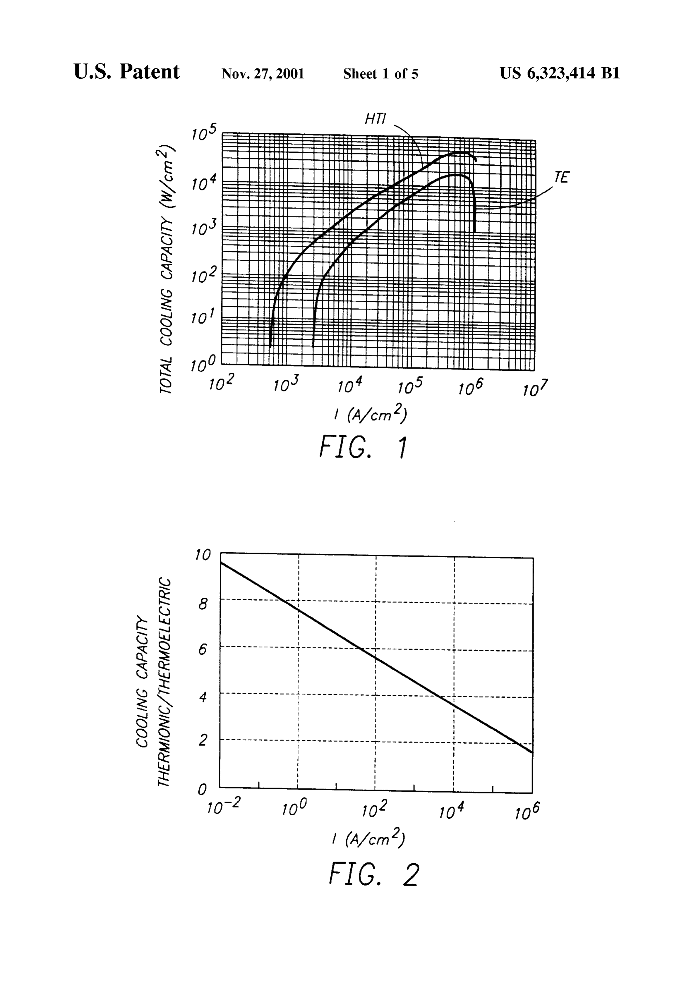
BACKGROUND OF THE INVENTION These and various other advantages and features of nov 1. Field of the Invention elty which characterize the invention are pointed out with This invention relates in general to electronic devices, and particularity in the claims annexed hereto and form a part more specifically to the first use of Semiconductor materials 25 hereof. However, for a better understanding of the invention, its advantages, and the objects obtained by its use, reference to fabricate thermionic coolers and generators. should be made to the drawings which form a further part 2. Description of Related Art hereof, and to accompanying descriptive matter, in which The use of electronics to transport heat to and away from there are illustrated and described Specific examples of an certain areas has expanded in recent years due to increased apparatus in accordance with the invention. packing densities and hostile environments. For cooling BRIEF DESCRIPTION OF THE DRAWINGS applications, thermoelectric coolers (TE Coolers) have been used to cool areas both in electronic and non-electronic Referring now to the drawings in which like reference applications. TE coolers are typically a p-type doped region numbers represent corresponding parts throughout: alternatively connected to an n-type doped region, which FIG. 1 shows the overall cooling power for thermionic creates cooling effects at one metal-doped region junction 35 devices and thermoelectric devices, and heating effects at the other metal-doped region junction, depending on the direction of the current through the device. theFIG.2 shows the ratio of the thermionic cooling term over Peltier cooling term as a function of current;
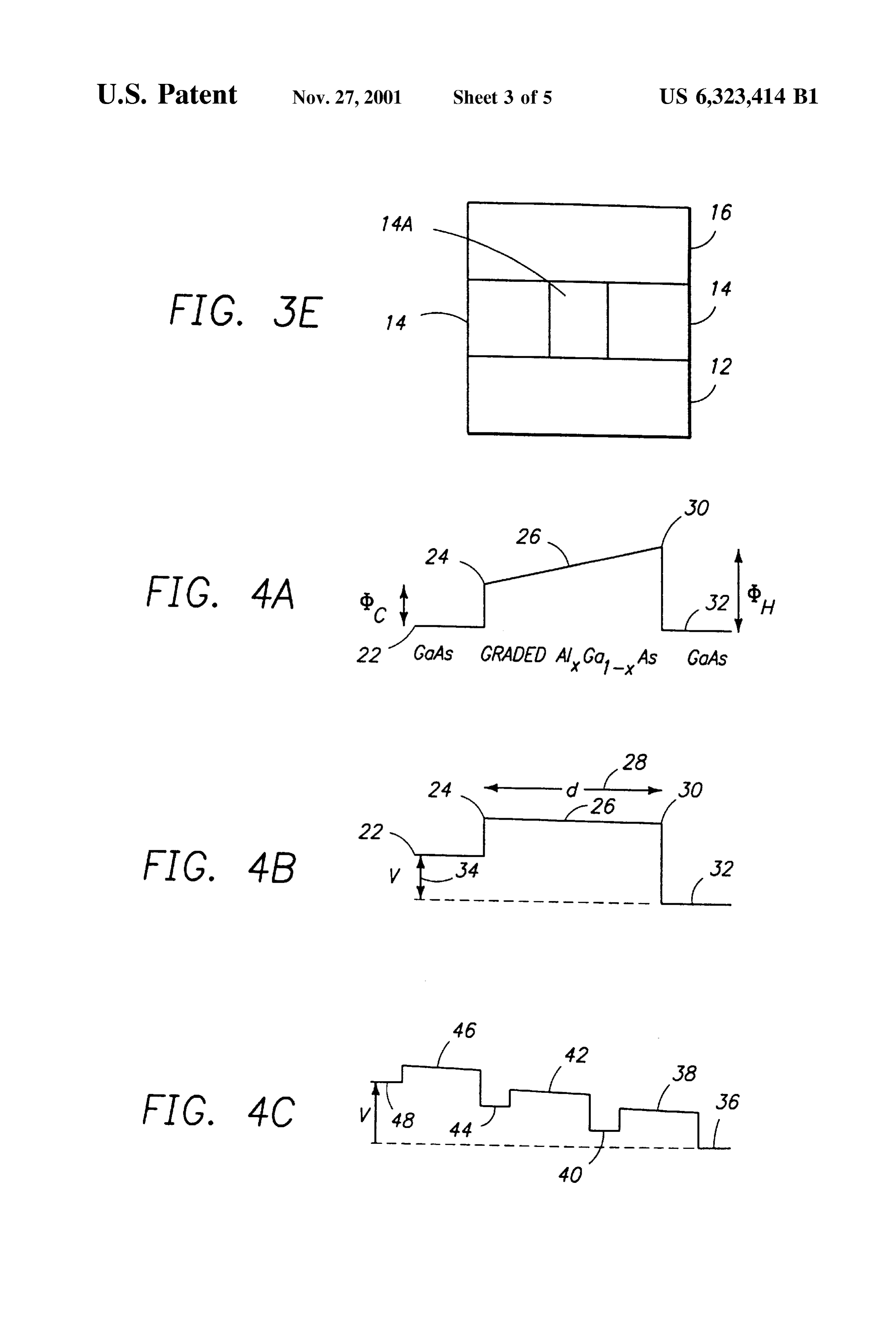
However, TE coolers are limited in their overall perfor FIGS. 3A-3E are diagrams of a first embodiment of the mance by the bulk properties of the materials used in the TE 40 present invention;
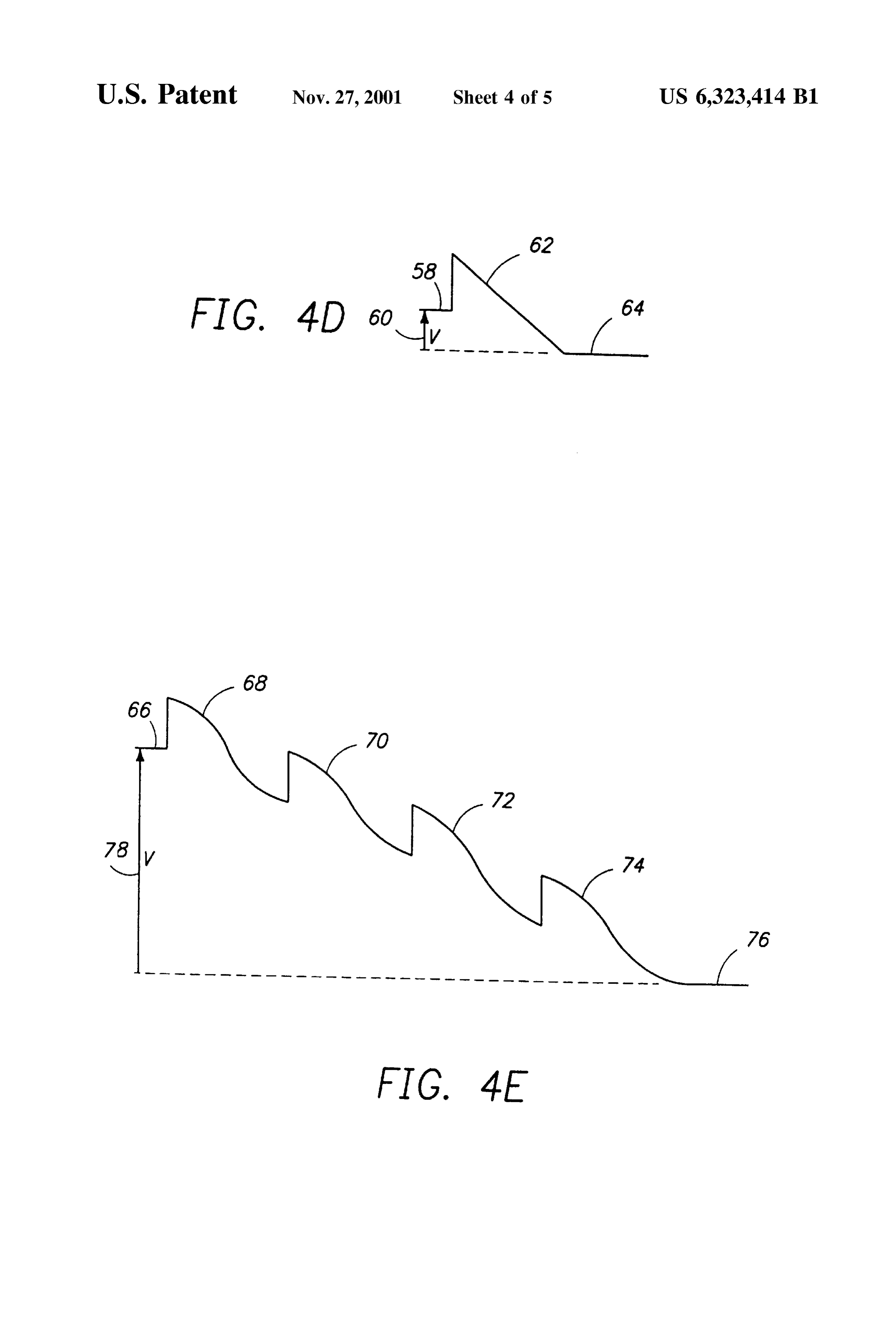
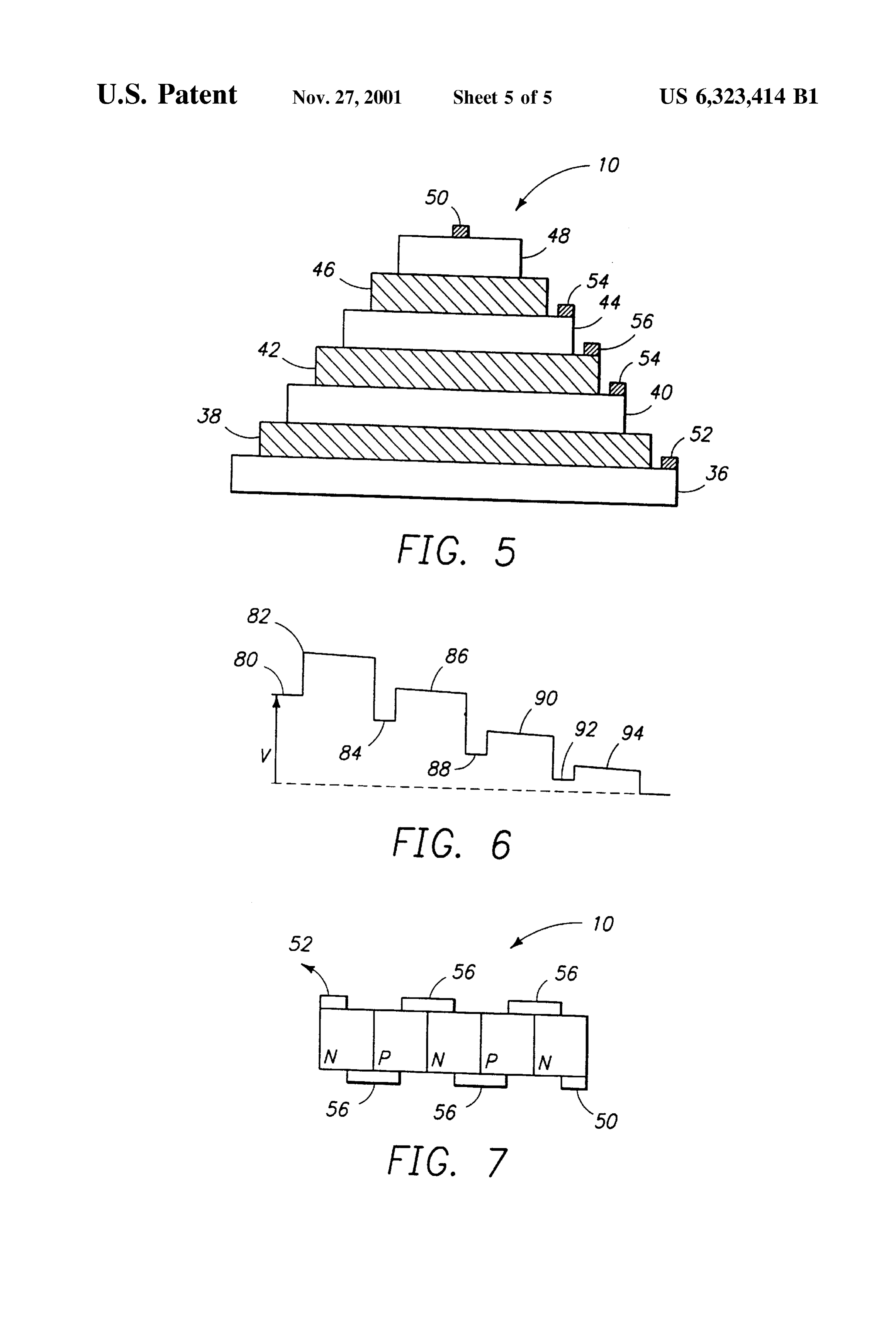
cooler. More efficient cooling is needed in many applica FIGS. 4A-4E are graphs of the conduction bandedge of tions. Reliability of assemblies of many elements is often not devices made using the present invention; sufficient for many high reliability designs. The cost of TE coolers has not plummeted at the same rate as other elec FIG. 5 shows an alternative structure for the device 10; tronic devices Such as transistor circuits, lasers and 45 FIG. 6 shows a cascaded device using Stages with differ detectors, because TE cooler elements are not fabricated ent bandedge discontinuities, and using high Volume planar integrated circuit technology. FIG. 7 shows a combination of n-doped and p-doped Further, TE coolers that can generate a large cooling effect devices as described in the present invention. tend to be large devices, typically 1 cmx1 cm or larger and DETAILED DESCRIPTION OF THE thus, are not acceptable in Small electronic devices. 50 INVENTION
It can be seen then that there is a need for better electronic Overview coolers. It can also be seen then that there is a need for better The present invention uses thermionic emission in Semi electronic cooler fabrication techniques. It can also be seen conductor heterostructures for heat pumping and cooling of that there is a need for low cost electronic coolers. It can also high power electronic and optoelectronic devices. These be seen that there is a need for more Space efficient electronic 55 integrated micro-coolers can improve the efficiency and coolers. It can also be seen that there is a need for more lifetime of electrical and optoelectronic components. The energy efficient electronic coolers. It can also be seen that thermionic coolers could also be used as an additional means there is a need for more reliable electronic coolers. It can for tuning temperature Sensitive devices. also be seen that there is a need for electronic coolers that The coolers that are commercially available are typically reach lower temperatures. 60 thermoelectric (TE) coolers, based on the Peltier effect at the SUMMARY OF THE INVENTION junction of two dissimilar materials. TE coolers use a materials bulk properties, Such as the Seebeck coefficient,
The present invention discloses a powerful and highly electrical and thermal conductivity, and are mostly based on productive Semiconductor thermionic cooler. Bismuth Telluride (Bi-Te) for room temperature applica The present invention minimizes the above-described 65 tions. The basis of the heterostructure thermionic (HTI) problems by using bandgap engineering and modulation cooler described here is to use bandstructure engineering to doping to fabricate Small thermionic coolers that operate at increase the cooling power and efficiency.
Page 9
Recent proposals to use quantum wells, quantum wires, The two branches are connected electrically in Series and and Superlattice Structures to increase the TE cooler figure of thermally in parallel. When the current is flowing from n to merit can be divided into two categories. The first category p, e.g., electrons are moving from the p-branch to a metallic changes the density of electronic States of the cooler mate contact between the branches and then to the n-branch, the rials to make it more "peaked’ and also more asymmetric heat is absorbed at the junctions p-metal and metal-n. with respect to the Fermi energy. This will increase the Electrons in the p-branch have an average transport energy electrical power factor, So and thus the TE cooler figure of Smaller than the Fermi energy, and the ones in the n-branch merit Z=So/B, where S is the Seebeck coefficient or have an average transport energy larger than the Fermi thermopower, O is the electrical conductivity, and B is the energy. Metals are considered to have their average transport thermal conductivity. energy equal to their Fermi energy. The Second category uses perpendicular transport of elec In a perfect ohmic conduction from the p-branch to metal trons in Superlattices in a way that modifies the mobility of to the n-branch, electrons should absorb energy in the form low energy electrons with respect to high energy electrons. of heat to increase their average energy. The same argument This asymmetry also increases the electrical power factor. can be applied to the contacts at the outside ends of the Both methods are expected to only give moderate improve 15 branches where the heat is generated. The heat absorption or ments when various non-ideal effects, Such as the role of generation occurs at distances very close to the contacts, on barriers and finite level widths, are included in the final the order of electron average Velocity times its thermaliza models and devices, as shown in papers written by Mahan tion time constant. This heat absorption or generation, called (Appl. Phys. Lett. 65 (21) p. 2690, 1994) and Rowe (13th the Peltier effect, is a reversible thermodynamic phenomena International Conference on Thermoelectrics, Kansas City, depending on the direction of the current flow. Miss., 1994, p. 339). Thermionic Coolers
The present invention uses thermionic emission in het To create a heterostructure thermionic (HTI) cooler, one erostructures. Thermionic emission is beyond the linear uses precise control of layer thickness and composition, Boltzmann transport equation that is typically used in the achieved by molecular beam epitaxy (MBE), metal-organic analysis of TE devices, as shown in “Solid State Physics.” 25 chemical vapor deposition (MOCVD), or other growth Ashcroft and Mermin, Sanders College, 1976. Thermionic techniques, in conjunction with bandgap engineering to emission from metallic plates into a vacuum or gas filled allow for the design of Specific conduction or Valence band diode is a key technology for the conversion of heat into profiles within a device. The use of a typically higher electricity at high temperatures (>1000 K). If metals with bandgap material between two lower bandgap materials, the very low work functions were available and could be placed two lower bandgap materials comprising the cathode and the at Small distances apart, the same principle would make a anode, will produce a barrier for electrons or holes as they thermionic refrigerator at room temperatures. travel from cathode to anode. Thermionic emission of car The present invention uses Semiconductor heterostruc riers over this barrier Selectively removes high energy car tures to tailor the thermionic emission by using bandedge riers. The Strong electron-electron interaction at the cathode discontinuity between various compounds. The accurate 35 will tend to restore quasi-Fermi distribution by absorbing epitaxial growth of thin and uniform layers in conjunction heat from the lattice. Electrons that reach the anode will lose with modulation doping can eliminate the problem of Space their energy by generating heat. By choosing the appropriate charge which limits the operation of vacuum thermionic band-edge discontinuities at the cathode and anode, which diodes at low temperatures. are typically 0 to 0.5 eV, the reverse current is Suppressed Thermoelectric Cooler Background 40 and cooling is achieved at room temperatures. Electron conduction in a Solid is affected by the tempera Depending on the growth constraints and lattice mismatch ture and the temperature gradient. This interaction between between materials, the barrier composition can be graded or the “electrical' current, e.g., the amount of charge trans modulated to produce internal fields and to enhance electron ported by electrons I, and the “thermal” current, e.g., the transport properties. In the case of a vacuum diode, the amount of heat transported by electrons Q, has been used for 45 problem of Space charge, which is the presence of charged various applications Such as thermoelectric cooling (I to Q) electrons in the Space between the cathode and the anode, thermoelectric generation (Q to I) and thermal (bolometric) will create an extra potential barrier for the current going detectors (AT to V). from the cathode to the anode, further limits the low The periodicity of crystalline Solids allows a description temperature cooling or power generation applications. Using of electron movement in a complicated Voltage potential of 50 heterostructure thermionic coolers, close and uniform Spac many atoms, using Some parameterS Such as bandgap, ing of cathode and anode is less of a problem, and is effective mass, etc. In a point-particle picture, localized controlled by accurate crystal growth technologies. Scattering events can be assumed with acoustic and optical Furthermore, doping the barrier material (modulation phonons, along with various impurities, and coherent Scat doping) can be used to create internal fields, modify the tering events can be neglected. The electron motion can be 55 electron flow, and control Space charge effects. adequately described and modeled using the electronic dis To see the inherent advantage of heterostructure thermi tribution function and the Boltzmann Transport Equation onic cooling (HTI) over thermoelectric cooling, we consider (BTE). a piece of BiTe Semiconductor with ohmic metallic con The materials used for TE cooling application are usually tacts at both sides (which is typically used in commercial TE described by the linearized Boltzmann equation and Small 60 coolers), and the same piece with two Schottky barrier perturbation of the electronic distribution function by exter contacts at the two ends, with barrier heights optimized for nal fields and temperatures. In contrast, the heterostructure cooling at room temperature. This example will illustrate the thermionic device is based on a large perturbation of the Selectivity of thermionic emission for transporting high electronic distribution function. energy electrons, with respect to bulk Selectivity which is Thermoelectric Cooler Modeling 65 governed by the Seebeck coefficient. The best material for A Single element TE cooler is composed of two branches, TE cooling is not necessarily the best for HTI cooling, so one branch of n-doped and one branch of p-doped material. further improvements are possible.
Page 10
S 6
The problems associated with Space charge effects and the lead telluride (PbTe), gallium nitride (GaN), gallium phos interplay between carrier diffusion and thermionic emission phide (Gap), indium arsenide (InAs), germanium (Ge), is ignored in the example below. All these effects are mercury cadmium Selenide (HgCdSe), indium gallium controllable using modulation doping and bandgap engi arsenide (InGaAs), indium arsenide (InAs), indium anti neering in the barrier layer. The example is given to show the monide (InSb), indium gallium arsenide antimonide inherent advantage of HTI over the Peltier effect based on (InGaAS,Sb), mercury cadmium telluride (HgCd. bulk properties. Te), aluminum gallium nitride (AlGaN), indium gal The cooling capacity per unit area of a conventional TE lium nitride (In GaN) , indium arsenide phosphide cooling element of 1 um length, made of a piece of BiTes (InAS,P), indium gallium arsenide phosphide (In Ga Semiconductor between two metallic contacts of tempera ASP) indium gallium aluminum arsenide (InGaAl, tures 300 and 301 K is: AS), lead tin telluride (PbSn-Te) , aluminum arsenide (AlAS), aluminum antimonide (AISb), Zinc Selenide (ZnSe),
S=200 u VIK, o=1000 S2 cm, B=1.6 WimK Zinc telluride (ZnTe), boron nitride (BN), gallium phosphide (Gap), gallium antimonide (GaSb), gallium aluminum ars
enide (GaAll-AS), gallium arsenide phosphide (GaAs,
If we use the same element between two Schottky con P,) gallium indium phosphide (Ga.In-P), gallium tacts for thermionic cooling, with appropriate barrier heights indium antimonide (GanSb), bismuth telluride (Bi-Te), (p at the cathode and p' at the anode, we will get: and bismuth Selenide (BiSe)or other ternary or quaternary materials, where the Subscripts X, y, 1-X, and 1-y denote the relative amounts of the atomic Species in each ternary or
Q(W/cm) = (bp (I) +2kat). I-5 x 10⁸. I? - 160, quartenary material and range from Zero to one, inclusive. Further, layer 12 may be doped n-type or p-type, or can be emki T'
sig ()(volts) = -- I 22:3 - ln(I) = 0.02514 - ln(I) a metal layer.
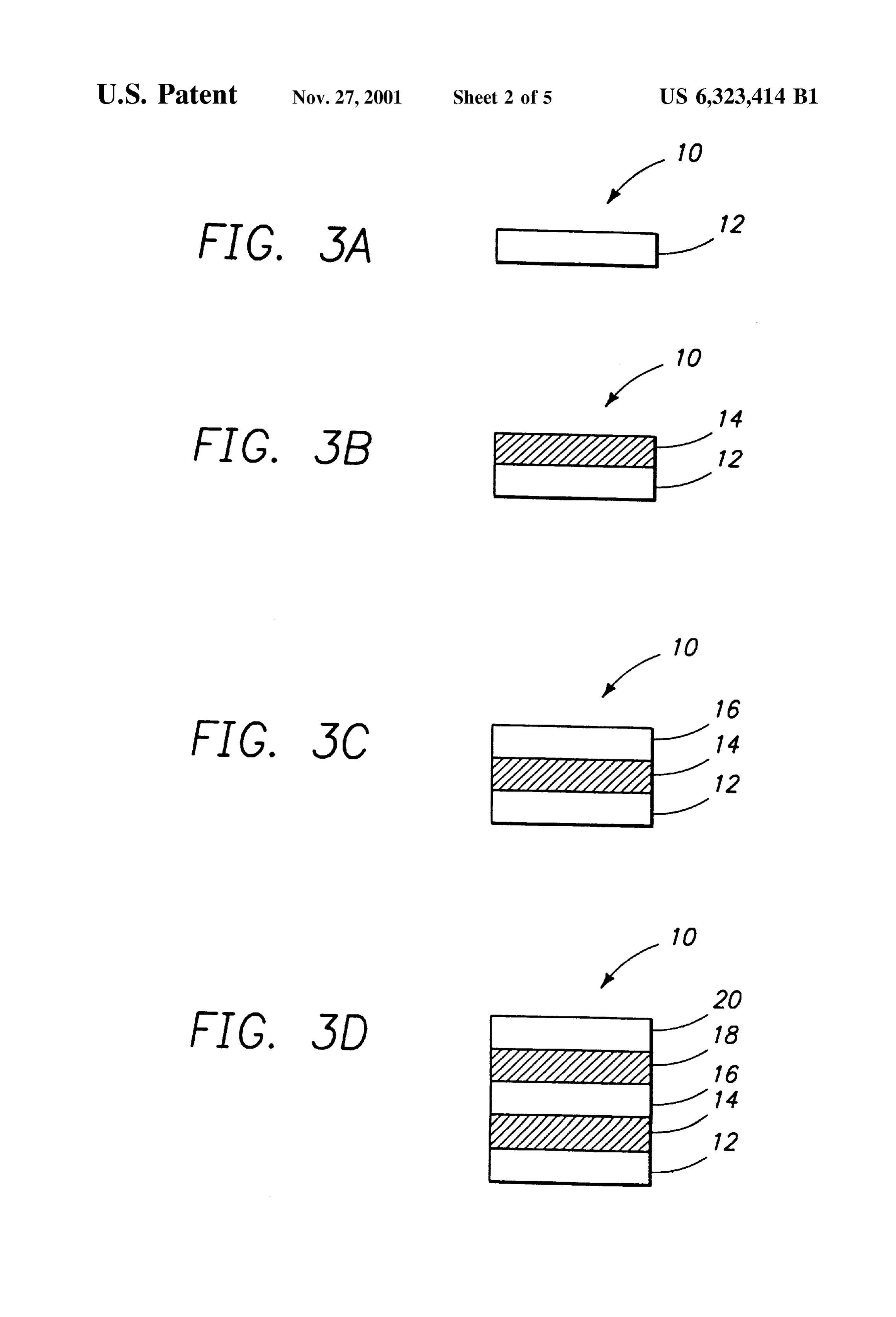
FIG. 3B shows device 10 being constructed by adding
layer 14 on top of layer 12. Layer 14 is a barrier layer for (p' should be high enough to SuppreSS the reverse current device 10, and for layer 12 consisting of GaAs, layer 14 is from anode to cathode. FIG. 1 shows the overall cooling typically a graded AlGaAS layer. Layer 14 creates a power for thermionic devices and thermoelectric devices. A Slight internal electric field throughout the thickness of layer Superior performance for HTI over TE cooling for all 14 to eliminate the Space charge problem around the cath currents is evident. FIG. 2 shows the ratio of the thermionic ode, which, in this case, is layer 12. Layer 14 is typically cooling term (p(I)+2 kT/e).I over the Peltier cooling term grown by MBE or MOCVD techniques, but can be grown in (S.T).I as a function of current. other ways. If layer 14 is n-type, layer 14 has a conduction By using the thermionic effect, instead of the thermoelec bandedge that increases as a function of the distance from tric effect, two immediate advantages are evident. The TE the layer 12, e.g., the value of the conduction bandedge at a cooler materials are restricted to those materials that have 35 first distance from the layer 12 is more than the value of the high electrical conductivity and thermopower, and low ther conduction bandedge at a Second, greater distance from the mal conductivity. These materials then only produce cooling layer 12. The layer 14 conduction bandedge increases for or heating at the junction between two materials, with layerS 14 that are doped n-type, corresponding p-type doped different Seebeck coefficients. layerS 14 will have a Valence bandedge that is decreasing. Heterostructure thermionic cooling, on the other hand, 40 The cally conduction bandedge of the layer 14 can be monotoni increasing, Stepped, or piecewise linear, or any other does not have a requirement for high thermopower materi als. Bandedge discontinuities, also known as Schottky shape, So long as at Some point in the layer 14 the conduction barriers, between the anode and cathode will perform the bandedge has a level higher than the conduction bandedge of cooling or heating as needed. One has to find the barrier the layer 12. Layer 14 can also be a Strained layer, to material that has high electrical conductivity and low ther 45 increase the bandedge offset between layer 12 and layer 14. mal conductivity. The cooling and/or heating effect pro For layerS 12 that are SiGe layer 14 can be a Silicon duced by thermionic devices, depending on the direction of germanium (SiGe), layer where y>X. For layers 12 that the current through the device, will be called a non are InGaAs, P. layer 14 is typically In-Gala isothermal effect, as it is a change in temperature in either ASP-2, where X-X, or ya-Y. For layers 12 that are direction from a device that has no current flow. 50 PbTe, layer 14 is typically Pb-EuTe. For layer 12 that is The Second advantage is that thermionic structures are HgCdTe., layer 14 is typically Hg2CdTe., where leSS space-consuming than TE coolers. Although both ther X-X. For layer 12 that is HgCdSe, layer 14 is mionic and TE coolers typically use a Series connection HgCdSe, where X-X. Layer 14 can also be made of between cooler elements to achieve lower temperatures, other materials, Such as Silicon oxide, aluminum oxide, thermionic coolers can be fabricated in a vertical manner, 55 Vacuum, air, indium gallium arsenide antimonide, indium Such that each cooler is Stacked on top of the other, whereas, gallium aluminum nitride, bismuth telluride, bismuth for practical connectivity reasons, TE coolers need to be Selenide, boron nitride, Zinc telluride, Zinc Selenide, lead tin fabricated in a planar manner to achieve reasonably high telluride, aluminum antimonide, lead telluride, other insu Voltage and reasonably low currents. The planar TE coolers lators, other gases, or other gradations or modulations of can then be Stacked for increased cooling. 60 materials for a given layer 12. The structure of FIG. 3B is an HTI device. The HTI
DETAILED DRAWINGS
device 10 of FIG. 3B can be used as a thermal imaging
FIGS. 3A-3E are diagrams of a first embodiment of the System, wherein the device 10 is a single pixel or multiple present invention. pixels of a thermal imaging System. FIG. 3A shows device 10 consisting initially of layer 12. 65 FIG. 3C shows device 10 in another format, where anode Layer 12 is typically gallium arsenide (GaAs), but can be layer 16 is added to device 10 on top of layer 14. Anode other materials, Such as Silicon (Si), indium phosphide (InP), layer 16 is typically made of the same material as layer 12,
Page 11
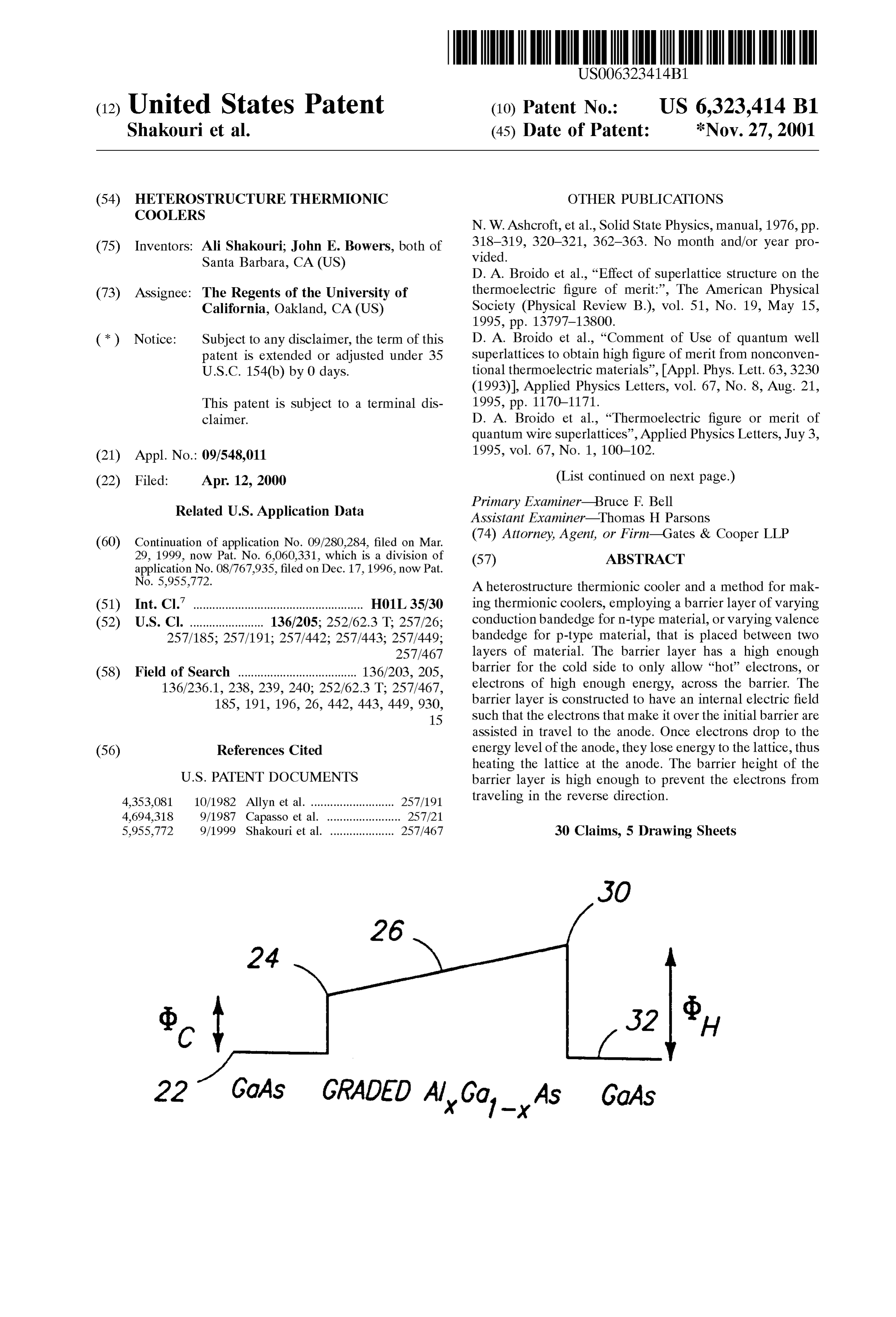
but can be made of other materials. Because of the gradation "hot electrons' because they are of Sufficient energy to carry or modulation of layer 14, the difference in conduction heat away from the cold junction at transition 24. bandedge between layer 16 and layer 14 is larger than the There will also be electrons in layer 12 that do not have difference in conduction bandedge between layer 12 and enough energy to get Over the barrier at transition 24. These layer 14. This difference in conduction bandedge between electrons are called “cold electrons' because they are not of the three layerS 12-16 creates, under an applied Voltage, a Sufficient energy to carry heat away from the cold junction. large forward current from layer 12 to layer 16 and a small AS the hot electrons get Over transition 24, the hot reverse current from layer 16 to layer 12. Within layer 14, electrons encounter the conduction bandedge of layer 14. the gradation or modulation creates a Small electric field that Under bias voltage V 34, the level 26 of the conduction assists electron movement away from layer 12 and through bandedge of layer 14 becomes tilted in the other direction, layer 14. e.g., it is slightly "downhill,” and thus aids the hot electrons FIG. 3D shows a series of layers 14-20 on layer 12 to in their travel away from the layer 12 and through the layer form device 10. This series connection creates two devices 14.
10 back to back, and thus, multiple forward and reverse Once the hot electrons get to transition 30, the hot barriers are created in Series. This Series connection places 15 electrons See a large energy drop because of the large the layers 14-20 in thermal series, which allows a larger difference in conduction bandege between layer 14 and layer temperature difference between the layer 12 and the final 16. The electrons lose their energy to the lattice, heating the layer 20 of the device 10. Layers 14-20 can be successive barrier layers, alternating barrier layerS and Semiconductor lattice layer up, and heating up the junction between layer 14 and 16, the hot junction of the device 10.
layers, or any combination of barrier layers and Semicon ductor layers. In the device 10, reversing the direction of the current will make a heterostructure thermionic heater. Note that the same
FIG. 3E is a diagram showing the selective removal of layer 14 in the device 10. After growing layer 16 on layer 14, device 10, in contact with two heat baths (a hot bath in certain portions 14 A of layer 14 can be removed by 25 12) willwith contact layer 16 and a cold bath in contact with layer produce electricity. This thermionic generator photolithography and dry or wet Selective etching tech should operate at temperatures much lower than required in niques. This creates a vacuum Space in layer 14, and Vacuum thermionic diode generators.
provides even lower thermal conductivity between layer 12 and layer 16. This structure allows for a precise cathode under FIG. 4C is a graph of several devices 10 placed in series anode Separation in an extremely Small space, namely the shown bias conditions. The device 10 has a structure as in FIG. 3D.
thickness of layer 14. Device 10 is a monolithic version of the original metal vacuum diodes. Layer 12 could be a The barrier layer can be graded So do is Small or Zero, as negative electron affinity material Such as aluminum nitride shown in FIG. 4D. These barrier layers can also be stacked (AIN), or coated with an electronegative material Such as as shown in FIG. 4E. The barrier layer does not have to be cesium. linear; FIG. 42 shows that the barrier layers can have a
FIGS. 4A-4E are graphs of the conduction bandedge of curved bandedge. The bandedge of the barrier layer can take an n-type device 10, or the Valence bandedge of a p-type any shape.
device 10 made using the present invention. For a p-type By operating the devices 10 in a cascade arrangement, device 10, the increasing energy is in the downward direc which is a Series thermal arrangement, higher temperature tion. 40 differences can be achieved. The first Stage of the cascade
FIG. 4A is a graph of the conduction bandedge of the (layers 36,38, and 40) provides a low temperature heat sink device 10. Level 22 is the conduction bandedge of layer 12. for the second stage (layers 40, 42, and 44) which in turn Transition 24 is the change in conduction bandedge at the provides a temperature Sink at an even lower temperature for boundary between layer 12 and layer 14. This amount, the third stage (layers 44, 46, and 48). By adding more labeled d, is the difference in conduction bandedge at the 45 Stages, more temperature heat SinkScan be added, and larger cold side of the device 10. Level 26 is the conduction temperature differences can be achieved. It is necessary that bandedge acroSS layer 14. This layer is increasing as the the cooling capacity of the higher temperature stages (layers distance from boudary 24 increases. Distance 28 is the 36,38, and 40) be greater than those which operate at lower thickness of layer 14. Distance 28 (see FIG. 4B) is typically temperatures (layers 40, 42, and 44 and layers 44, 46, and 0.01 to 1 micron. 50
Transition 30 is the change in conduction bandedge at the For example, the first stage (layer 36, 38, and 40) should boundary between layer 14 and layer 16. This difference, have a cooling power equal to the Sum of the cooling labeled d, is the difference in conduction bandedge at the capacities of all of the other Stages in the device, in this case, hot side of device 10. If level 26 increases across the the Second Stage (layers 40, 42, and 44), and the third Stage distance of layer 14, the transition 30 will have a larger 55 (layers 44, 46, and 48). This can be achieved by constructing difference than transition 24. Level 32 is the conduction the layers in a pyramid structure, shown in FIG. 5. bandedge acroSS layer 16. d can be Small, or even Zero, if The structure of FIG. 5 can be fabricated by using the maximum bandedge is at the beginning of layer 14, as Selective wet etching, or reactive ion etching, or other shown in FIG. 4D. techniques. Current flows through device 10 by having FIG. 4B shows the conduction bandedge graph of FIG. 4A electrons injected at contact 50 and emerging from contact
when device 10 is being biased. A bias voltage 34 is applied 52.
acroSS device 10, with the positive Voltage applied at layer The current can be adjusted within each Stage by injecting 16 and the negative voltage applied at layer 12. The level 22 current into or withdrawing current from contacts 54 and 56 of the conduction bandedge of layer 12 will thus be on the Side of the pyramid.
increased by bias voltage 34. Certain electrons in layer 12 65 The Series connection places the devices 10 in the Stack in will have enough energy to be able to get Over transition 24 thermal Series, which is easily done during the construction and continue on through layer 14. These electrons are called of the device 10.
Page 12
The same device 10 can be p-doped, resulting in a device are possible in light of the above teaching. It is intended that 10 that utilizes hole thermionic emission to perform the the scope of the invention be limited not with this detailed cooling task. The p-doped device 10 uses the bandedge description, but rather by the claims appended hereto. discontinuity in the Valence band to modify non-isothermal What is claimed is:
current transport in the device 10, Similar to the conduction 1. A thermionic device, comprising: band discontinuity in the n-doped electron thermionic device a first Semiconductor layer;
10 previously described. a first barrier layer, coupled to the first Semiconductor Devices 10 that are optimized for electron current cooling layer, wherein the first barrier layer selectively allows are not necessarily optimized for hole current cooling. Thus, an electronic charge carrier to Surmount a bandedge of materials that have larger Valence bandedge discontinuities the first barrier layer via thermionic emission; and and different effective masses may provide better cooling a heat Sink, coupled to the first barrier layer, wherein the performance under hole thermionic cooling than electron charge carrier that Surmounted the bandedge of the first thermionic cooling. barrier layer carries heat to the heat Sink. FIG. 4D shows the bandedge of a device 10 with a barrier 2. The thermionic device of claim 1, further comprising a layer as the final layer of the device 10. The layer 58 is the 15 Second Semiconductor layer attached between the first bar initial layer, and under bias voltage 60, the barrier layer rier layer and the heat Sink.
bandedge 62 will extend all the way down to level 64, which 3. The thermionic device of claim 2, further comprising at is at one end of the voltage potential for the device 10. The least one additional barrier layer attached between the bandedge 62 can take any shape. Second Semiconductor layer and the heat Sink. FIG. 4E shows the bandedge of a device 10 that has least 4. The thermionic device of claim3, further comprising at one additional Semiconductor layer attached between
Several devices 10 cascaded together. Layer 66 is coupled to the additional barrier layer 68. Barrier layer 68 is shown to have a curved barrier layer and the heat Sink. bandedge, but barrier layer 68 can have a bandedge of any least one additional device 5. The thermionic of claim 2, further comprising at shape. Barrier layer 68 is directly coupled to another barrier 25 Semiconductor layerS attachedalternating pair of between barrier layers and the Second Semicon layer 70, again shown with a curved bandedge. This cascade ductor layer and the heat Sink.
connection continues, with barrier layer 70 coupled directly 6. The thermionic device of claim 2, wherein the second to barrier layer 72, which is further coupled to barrier layer Semiconductor 74, ending at layer 76. layer 76 is coupled to the bias voltage conductor layer.layer is the same material as the first Semi
7. The thermionic device of claim 1, further comprising at
FIG. 6 shows a cascaded device using Stages with differ least one additional barrier layer attached between the first ent bandedge discontinuities. The difference in bandedge barrier layer and the heat Sink.
from level 80 to level 82 is not the same as the difference in 8. The thermionic device of claim 1, wherein a thickness bandedge between level 84 and level 86. The difference in of the first barrier layer is between 0.01 and 1 micron. bandedge from level 84 to level 86 is not the same as the 35 9. The thermionic device of claim 1, wherein the first difference in bandedge between level 88 and level 90. The Semiconductor layer is Selected from a group consisting of difference in bandedge from level 88 to level 90 is not the gallium arsenide, indium phosphide, Silicon, Silicon same as the difference in bandedge between level 92 and germanium, lead telluride, indium gallium arsenide level 94. Thus, the cascade Structure can accommodate (InGaAs), indium arsenide (InAs), indium antimonide different cooling capacities. 40 (InSb), indium gallium arsenide antimonide (In Ga FIG. 7 shows a combination of n-doped and p-doped xASSb), mercury cadmium telluride (HgCdTe), mer devices as described in the present invention. The combi cury cadmium Selenide (HgCdSe), gallium nitride nation of n-doped and p-doped devices 10 can be used in (GaN), aluminum gallium nitride (AlGaN), indium gal electrical Series, Similar to conventional thermoelectric cool lium nitride (In GaN), indium arsenide phosphide ers. The cascade structure of FIG. 7 will increase the cooling 45 (InASP), indium gallium arsenide phosphide (In Gai area of the device 10 without increasing the input current xASP), indium gallium aluminum arsenide (InGaAll through the device 10. Electrons are injected at contact 50 x-ySb), lead tin telluride (PbSn-Te), aluminum arsenide and emitted from contact 52. Electrons travel through each (AlAS), aluminum antimonide (AISb), Zinc Selenide (ZnSe), layer and contacts 56 in a Serpentine fashion, as in thermo Zinc telluride (ZnTe), boron nitride (BN), germanium (Ge), electric coolers. 50 gallium phosphide (Gap), gallium antimonide (GaSb), gal General Considerations lium aluminum arsenide (GaAl-AS), gallium arsenide The use of thermionic coolers provides a method for phosphide (GaAS, P), gallium indium phosphide (Gain cooling electronics that is currently unavailable. The use of aP), gallium indium antimonide (GanSb), bismuth tel both electron and hole thermionic emission to cool electron luride (Bi-Te), and bismuth Selenide (Bi-Sea), where the ics will allow for Small thermionic coolers that can be 55 Subscripts X, y, 1-X, and 1-y denote the relative amounts of fabricated as part of integrated circuits to allow those the atomic species in each ternary or quartenary materials circuits to be cooled while in use in various applications. and range from Zero to one, inclusive. In the description of the preferred embodiment, reference 10. The thermionic device of claim 1, wherein the first is made to the accompanying drawings which form a part barrier layer is Selected from a group consisting of alumi hereof, and in which is shown by way of illustration the 60 num gallium arsenide, indium gallium arsenide phosphide, Specific embodiment in which the invention may be prac Silicon germanium, lead europium telluride, Silicon oxide, ticed. It is to be understood that other embodiments may be aluminum oxide, Vacuum, mercury cadmium telluride, mer utilized as Structural changes may be made without depart cury cadmium Selenide, indium gallium arsenide ing from the Scope of the present invention. antimonide, indium gallium aluminum nitride, bismuth The description of the preferred embodiment is not 65 telluride, bismuth Selenide, boron nitride, Zinc telluride, Zinc intended to be exhaustive or to limit the invention to the Selenide, lead tin telluride, aluminum antimonide, lead precise form disclosed. Many modifications and variations telluride, and air.
Page 13
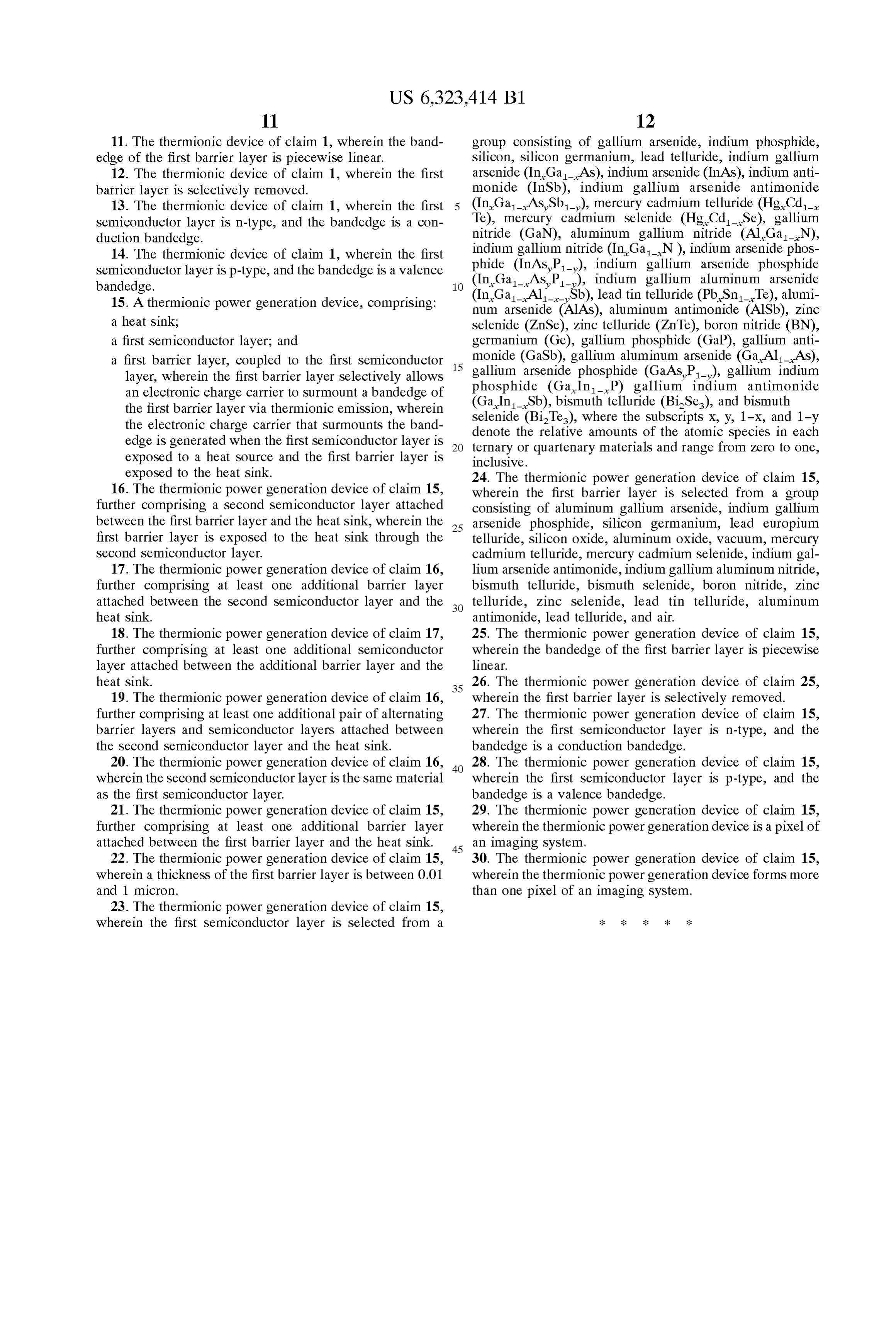
11. The thermionic device of claim 1, wherein the band group consisting of gallium arsenide, indium phosphide, edge of the first barrier layer is piecewise linear. Silicon, Silicon germanium, lead telluride, indium gallium 12. The thermionic device of claim 1, wherein the first arsenide (InGaAs), indium arsenide (InAs), indium anti barrier layer is Selectively removed. monide (InSb), indium gallium arsenide antimonide 13. The thermionic device of claim 1, wherein the first (InGaAS,Sb), mercury cadmium telluride (HgCd1 Semiconductor layer is n-type, and the bandedge is a con Te), mercury cadmium Selenide (HgCdSe), gallium duction bandedge. nitride (GaN), aluminum gallium nitride (AlGaN), 14. The thermionic device of claim 1, wherein the first indium gallium nitride (In GaN), indium arsenide phos Semiconductor layer is p-type, and the bandedge is a Valence phide (InAS,P,-), indium gallium arsenide phosphide bandedge. (InGaAsP,-), indium gallium aluminum arsenide 15. A thermionic power generation device, comprising: (InGaAll-Sb), lead tin telluride (PbSni-Te), alumi num arsenide (AIAS), aluminum antimonide (AlSb), Zinc a heat Sink, selenide (ZnSe), zinc telluride (ZnTe), boron nitride (BN), a first Semiconductor layer; and germanium (Ge), gallium phosphide (GaP), gallium anti a first barrier layer, coupled to the first Semiconductor 15 monide (GaSb), gallium aluminum arsenide (GaAl-AS), layer, wherein the first barrier layer selectively allows gallium arsenide phosphide (GaAS, P), gallium indium an electronic charge carrier to Surmount a bandedge of phosphide (Gan-P) gallium indium antimonide the first barrier layer via thermionic emission, wherein (GanSb),
Selenide bismuth telluride (BiSea), and bismuth
(Bi-Te), where the Subscripts x, y, 1-X, and 1-y the electronic charge carrier that Surmounts the band edge is generated when the first Semiconductor layer is denote the relative amounts of the atomic species in each ternary or quartenary materials and range from Zero to one, exposed to a heat Source and the first barrier layer is inclusive.
exposed to the heat Sink. 24. The thermionic power generation device of claim 15, 16. The thermionic power generation device of claim 15, wherein the first barrier layer is Selected from a group further comprising a Second Semiconductor layer attached consisting of aluminum gallium arsenide, indium gallium between the first barrier layer and the heat sink, wherein the 25 arsenide phosphide, Silicon germanium, lead europium first barrier layer is exposed to the heat Sink through the telluride, Silicon oxide, aluminum oxide, Vacuum, mercury Second Semiconductor layer. cadmium telluride, mercury cadmium Selenide, indium gal 17. The thermionic power generation device of claim 16, lium arsenide antimonide, indium gallium aluminum nitride, further comprising at least one additional barrier layer bismuth telluride, bismuth Selenide, boron nitride, zinc attached between the Second Semiconductor layer and the telluride, Zinc Selenide, lead tin telluride, aluminum heat Sink. antimonide, lead telluride, and air. 18. The thermionic power generation device of claim 17, 25. The thermionic power generation device of claim 15, further comprising at least one additional Semiconductor wherein the bandedge of the first barrier layer is piecewise layer attached between the additional barrier layer and the linear.
heat Sink. 26. The thermionic power generation device of claim 25,
19. The thermionic power generation device of claim 16, wherein the first barrier layer is selectively removed. further comprising at least one additional pair of alternating 27. The thermionic power generation device of claim 15, barrier layers and Semiconductor layerS attached between wherein the first Semiconductor layer is n-type, and the the Second Semiconductor layer and the heat Sink. bandedge is a conduction bandedge. 20. The thermionic power generation device of claim 16, 40 28. The thermionic power generation device of claim 15, wherein the Second Semiconductor layer is the same material wherein the first Semiconductor layer is p-type, and the as the first Semiconductor layer. bandedge is a Valence bandedge. 21. The thermionic power generation device of claim 15, 29. The thermionic power generation device of claim 15, further comprising at least one additional barrier layer wherein the thermionic power generation device is a pixel of attached between the first barrier layer and the heat sink. 45 an imaging System.
22. The thermionic power generation device of claim 15, 30. The thermionic power generation device of claim 15, wherein a thickness of the first barrier layer is between 0.01 wherein the thermionic power generation device forms more and 1 micron. than one pixel of an imaging System. 23. The thermionic power generation device of claim 15, wherein the first Semiconductor layer is Selected from a k k k k k
Page 14
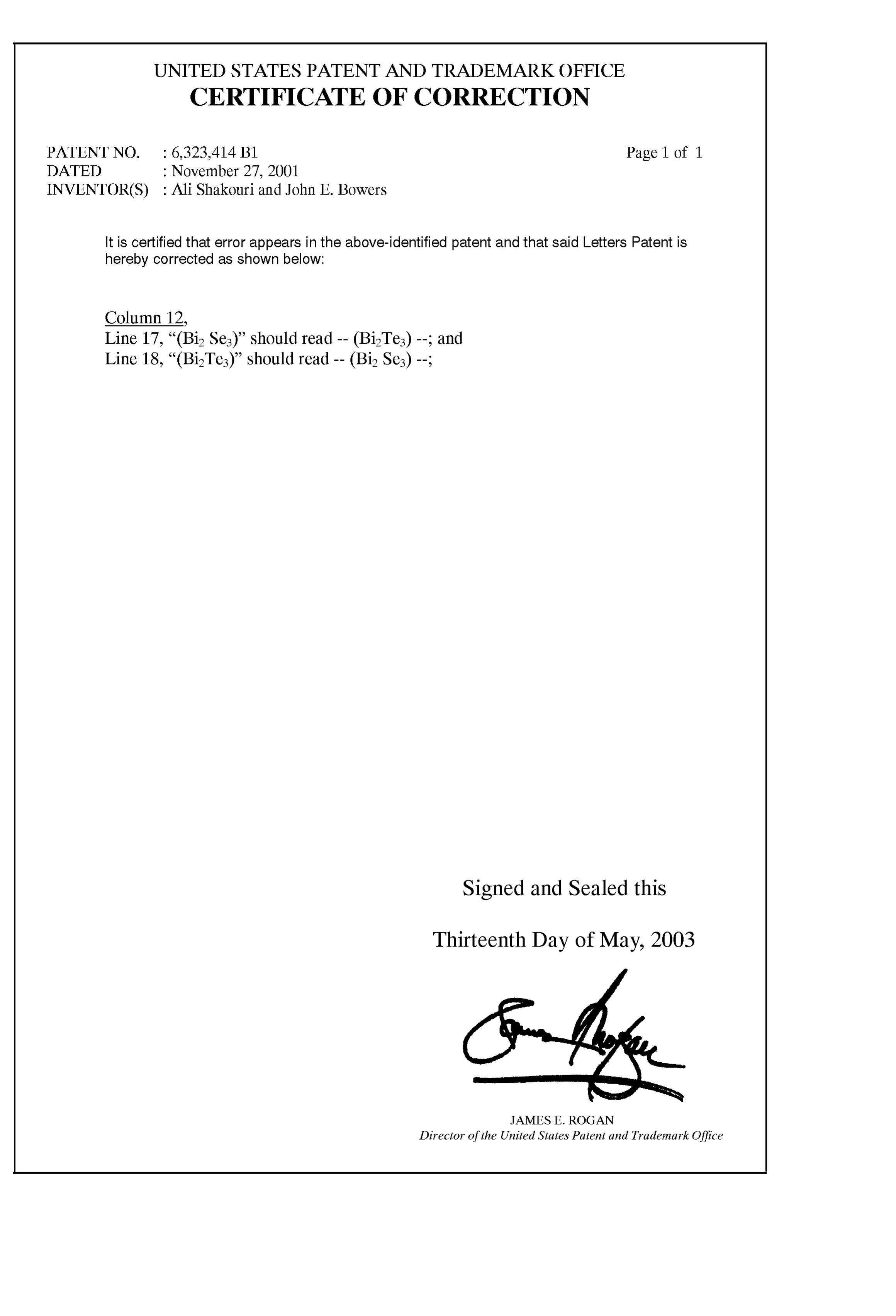
UNITED STATES PATENT AND TRADEMARK OFFICE
CERTIFICATE OF CORRECTION
PATENT NO. : 6,323,414 B1 Page 1 of 1
INVENTOR(S) : Ali Shakouri and John E. Bowers It is certified that error appears in the above-identified patent and that said Letters Patent is hereby corrected as shown below:
Column 12,
Line 17, "(Bi Ses) should read -- (BiTes) --; and Line 18, "(BiTes)” should read -- (Bi Ses) --; Signed and Sealed this
Thirteenth Day of May, 2003
JAMES E ROGAN
Director of the United States Patent and Trademark Office
Provenance
- Collection
- Cited prior art
- Original PDF
- patentimages.storage.googleapis.com →
- Filed
- 2000-04-12
- Pages
- 14
- Method
- pdftotext (the PDF's own text layer) + pdftoppm 300dpi page scans
- Source
- Google Patents bibliographic record
- Granted
- 2001-11-27
- Inventors
- Ali Shakouri; John E. Bowers; University of California San Diego UCSD
- Transcribed from
- patentimages.storage.googleapis.com →