patent · US6133989
3D imaging laser radar
17 October 2000
Page 1 — bibliographic record
United States Patent (19) 11 Patent Number: 6,133,989 Stettner et al. (45) Date of Patent: *Oct. 17, 2000 54) 3D IMAGING LASER RADAR 57 ABSTRACT 75 Inventors: Roger Stettner; Howard W. Bailey, A three dimensional imaging device is presented which uses both of Santa Barbara, Calif. Single pulse from a pulsed light Source for detecting objects 73 Assignee: Advanced Scientific Concepts, Inc., enveloped by a light-transmitting medium Such as the Santa Barbara, Calif. earth's atmosphere or free Space. By means of Switching off a ramping Voltage, individually for each object pixel, the * Notice: This patent is Subject to a terminal dis time of arrival of the reflected pulse is recorded. This time claimer. is related to the third object dimension. The device consists of the pulsed light Source, optics for collecting the reflected 21 Appl. No.: 08/665,738 light, a Sensor for detecting the light, drive and output 22 Filed: Jun. 19, 1996 electronics for timing and Signal conditioning of data gen erated by the Sensors and a computer for processing the
Related U.S. Application Data Sensor data and converting it to a three dimensional image. The Sensor collects and processes the light data in a unique 63 Continuation-in-part of application No. 08/015,627, Feb. 9, manner, using a hybrid. The hybrid is actually a two dimen 1993, Pat. No. 5,446,529. Sional array of collectors or detectors combined in very close (51) Int. Cl. ............................................... GO1C 03/08 proximity with their own processing electronics. In general, 52 U.S. C. ... ... 356/401; 250/332 the hybrid is composed of two integrated circuit chips mated 58 Field of Search .................................. 356/5.03, 5.04, together. The two dimensional array defines two dimensions 356/4.01; 250/332, 339.02 of the image. The processing electronics individually and 56) References Cited independently Switch off, at high-Speed, a time varying Voltage when the light pulse, reflected from the object,
5,220,164 6/1993 Lieber et al. ..................... 250/214 VT mathematically transformed to the third object dimension. 5,243,541 9/1993 Ulich ....................................... 364/516 The Sensor also records peak light pulse information which 5,446,529 8/1995 Stettner et al. ........................ 356/4.01 can be used to obtain higher resolution in the third dimen
Primary Examiner Mark Hellner
Attorney, Agent, or Firm-Gottlieb, Rackman & Reisman,
P.C. 75 Claims, 5 Drawing Sheets
Page 2
Drawing sheet — no readable text.
Page 3
Drawing sheet — no readable text.
Page 4
Drawing sheet — no readable text.
Page 5
Drawing sheet — no readable text.
Page 6
Drawing sheet — no readable text.
Page 7
3D IMAGING LASER RADAR BRIEF DESCRIPTION OF THE PRESENT
INVENTION
This application is a continuation-in-part of application
Ser. No. 08/015,627 filled Feb. 9, 1993, 3D Imaging Under The present invention overcomes the limitation of mul water Laser Radar (herein called Reference 1), now U.S. tiple laser radar receivers for Single-pulse imaging by Pat. No. 5,446,529. employing a hybrid chip design and unique integrated
BACKGROUND OF THE INVENTION
circuitry. The hybrid is typically composed of two chips, an array of detectors (or collectors) directly connected to an
This invention relates to a laser radar Vision apparatus array of processing-electronics unit cells. Each detector/ capable of producing a three-dimensional image of a distant 1O collector, on one chip, is connected to its own processing target. electronicS unit cell, on the other chip, and defines a pixel in In particular, it relates to a lightweight, multiplexing, the image. Each processing-electronicS unit cell, on the electronic apparatus for capturing a three-dimensional (3D) array, contains an identical and unique integrated circuit image of a distant target at high-Spatial and high-range which can Store the reflected-pulse transit time for a target resolution in the atmosphere or in Space with a single laser pixel as well as Store amplitude information required for pulse. 15 high-range resolution. The transit-time information for all
Laser radars (ladars) determine range in the atmosphere pixels is multiplexed off the hybrid between laser pulses. by measuring the transit time of a laser pulse from the Each detector/collector with its processing-electronics unit transmitter/receiver to the target and dividing by twice the
Velocity of light in the atmospheric medium. Range resolu cell is equivalent to an independent laser radar receiver. tion in Such devices is related to the accuracy of this transit directly with thearedetector
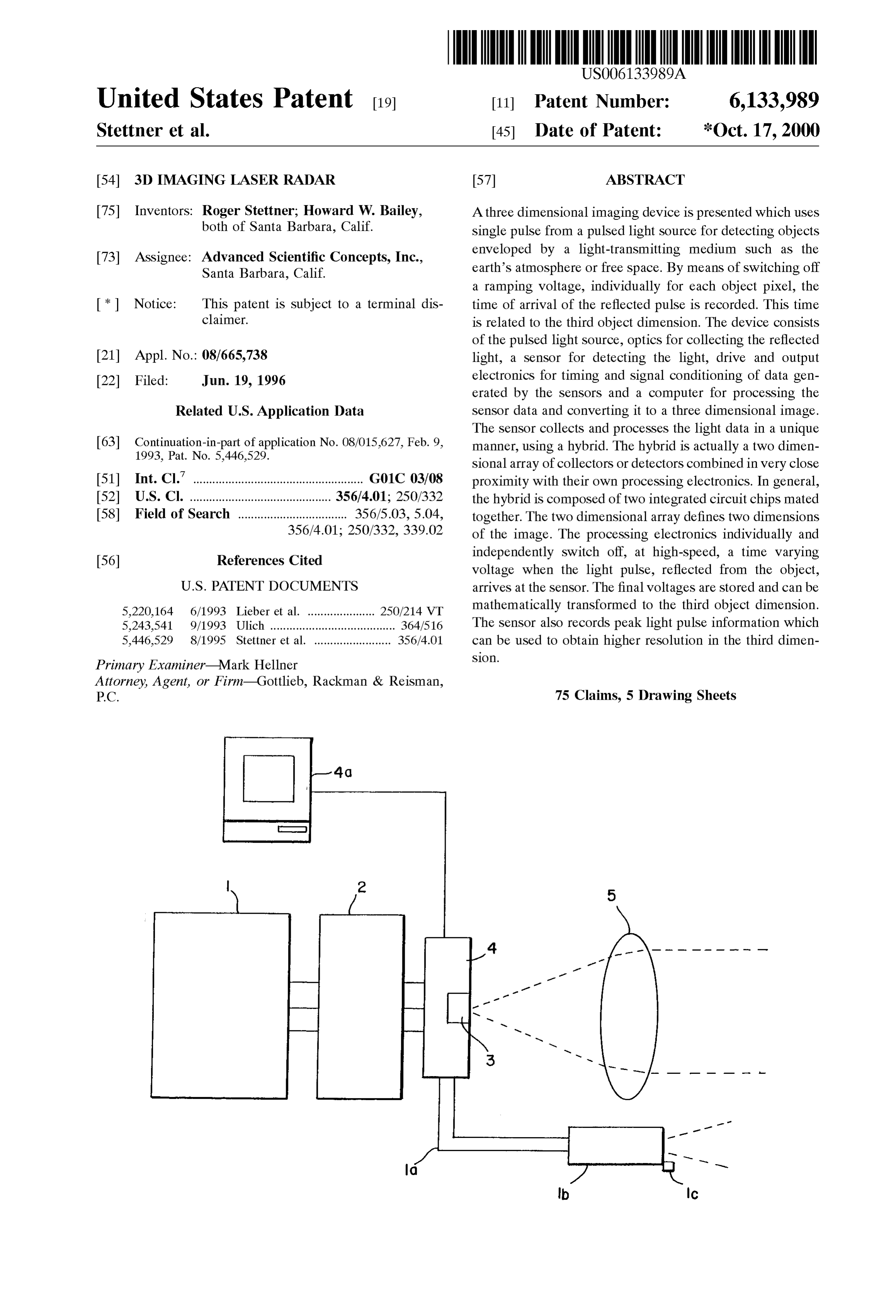
Embodiments presented where laser photons interact array generating a Signal or where time measurement. In the atmosphere, ranges are typically the laser measured in kilometers, where range resolution can be as generate the Signal. photons are converted to electrons which then Small as 30 cm. A 3D target image can be obtained with a laser radar by rastering the laser beam acroSS the target and It is the object of the present invention to provide a device measuring the transit time, pulse by pulse, where each pulse 25 for three dimensional imaging of objects by transit time corresponds to a point on the target. The distance between measurements in transparent media and to overcome the points on the target determines the Spatial resolution of the problems of prior Systems associated with the need for rastered image and defines the picture element (pixel) Size; Storing Signals from multiple range resolution intervals, for the number of pixels at the target determines the pixel-array mechanical Scanning and for multi-pulse target coverage. size; the range resolution determines resolution in the third The device comprises a pulsed light Source, means for target dimension. Rastering is a Slow process, particularly projecting the light towards the object, optics for collecting for large pixel-array sizes, and it requires cumberSome the reflected light, improved Sensors for detecting the mechanical Scanners and complex pixel-registration com reflected light, drive and output electronics for timing and puter processing. Signal conditioning of data from the Sensors and a computer When high-Speed imaging is required, it is desirable to 35 and Software for converting the Sensor data to a three obtain the entire image with one laser pulse. However, dimensional image.
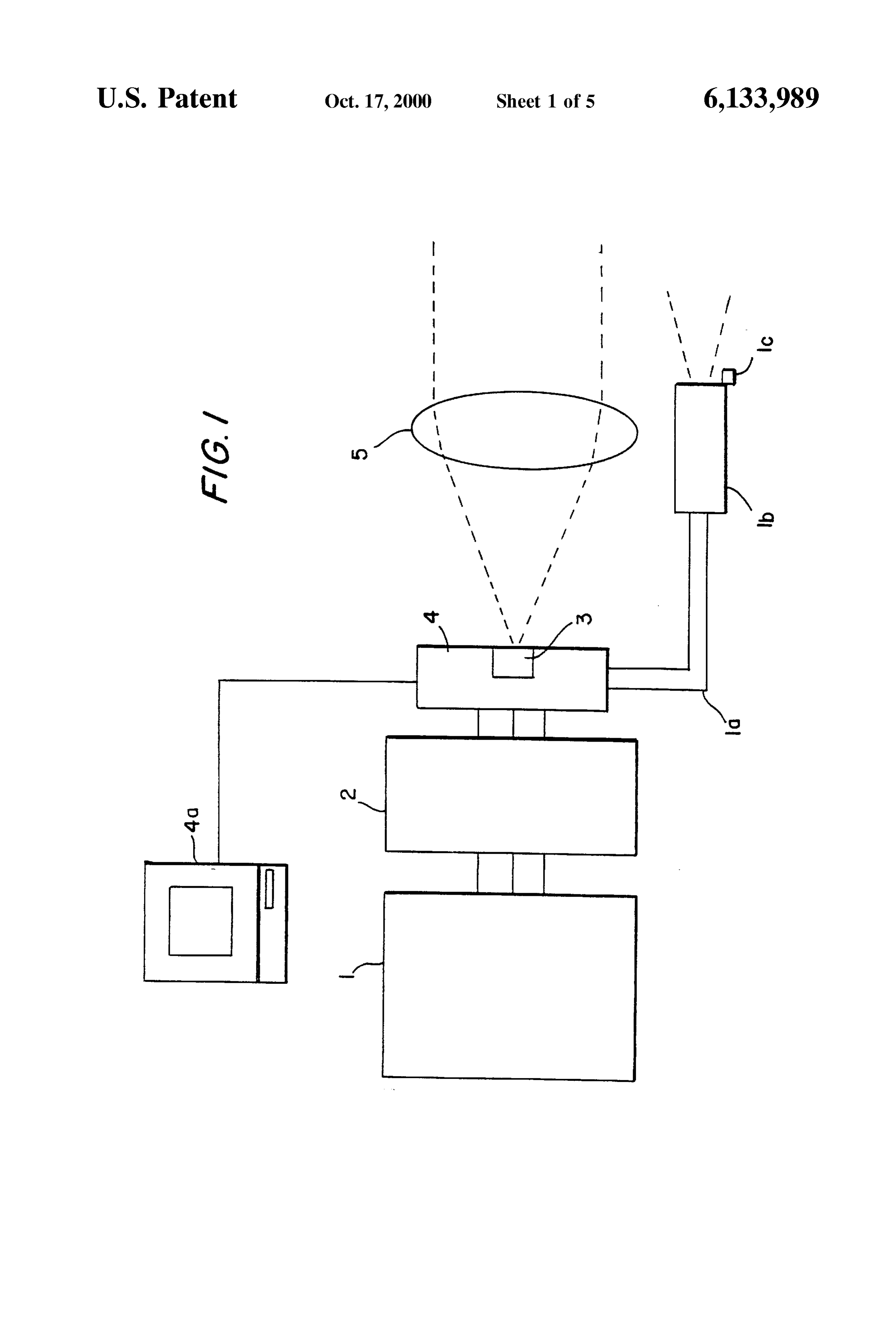
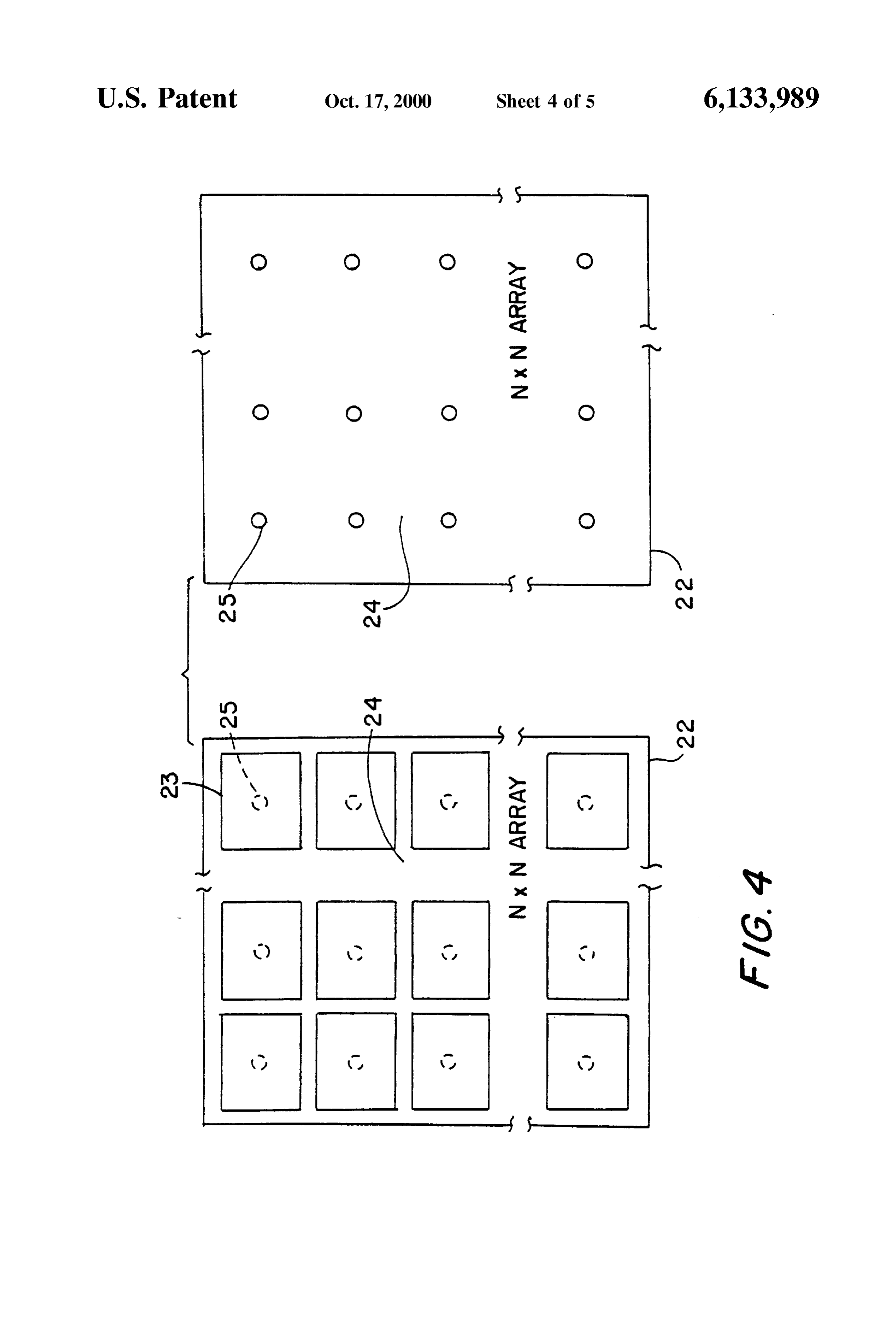
because of weight, cost and complexity problems, it is It is further the object of the present invention to provide undesirable to obtain the entire image with independent, Sensors which detect and Store target-reflected laser-light parallel, laser radar receivers, where each pixel uses a transit-time and peak amplitude information on a Separate laser radar receiver System; multiplexing with one 40 processing-electronics unit cell array from which the range laser radar receiver should be used to make a large pixel of each target pixel can be accurately determined. array imaging System practical. Currently there are no lightweight, Small-size, multiplexing laser radar receivers BRIEF DESCRIPTION OF THE DRAWINGS which can image an entire target, in the atmosphere, with a FIG. 1 is a side view of the preferred embodiment of the Single laser pulse at large pixel-array size and high-range 45 Laser Radar Focal Plane Array Imaging System. resolution. Reference 1, however, discloses a lightweight, FIG. 2 is a perspective view of the hybrid sensor of the multiplexing laser radar receiver which can image an entire present invention.
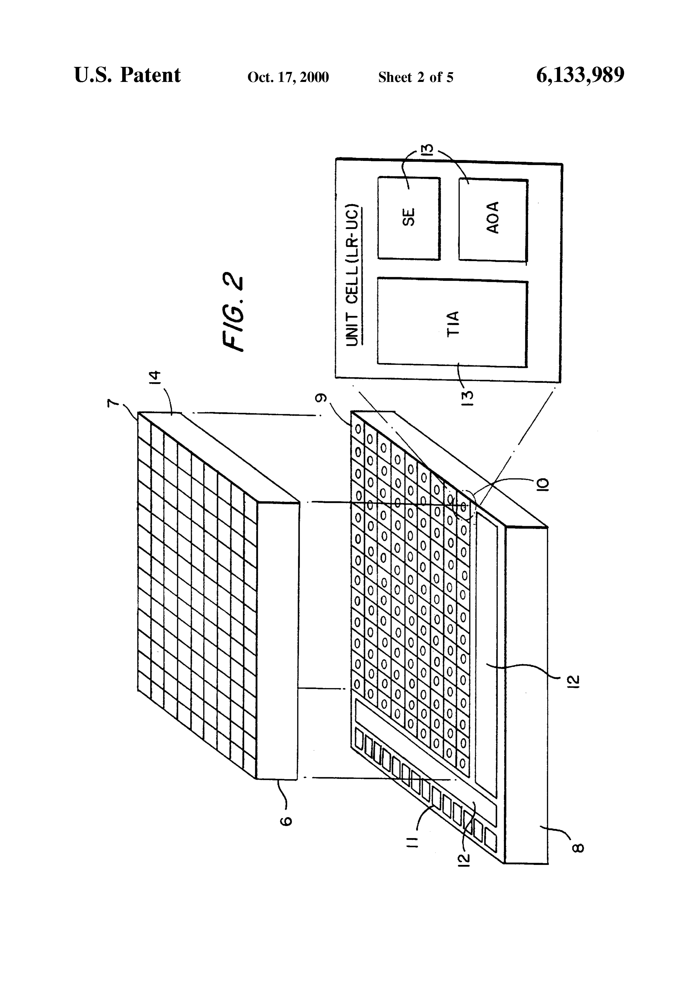
target, in water, with a single laser pulse. It accomplishes FIG. 3 is a side view of the vacuum tube sensor of the this feat by Storing the reflected Signal from each range resolution interval to determine, by means of a signal 50 present invention.
amplitude comparison, the time of laser pulse returned. FIG. 4 is a top and side view of the anode array of the Because the range of lasers in the atmosphere is 10 to 100 present invention.
times the range in water, but the range resolutions are FIG. 5 is a block diagram of the unit cell processing comparable, it is impractical to Store the Signal from the electronics of the present invention.
too-numerous range resolution intervals and evaluate transit 55 DETAILED DESCRIPTION OF A PREFERRED time to a target. Instead the returning pulse must Stop a EMBODIMENT OF THE INVENTION clock. This clock can be a Voltage ramp; that is a voltage which is decreasing in time. The Voltage at which the ramp A preferred embodiment of the present invention, the is Switched off determines the time at which the laser pulse Laser Radar Focal Plane Array (LR-FPA) imaging system returned. The Voltage ramp begins when the laser pulse is 60 depicted in FIG. 1, is designed to produce three-dimensional transmitted. Because Stopping a clock or Switching off a image data (area and range) from a single laser pulse Voltage ramp is usually dependent upon the returning-pulse reflected from objects in the atmosphere, using transit time amplitude for typical laser pulse widths (due to the clock information, and process the data to form a three dimen Stopping circuitry) and the returning-pulse amplitude is Sional image. Six parts make up the preferred embodiment dependent, pixel by pixel, on the reflectivity of the target, the 65 of the invention; a pulsed laser 1, with delivery System 1a, range must be corrected for amplitude to obtain high range collimator 1 and laser transmission detector 1C the data resolution. processing and laser control System 2, the Sensor 3, and
Page 8
asSociated output and drive electronics 4, and the optics 5. The LR-FPA imaging system functions as follows. A The output and drive electronicS 4 is electrically connected pulsed laser 1 (FIG. 1) emits a laser pulse, via a delivery to an image processing computer 4a. System 1a and collimator 1b, towards a target. A laser FIG. 2 shows one Sensor design 3, a hybrid Sensor, in transmission detector 1c gates on the clock to Start the ramp greater detail. It consists of a detector array chip 6, com voltage ØTM (FIG. 5) located within the output and drive posed of individual detectorS 7, the laser radar processor electronicS 4. The collimator is designed So that the laser chip 8, and indium bumps 9, which electrically connect each pulse illuminates all or a large part of the target and not just detector 7 to a Single, corresponding, laser radar processor one point. Laser light reflected from the target is captured by unit cell 10. Wire bond pads 11 electrically connect the the optics 5 and focused on the sensor 3. Light absorbed by hybrid sensor 3 to the drive and output electronics 4. the detectors 7 (sensor in FIG. 2 only) of the detector array Multiplexing and output amplifier circuitry 12 connect the 6 are converted to electrons and holes and each is conducted unit cell circuitry 13 with the wire bond pads 11. In the by detector internal fields to opposite Sides of the detector hybrid sensor 3, laser light interacts directly with the detec substrate 14. Charges that conduct to the bottom of the tors which are Solid State devices that are responsive to the substrate 14 are conducted through the indium bump 9 as an particular laser wavelength. The detectors are made on a 15 electric currents to laser radar processor unit cells 10 cor solid-state substrate 14. The detector size can be 10 um to responding to the detectors 7 that absorbed the laser photons. 500 um on a side. The array size can be 4x4 to 1024x1024.
Typically the chips are a few centimeters Square. For intense reflected Signals or where the Size of the laser radar
For intense Sources the detector array chip 6 may be incorporate processor unit cell 10 is large, a monolithic design can combined with the laser radar processor chip 8 in a mono cessor unit cell a Small detector 7 into in the laser radar pro 10. Under these circumstances the detector lithic design. In this configuration a Small detector 7 would current flows directly into the unit cell processing electron be incorporated in the laser radar processor unit cell 10.
FIG.3 shows an alternate Sensor design, the vacuum tube ics much as depicted in FIG. 5. Sensor 3, where the detector array chip 6, is bump bonded to If the FIG. 3 vacuum tube sensor 3 is employed with the the laser radar processor chip 8, and enclosed in a vacuum 25 LR-FPA imaging system depicted in FIG. 1 as before, laser tube 15. The vacuum tube contains a fiber optic window 16 light reflected from the target is captured by the optics 5 and to channel the laser light to a photocathode 17, where the focused on the Sensor 3. Laser photons are channeled by the laser light is converted to photoelectrons. A Voltage between fiber optic window 16 to the photocathode 17 where the laser the photocathode and the detector array generates a large light is converted to photoelectrons. The photoelectrons are electric field, E, in the tube to accelerate the electrons into accelerated by the electric field, E, into the detector array 6, the detector array 6. The laser radar processor chip 8 is where the Signal is amplified. Amplification results because mounted on a ceramic chip carrier 18 which contains wire it requires about three times the bandgap of the detector Solid bond pads 19 that communicate with the drive and output State material, or typically about 3 eV, to create an electron electronics 4 (FIG. 1) and laser radar processor chip 8 by hole and pair and the potential drop between the photocathode the detector array is many keV. Although Some energy means of wires 20. The vacuum tube 15 may also contain 35 guard rings 21 at the same potential as the detector array. is lost in penetrating into the active area of the detectorS 7, Typically the FIG. 3 sensor is few centimeters in all three the energy that remains will create multiple electron-hole pairs for each photoelectron and hence amplification.
dimensions.
In the FIG. 3 sensor configuration the detector array 6 can Charges that conduct to the bottom of the substrate 14 are either be a Solid-State detector array or an anode array. An 40 conducted to laser through the indium bump 9 as an electric current radar processor unit cells 10 corresponding to the anode array 22 is depicted in FIG. 4. The anodes 23 are metal pads on top of a ceramic Substrate 24, that collect detectors 7 that absorbed the laser photons. electrons and pass the electrical Signal through metal Vias 25 If the FIG. 4 vacuum tube sensor 3 employs a detector in the ceramic substrate 24 to indium bumps 9 at the array 6 which is an anode array 22 the photoelectrons are underside of the anode array. Contact to the indium bump 9 45 collected by the anodes, without amplification, and are is made at the metal via 25 on the bottom of the Substrate 24. conducted as electric current through the Vias 25, through When the FIG.3 sensor is used with the FIG. 4 anode array, the indium bump 9 to laser radar processor unit cells IQ the Sensor a can also contain a microchannel plate between corresponding to the anodes 23 that absorbed the photoelec the photocathode 17 and the anode array 6 in an alternate trOnS.
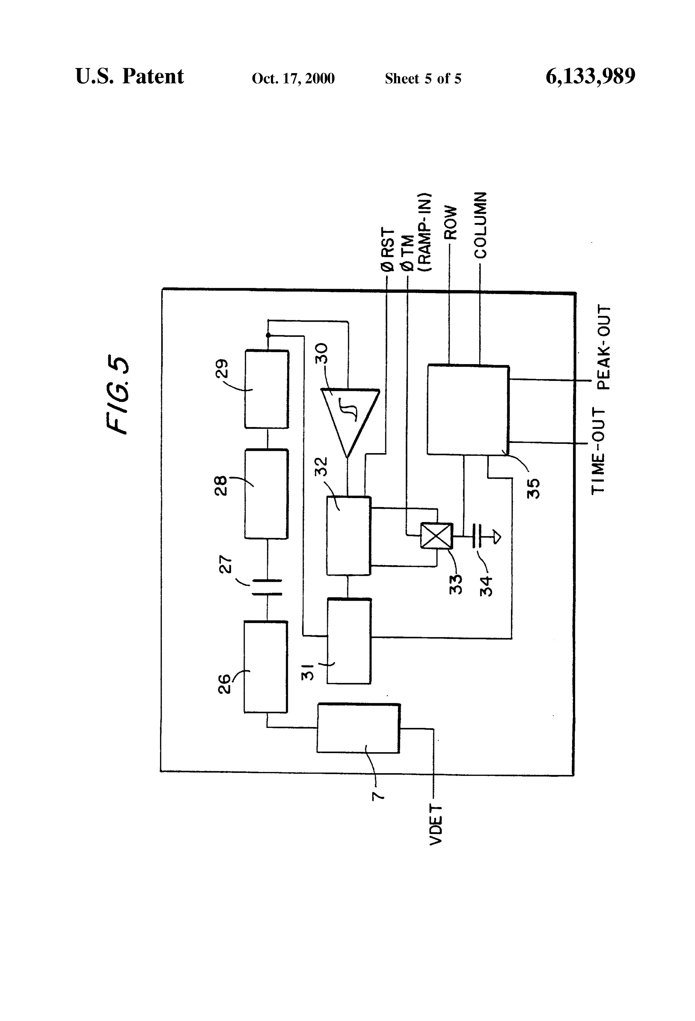
design; the microchannel plate is not shown in the figure. 50 The FIG. 4 vacuum tube sensor 3 employing a detector In an alternate Sensor 3 design, the FIG. 3 Sensor may be array 6 which is an anode array 22 can also be used, in an placed in a magnetic field oriented perpendicular to the alternate configuration, to amplify the photoelectrons: a photocathode 17. microchannel plate is placed between the photocathode 17 FIG. 5 shows a block diagram of the unit cell circuitry 13 and the anode array 22. In this case the electric field (FIG. 2). The detector 7 inputs a current signal to a tran 55 accelerates the electrons into the top of the microchannel Simpedance amplifier 26 which is AC coupled by means of plate tubules. A Voltage acroSS the microchannel plate causes coupling capacitor 27 to a high pass filter 28 and then to an multiplication of the photoelectrons in the microchannel amplifier 29. The amplified Voltage Signal is passed on to plate tubule. A voltage from the bottom of the microchannel both a Schmitt Trigger 30 and a peak detector 31. If the plate to the anode array 22 accelerates the electrons to the Signal is large enough, the transit-time memory 32 will 60 anode array 22 and these are collected by the anodes 23. The change State and open Switch 33. This terminates the charg electrons collected by the anodes 23 form a detector current ing of memory capacitor 34 by the ramp voltage ØTM. Both which is conducted through the vias 25, through the indium the peak detector 31 and the analog memory 34 are con bump 9 to laser radar processor unit cells 10 corresponding nected to the output amplifier circuitry 35. There may be a to the anodes 23 that absorbed the amplified electrons. plurality of memory capacitors 34 and the means to Switch 65 All the FIG. 4 vacuum tube sensors 3 can be used in a between them, corresponding to multiple reflections from magnetic field oriented perpendicular to the photocathode multiple objects. 17. The magnetic field increases the spatial resolution of the
Page 9
S 6 invention by preventing lateral translation of photoelectrons than one peak detector analog memory may be present in the emitted with Velocity components parallel to the photocath peak detector block 21. Correspondingly more than one ode. The electrons Spin around a magnetic field line in their transit-time memory 32 may also be present. The electrical transit to the detector array 6. means for Switching between these memories would also be The detector currents are processed by the laser radar present in the laser radar processor unit cell 10 designed for processor unit cell circuitry 13, for all sensors 3 as follows. multiple reflections. Typically the Switching would be per Detector currents are input to the oft transimpedance ampli formed by shift register in the processing electronics unit fier 26 and converted to a Voltage. Because of input cell circuitry 13.
capacitance, the transimpedance amplifier circuitry also acts After the maximum time required for laser pulse return, like a low pass filter only allowing input frequencies lower the drive electronics 4 begins Sequencing through the laser then or equalit to those of the laser pulse to pass through to radar processor unit cells 10, reading out the data. When the next processing Stage. The coupling capacitor 27 both the Row and Column lines of a particular unit cell are removes constant current Sources, Such as detector dark activated, the Output Amplifier circuitry 35 switches the current, from the Voltage Signal. The high pass filter 28 arrival-time voltage, TIME-OUT, and the peak-detector removes the lower frequency noise leaving only those 15 voltage PEAK-OUT, onto the output lines and they are frequencies associated with the laser pulse. The combination driven by the output amplifier to the output and multiplexing of low pass filtering, constant current filtering and high pass circuitry 12, FIG. 2, which drives the signals to the output filtering removes most of the Signal noise and improves the electronicS 4. The arrival-time Voltage and peak-detector Signal-to-noise ratio and consequently the Sensitivity of the Voltage are processed by the image processing computer 4a unit cell circuitry. The output of the high pass filter 28 is fed and displayed as a 3D image. After the drive and output into an amplifier 29 to increase the sensitivity of the unit cell electronics 4 has processed the laser radar processor unit cell circuitry to low-amplitude laser pulses. Output of the ampli 8 output voltages, each unit cell memory 32 is reset by a fier 29 is fed directly into a Schmitt Trigger 30. The function drive-electronics 4 generated pulse, making this unit cell of the Schmitt Trigger 30 is to reshape the incoming wave ready for the next laser pulse.
form into a Square wave, with fast rise and fall times, after What is claimed is:
a set trigger level is reached. The Schmitt Trigger 30 25 1. A device for imaging Sections of a three dimensional provides positive feedback for Saturation to occur rapidly objects immersed in a light conducting medium comprising: and therefore produce Sharp rise times. a pulsed light Source;
The state of the transit-time memory 32 will either means for transmitting light from Said pulsed light Source connect or disconnect the Switch 33 from the external ramp into Said medium;
voltage (OTM. Just prior to the emission of the laser pulse, optics for collecting light from Said medium during the the transit-time memory 32 is reset so the Switch 33 is closed time for light to transit from Said pulsed light Source, and the ramp Voltage can be fed directly into the analog reflect from Said objects and be collected by Said optics, memory 34. The analog memory 34 is typically a capacitor a Sensor means for detecting Said collected light, Said that is charged by the ramp Voltage. A laser pulse changes Sensor means comprising the memory State of the transit-time memory 32, via the 35 means for converting Said collected light into electrical Schmitt Trigger, and opens the Switch 33 preventing further charge, charging of the analog memory 34 by the ramp Voltage. The a hybrid comprising final Voltage on the analog memory 34 is directly related to the laser pulse transit time through the ramp Voltage time multiplexing and output circuitry, function. 40 a plurality of collection or detection means for collecting The change of state of the transit-time memory 32 not or detecting the electrical charge from Said conversion only turns the Switch 33 off but also turns on the peak means, detector 31 which finds the maximum amplitude of the a plurality of unit cell processing electronicS comprising amplified laser pulse. Although the amplifier 29 is not linear a plurality of analog memory units, each Storing data throughout the range of laser-generated detector input 45 related to a distinct transit time for a reflected laser currents, the laser pulse amplitude can be found from the pulse from an target pixel, and output amplifier elec measured nonlinear relationship. Thus output of the peak tronics adapted to provide Signals to output and mul detector 31 can be used to find the amplitude of the laser tiplexing electronics, pulse. The time at which the transit-time memory 32 drive electronics for providing Voltages and for providing changes State, relative to the beginning of a given laser pulse 50 timing for Said output amplifier electronics and Said shape, can be measured as a function of pulse amplitude. By output and multiplexing circuitry, and knowledge of this function and by knowledge of the ampli output electronics for conditioning the Signals from Said tude of the laser pulse, all transit times and hence all ranges memory units for data processing, can be corrected for laser pulse amplitude. Thus range a computer for processing data from Said output electron resolution is made as accurate as possible using the peak 55 ics for real time display. detector 31 output. The varying reflectivity of a target affects 2. The device for imaging Sections of three dimensional reflected pulse amplitude but not pulse shape. The pulse objects immersed in a light conduction medium of claim 1 shape is constant for a given imaging System: FIG. 1. The wherein Said unit cell processing electronics, output and peak amplitude Signal is Stored on an analog memory cell, multiplexing electronics, and drive and output electronics is typically a capacitor, in the peak detector block 21. To avoid 60 adapted to read out Said data in real time between pulses contamination of this Stored signal by unwanted reflections from Said light Source.
(reflections from the ground below a target for example) a 3. The device for imaging Sections of three dimensional timing generator in the peak detector block 21 disconnects objects immersed in a light conduction medium of claim 1 the peak detector analog memory from the amplifier 29 after wherein Said analog memory units are capacitors. a predetermined time. 65 4. The device for imaging Sections of three dimensional Alternatively, if more than one reflected Signal is objects immersed in a light conduction medium of claim 1 anticipated, for an target behind a target, for example, more wherein Said conversion means is a Solid State detector array.
Page 10
5. The device for imaging Sections of three dimensional 20. The sensor for detecting the presence of light of claim objects immersed in a light conduction medium of claim 1 15 wherein said conversion means and said hybrid are wherein Said conversion means is a photocathode. contained in a vacuum tube with a microchannel plate 6. The device for imaging Sections of three dimensional between them.
objects immersed in a light conduction medium of claim 1 21. The Sensor for detecting the presence of light of claim wherein Said conversion means and Said hybrid are con 19 wherein said vacuum tube is situated in a magnetic field tained in a vacuum tube. parallel to the tube axis.
7. The device for imaging Sections of three dimensional 22. The Sensor for detecting the presence of light of claim 15 wherein Said collection or detection means is an anode.
objects immersed in a light conduction medium of claim 1 23. The Sensor for detecting the presence of light of claim wherein Said conversion means and Said hybrid are con 15 wherein said collection or detection means is a PIN tained in a vacuum tube with a microchannel plate between diode.
them.
24. The Sensor for detecting the presence of light of claim 8. The device for imaging Sections of three dimensional 15 wherein said collection or detection means is a PIN objects immersed in a light conduction medium of claim 7 diode, a plurality of which are organized into one chip which wherein Said vacuum tube is situated in a magnetic field 15 are electrically and individually connected, by connection parallel to the tube axis. means, to the Said unit cell processing electronics, a plurality 9. The device for imaging Sections of three dimensional of which are organized into a separate chip. objects immersed in a light conduction medium of claim 1 25. The sensor for detecting the presence of light of claim wherein Said collection or detection means is an anode. 15 wherein Said collection or detection means is a anode, a 10. The device for imaging sections of three dimensional plurality of which are organized into one chip which are objects immersed in a light conduction medium of claim 1 electrically and individually connected, by connection wherein said collection or detection means is a PIN diode. means, to the Said unit cell processing electronics, a plurality 11. The device for imaging Sections of three dimensional of which are organized into a separate chip. objects immersed in a light conduction medium of claim 1 26. The Sensor for detecting the presence of light of claim wherein said collection or detection means is a PIN diode, 25 24 and 25 wherein Said connection means are indium bumps. a plurality of which are organized into one chip which are 27. The sensor for detecting the presence of light of claim electrically and individually connected, by connection 15 wherein said collection or detection means is included in means, to the Said unit cell processing electronics, a plurality the28.SaidTheunit cell processing electronics. three dimensional imaging device of claim 1 of which are organized into a separate chip. wherein the Said unit cell processing electronics includes 12. The device for imaging Sections of three dimensional transimpedance amplifier means.
objects immersed in a light conduction medium of claim 1 29. The three dimensional imaging device of claim 1 wherein Said collection or detection means is a anode, a wherein the Said unit cell processing electronics includes plurality of which are organized into one chip which are amplifier means.
electrically and individually connected, by connection 30. The three dimensional imaging device of claim 1 means, to the Said unit cell processing electronics, a plurality 35 wherein the Said unit cell processing electronics includes of which are organized into a separate chip. filtering means.
13. The device for imaging Sections of three dimensional 31. The three dimensional imaging device of claim 1 objects immersed in a light conduction medium of claim 11 wherein the Said unit cell processing electronics includes and 12 wherein Said connection means are indium bumps. Peak Detector electronics.
14. The three dimensional imaging device of claim 1 40 32. The three dimensional imaging device of claim 1 wherein Said collection or detection means is included in the wherein the Said unit cell processing electronics contains Said unit cell processing electronics. Schmitt Trigger and Memory means. 15. A Sensor for detecting the presence of light, compris 33. The three dimensional imaging device of claim 28 ing having an amplifier means wherein the Said transimpedance means for converting Said light into electrical charge, 45 amplifier means and Said amplifier means are capacitively a hybrid comprising coupled to each other.
multiplexing and output circuitry, 34. The three dimensional imaging device of claim 28 having an amplifier means wherein the Said transimpedance a plurality of collection or detection means for collecting amplifier means and Said amplifier means are connected by or detecting the electrical charge from Said conversion 50 a high frequency filter.
means, 35. The three dimensional imaging device of claim 32 a plurality of unit cell processing electronics comprising having an amplifier means wherein the Said amplifier means a plurality of analog memory units, each Storing data is connected to the Said Schmitt Trigger and Memory means related to a distinct transit time for a reflected laser by a high frequency filter.
pulse from an target pixel, and output amplifier elec 55 36. The three dimensional imaging device of claim 31 tronicS adapted to provide Signals to output and mul wherein, the Said Peak Detector electronics includes capaci tiplexing electronics. tors for analog Storage of electrical signals related to the 16. The Sensor for detecting the presence of light of claim peak laser return signals.
15 wherein Said analog memory units are capacitors. 37. The three dimensional imaging device of claim 31 17. The sensor for detecting the presence of light of claim 60 wherein the Said peak detector electronics includes a timing 15 wherein Said conversion means is a Solid State detector generator for turning the peak detector on and off. array. 38. The sensor for detecting the presence of light of claim 18. The sensor for detecting the presence of light of claim 15 wherein the Said unit cell processing electronics includes 15 wherein Said conversion means is a photocathode. transimpedance amplifier means.
19. The sensor for detecting the presence of light of claim 65 39. The sensor for detecting the presence of light of claim 15 wherein said conversion means and said hybrid are 15 wherein the Said unit cell processing electronics includes contained in a vacuum tube. amplifier means.
Page 11
40. The sensor for detecting the presence of light of claim wherein the peak of the light pulse is output as an electrical 15 wherein the Said unit cell processing electronics includes Signal for each of the Said collection means. filtering means. 56. The sensor for detecting the presence of light of claim 41. The Sensor for detecting the presence of light of claim 15 wherein the peak of he light pulse is output as an 15 wherein the Said unit cell processing electronics includes electrical Signal for each of the Said collection means. Peak Detector electronics. 57. The device for imaging sections of three dimensional 42. The Sensor for detecting the presence of light of claim objects 15 wherein the Said unit cell processing electronics contains whereinimmersed in a light conduction medium of claim 1 each Said distinct transit time is obtained by means
Schmitt Trigger and Memory means.
43. The Sensor for detecting the presence of light of claim of 58. disconnection from a ramp Voltage. The sensor for detecting the presence of light of claim.
38 having amplifier means wherein the Said transimpedance amplifier means and Said amplifier means are capacitively 15 wherein each said distinct transit time is obtained by coupled to each other. means of disconnection from a ramp Voltage. 44. The Sensor for detecting the presence of light of claim 59. The device for imaging sections of three dimensional 38 having amplifier means wherein the Said transimpedance objects immersed in a light conduction medium of claim 55 amplifier means and Said amplifier means are connected by 15 wherein a peak detector obtains the peak of the light pulse. a high frequency filter. 60. The sensor for detecting the presence of light of claim 45. The sensor for detecting the presence of light of claim 56 wherein a peak detector obtains the peak of the light 42 having amplifier means wherein the Said amplifier means pulse.
is connected to the Said Schmitt Trigger and Memory means 61. The device for imaging Sections of three dimensional by a high frequency filter. objects immersed in a light conduction medium of claim 57 46. The Sensor for detecting the presence of light of claim wherein a Schmitt Trigger causes the Said disconnection 41 wherein the said Peak Detector electronics includes form the ramp Voltage.
capacitors for analog Storage of electrical Signals related to 62. The Sensor for detecting the presence of light of claim the peak laser return signals. 58 wherein a Schmitt Trigger causes the said disconnection 47. The sensor for detecting the presence of light of claim 25 form the ramp Voltage.
41 wherein the Said peak detector electronics includes a 63. The device for imaging Sections of three dimensional timing generator for turning the peak detector on and off.
48. The sensor for detecting the presence of light of claim whereinimmersed objects
Said unit in a light conduction medium of claim 1, cell processing electronics includes ampli 15 having amplifier means wherein the Said output amplifier fiers.
means includes column and row Selection Switching means 64. The Sensor for detecting the presence of light of claim for each output. 15 wherein the Said unit cell processing electronics includes 49. A method for imaging Sections of three dimensional amplifiers.
objects immersed in a light conducting medium comprising 65. The device for imaging Sections of three dimensional the steps of: objects immersed in a light conduction medium of claim 1 generating a Series of pulses of light;
35 wherein the Said unit cell processing electronics includes transmitting Said light into Said medium; filters.
collecting light from Said medium during the time of 66. The Sensor for detecting the presence of light of claim transmission and reflection of light from Said objects, 15 wherein the Said unit cell processing electronics includes detecting Said collected light amplifiers.
providing electrical Signals from a plurality of positions 40 67. The device for imaging sections of three dimensional on the objects with a single light pulse, objects immersed in a light conduction medium of claim 55 Storing Said electrical Signals on a plurality of unit cells wherein memory the Said electrical Signal is first Stored in an analog unit before being output.
corresponding to the Said plurality of positions on Said 68. The sensor for detecting the presence of light of claim objects, 56 wherein the said electrical signal is first stored in an providing Signals from Said Storage means, 45 analog memory unit before being output. converting the Signals Stored on Said Storage means to a 69. The device for imaging sections of three dimensional three-dimensional image of the objects. objects immersed in a light conduction medium of claim 67 50. The method for imaging sections of three dimensional wherein the Said analog memory unit is a capacitor. objects immersed in a light conducting medium of method 70. The sensor for detecting the presence of light of claim 49 wherein the electrical Signals correspond to the transit 50 68 wherein the Said analog memory unit is a capacitor. time of the light to the object positions and back to the 71. The sensor for detecting the presence of light of claim transmitter. 58 wherein the value of the said ramp voltage at disconnec 51. The method for imaging sections of three dimensional tion is Stored on an analog memory unit before being output. objects immersed in a light conducting medium of method 72. The device for imaging Sections of three dimensional 49 wherein the electrical Signals include those correspond 55 objects immersed in a light conduction medium of claim 57 ing to the peak of the reflected light pulse. wherein the value of the Said ramp Voltage at disconnection 52. The method for imaging Sections of three dimensional is Stored on an analog memory unit before being output. objects immersed in a light conducting medium of method 73. The sensor for detecting the presence of light of claim 50 wherein the electrical signals include those correspond 71 wherein the Said analog memory unit is a capacitor. ing to the peak of the reflected light pulse. 74. The device for imaging Sections of three dimensional 53. The device for imaging sections of three dimensional 60 objects immersed in a light conduction medium of claim 72, objects immersed in a light conduction medium of claim 4 wherein the Said analog memory unit is a capacitor. wherein Said Solid State detector array amplifies the Signal. 75. The sensor for detecting the presence of light of claim 54. The sensor of claim 17 for detecting the presence of 15 wherein the Said unit cell processing electronics includes light wherein the Said Solid State detector array amplifies the a timing generator to prevent contamination of the peak Signal. 65 Signals from unwanted reflections. 55. The device for imaging sections of three dimensional objects immersed in a light conduction medium of claim 1 k k k k k
Provenance
- Collection
- Cited prior art
- Original PDF
- patentimages.storage.googleapis.com →
- Filed
- 1996-06-19
- Pages
- 11
- Method
- pdftotext (the PDF's own text layer) + pdftoppm 300dpi page scans
- Source
- Google Patents bibliographic record
- Granted
- 2000-10-17
- Inventors
- Roger Stettner; Howard W. Bailey; Advanced Scientific Concepts Inc
- Transcribed from
- patentimages.storage.googleapis.com →