patent · US5956517
Data driven information processor
21 September 1999
Page 1 — bibliographic record
United States Patent (19) 11 Patent Number: 5,956,517 Okamoto et al. (45) Date of Patent: Sep. 21, 1999
54) DATA DRIVEN INFORMATION PROCESSOR 5,542,079 7/1996 Hatakeyama ............................ 395/800 5,586.281 12/1996 Miyama et al. ........................ 395/405 75 Inventors: Toshiya Okamoto, Kyoto; Tsuyoshi
Muramatsu, Nara, both of Japan OTHER PUBLICATIONS
Y “An evaluation of Parallel-Processing in the Dynamic Data 73 ASSignee: Sharp Kabushiki Kaisha, Osaka-fu, Driven Processor”, pp. 9-18, Date: Nov. 12, 1991, Micro apan Computer Architecture Symposium.
21 Appl. No.: 08/618,376 Primary Examiner Tod R. Swann
1996 ASSistant Examiner Tuan V. Thai 30 Foreign Application Priority Data 57 ABSTRACT Apr. 12, 1995 JP Japan .................................... 7-086764 A data driven information processor includes an operation 2 processor unit for prestoring a data flow program and (51) Int. Cl." ...................................................... G06F 15/00 carrying out processing, and a storage microprocessor unit 52 U.S. Cl. ............... 395/800.01; 395/377; 395/800.18; having a plurality of data memories including external data 395/800.25 memories for inputting/outputting data to and from the 58 Field of Search ..................................... 395/800, 377, operation processor unit. In the Storage microprocessor unit, 395/800.01, 800.18, 800.25; 711/154 a plurality of data memories are accessed, in parallel, based on the content of an applied data packet for a single access 56) References Cited time. The result of each access is operated in accordance with the content of the data packet. Finally, the Subsequent
5,125,097 6/1992 Okamoto et al. ....................... 395/800 Storage microprocessor unit So that access to the plurality of 5,241,683 8/1993 Okamoto ................................. 395/800 data memories and processing of a result of the access 5,323,387 6/1994 Miyata et al. ............................ 370/60 continue in the Storage microprocessor unit. Thus, in the 5,404,558 4/1995 Okamoto ...... ... 395/800 information processor, parallel access to a plurality of data 5,448,745 9/1995 Okamoto ...... ... 395/800 memories can be achieved by program control independent 55. 3.19. SRA - - - - - - - - - 3: of program control by the operation processor unit.
5,502,720 3/1996 Muramatsu ............................... 370/60 37 Claims, 12 Drawing Sheets
11 2 10: INPUT PROCESSING UNIT /
FROM 2 is ADDRESS
FROM 3 MODIFIER
OPERATION UNIT
now as a atta am am m me umm vers m umo wre were were rero or wo 4A
EXTERNAL
DATA MEMORY
TO 2 OPERATION
TO 3 PROCESSING
UNIT
Page 2
Drawing sheet — no readable text.
Page 3
Drawing sheet — no readable text.
Page 4
Drawing sheet — no readable text.
Page 5
Drawing sheet — no readable text.
Page 6
Drawing sheet — no readable text.
Page 7
ACCESS RANGE OF IWM AND EVM INSTRUCTIONS
EXTERNAL
DATA MEMORY
ACCESS RANGE OF
EVM INSTRUCTION
(WHOLE AREA OF
INTERNAL EXTERNAL DATA MEMORY)
DATA MEMORY
- - - ACCESS RANGE OF
IWM INSTRUCTION
(WHOLE AREA OF
INTERNAL DATA MEMORY)
ADDRESS MODIFICATION OF IWM AND EVM INSTRUCTIONS
ADDRESS UPON EXECUTION(24 BITS) CONSTANT WALUE (16 BITS)
Afd: FIELD OFFSET WALUE
A lin: LINE OFFSET WALUE
Apx:PIXEL OFFSET WALUE
ADDRESS TO BE ACCESSED
Page 8
Drawing sheet — no readable text.
Page 9
INTERNAL
-- INSTRUCTION
(ACCESS BOTH INTERNAL DATA
MEMORY AND DATA CACHE IN
THE SAME LINE)
DATA CACHE
ADDRESS UPON EXECUTION(24 BITS) CONSTANT WALUE (16 BITS) ADDRESS OF DATA CACHE ADDRESS OF INTERNAL DATA TO BE ACCESSED MEMORY TO BE ACCESSED
ADCPX:PIXEL OFFSET WALUE OF DATA CACHE
ADmPX:PIXEL OFFSET WALUE OF DATA MEMORY
C: ARBITARY CONSTANT
Page 10
INTERNAL
DATA MEMORY
ACCESS RANGE OF MIDC/CP
(ACCESS BOTH INTERNAL DATA
MEMORY AND DATA CACHE IN
THE SAME PIXEL)
DATA CACHE
ADDRESS UPON EXECUTION(24 BITS) CONSTANT WALUE (16 BITS) ADDRESS OF DATA CACHE ADDRESS OF INTERNAL DATA TO BE ACCESSED MEMORY TO BE ACCESSED ADmLX:LINE OFFSET WALUE OF DATA MEMORY
C: ARBITARY CONSTANT
Page 11
EXTERNAL DATA MEMORY
INTERNAL DATA MEMORY
ACCESS RANGE OF MVM/CL
-- INSTRUCTION
(ACCESS BOTH INTERNAL DATA
MEMORY AND EXTERNAL DATA
MEMORY IN THE SAME LINE)
ADDRESS UPON EXECUTION(24 BITS) CONSTANT WALUE (16 BITS)
ADDRESS OF EXTERNAL DATA ADDRESS OF INTERNAL DATA MEMORY TO BE ACCESSED MEMORY TO BE ACCESSED
AWPX:PIXEL OFFSET WALUE OF EXTERNAL DATA MEMORY
ADPx:PIXEL OFFSET WALUE OF INTERNAL DATA MEMORY
Page 12
EXTERNAL
DATA MEMORY
INTERNAL
DATA MEMORY
ACCESS RANGE OF MVM/CP
(ACCESS BOTH INTERNAL DATA
MEMORY AND EXTERNAL DATA
MEMORY IN THE SAME PIXEL)
ADDRESS UPON EXECUTION(24. BITS) CONSTANT WALUE (16 BITS)
seen
ADDRESS OF EXTERNAL DATA ADDRESS OF INTERNAL DATA MEMORY TO BE ACCESSED MEMORY TO BE ACCESSED
ADmln:LINE OFFSET WALUE OF INTERNAL DATA MEMORY
AWmln:LINE OFFSET WALUE OF EXTERNAL DATA MEMORY
Page 13
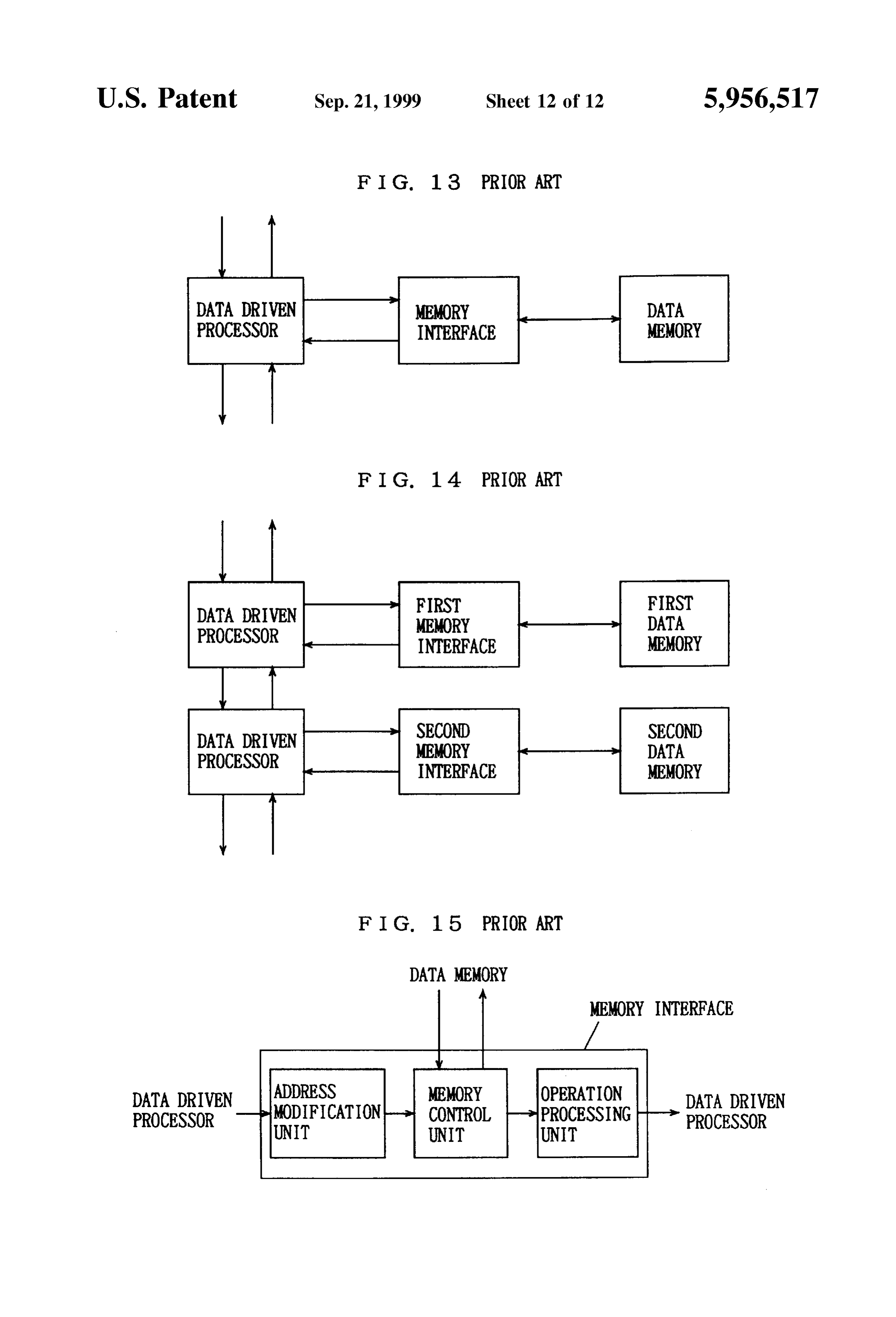
F I. G. 13 PRIOR ART
DATA DRIVEN MEMORY
PROCESSOR INTERFACE
F I. G. 14 PRIOR ART
INTERFACE
SECOND
DATA DRIVEN MEMORY
PROCESSOR INTERFACE
F I G. 15 PRIOR ART
DATA MEMORY
MEMORY INTERFACE
DATA DRIVEN
PROCESSOR
ges
MODIFICATION
MEMORY late
CONTROL PROCESSING
DATA DRIVEN
PROCESSOR
Page 14
DATA DRIVEN INFORMATION PROCESSOR not provided Separately, and therefore, there has been no facility which accesses data in each of the internal data
BACKGROUND OF THE INVENTION memory and the cache memory Simultaneously.
1. Field of the Invention In addition, the conventional data driven processor is not 5 provided with a function to Store a program in a memory
The present invention relates to a data driven information interface, and therefore, a data memory cannot be accessed processor, and more particularly, to a data driven informa without processing by a host processor (see FIG. 15). tion processor having a data driven type information pro Accordingly, frequent accesses to the data memory cause an cessing unit and a memory to be accessed upon execution of increase in load on the host processor, So that Speeding up of information processing by the processing unit, and capable the whole processing has been prevented.
of improving efficiency of access to the memory. SUMMARY OF THE INVENTION 2. Description of the Background Art
A data driven information processor is one type of non driven informationof processor
It is an object the present invention to provide a data
Von-Neumann computer having no concept of Sequential memories, which is capable ofhaving a plurality of a data increasing processing Speed, execution of instructions by a program counter. Such a data including access to each data memory.
driven information processor employs architecture based on In order to achieve this object, the data driven information parallel processing of instructions. In the data driven infor processor in accordance with the present invention includes mation processor, an execution of an instruction is enabled a processing upon a collection of data to be operated, and a plurality of processing theunit for receiving an applied data packet, instructions are simultaneously driven by data, So that pro outputting a data packetofwhich content the received data packet, and
Stores a result of the pro grams are executed in parallel in accordance with a natural cessing and Subsequent program data flow of the data. As a result, time required for operation will flow program; and a memory control of a first prestored data unit having a plurality be drastically reduced compared to the case of Von of data memories for Storing data to be referred to or updated Neumann computers. In order to further improve a proceSS upon execution of processing in the information processor ing Speed of the data driven information processor, the for inputting/outputting data to and from the processing
unit.
Speeding up of access to a memory (hereinafter referred to The memory control unit further includes an input unit for as a data memory) for storing data to be referred to or receiving, processing and outputting an applied data packet; updated upon execution of processing is desired.
FIG. 13 is a diagram showing the connection of a con input an acceSS unit for receiving a data packet output from the ventional data driven processor and an external data memories unit, accessing at least one of the plurality of data memory, and FIG. 14 is a diagram showing connection of a data packet,in and parallel based on the content of the received plurality of conventional data driven processors and external Stores a result of outputting the access the received data packet which upon each access to each data data memories. memory; an operation unit for receiving a data packet output FIG. 15 is a diagram showing a structure of a memory 35 from the access unit, operating the result of the acceSS in the interface for a conventional data driven processor. received data packet in accordance with the content of the In conventional data driven processors, a multi-processor received data packet, Storing a result of the operation in the System consisting of a plurality of processors and a plurality received data packet, and outputting the received data of memory interfaces is proposed in an article entitled "An packet; and a program Storage unit for receiving a data Evaluation of Parallel-Processing in the Dynamic Data 40 packet output from the operation unit and outputting a data Driven Processor”, pp. 9-18 issued on Nov. 12, 1991 in the packet which Stores both a result of the operation in the Micro Computer Architecture Symposium sponsored by received data packet and Subsequent program data in a Information Processing Society of Japan. Second prestored data flow program. In the conventional processor proposed therein, although According to the above described data driven information a data memory (hereinafter referred to as an internal data 45 processor, Since a plurality of data memories can be accessed memory) incorporated into the processor or a data memory in parallel by the acceSS unit of the memory control unit in (hereinafter referred to as an external data memory) located a single access time, improvement in a Speed of the entire external to the processor is connected to a Single memory processing, including access to each data memory, of the interface, data cannot be read/written from and to both information processor can be achieved. The memory control memories Simultaneously. In other words, Since the conven 50 unit Stores the Second data flow program in the program tional data driven processor allows an access to only one Storage unit, So that program control for access to a data data memory for one memory interface, only one data can be memory can be achieved independently of control of the accessed for a single access time (see FIG. 13). Accordingly, processing unit. Thus, the load on the processing unit is a double access time is required to acceSS data in both reduced, resulting in a higher processing Speed of the internal and external data memories, So that the Speeding up 55 processing unit.
of processing has been prevented. Since the input unit in the memory control unit of the In addition, in the conventional data driven processor, above described data driven information processor includes although an addresses of a data memory is modified by an address operation unit for calculating an address for address modification, addresses in a plurality of different parallel access by the access unit based on the content of a data memories cannot be modified using this address modi 60 data packet and on address modification data, address modi fication. Therefore, in order to access first and Second data fication for a plurality of data memories can be carried out. memories, first and Second memory interfaces for respec If the plurality of data memories include an external data tively accessing to the first and the Second memories are memory and one or more internal data memories, each required as shown in FIG. 14, thereby causing an increase in having a different acceSS Speed, parallel access to the exter cost and preventing a reduction in device size. 65 nal and the internal data memories as well as parallel access Furthermore, in the conventional data driven information to a plurality of internal data memories each having a processor, an internal data memory and a cache memory are different acceSS Speed can be performed.
Page 15
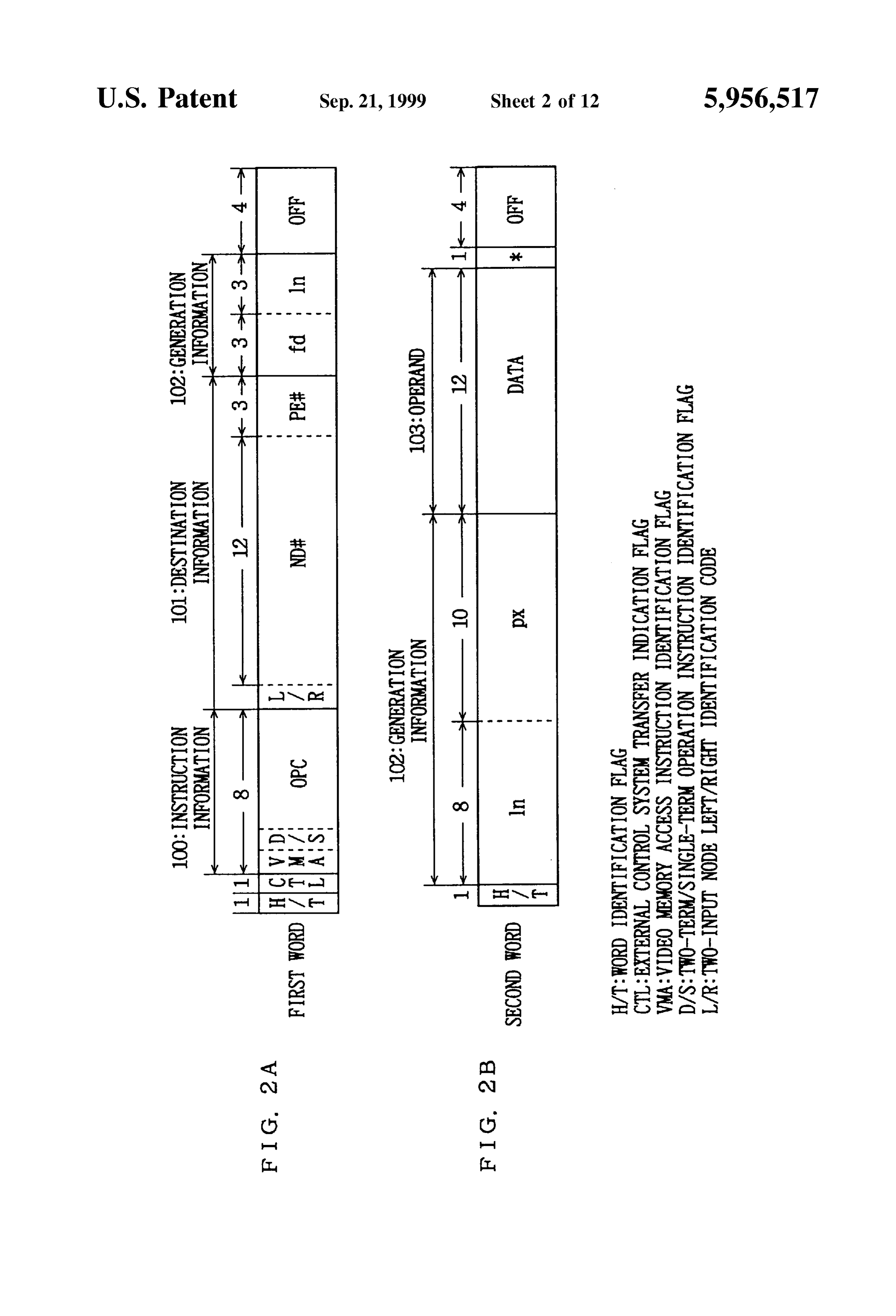
The foregoing and other objects, features, aspects and FIGS. 2A and 2B show a format of an I/O packet of the advantages of the present invention will become more data driven information processor of FIG. 1. apparent from the following detailed description of the Data to be processed in the data driven information present invention when taken in conjunction with the processor of FIG. 1 has a data packet Structure shown in accompanying drawings. FIGS. 2A and 2B. A packet for access to a video memory, BRIEF DESCRIPTION OF THE DRAWINGS which will be described later, is formed of two words each having 36 bits as shown in FIGS. 2A and 2B, and a packet
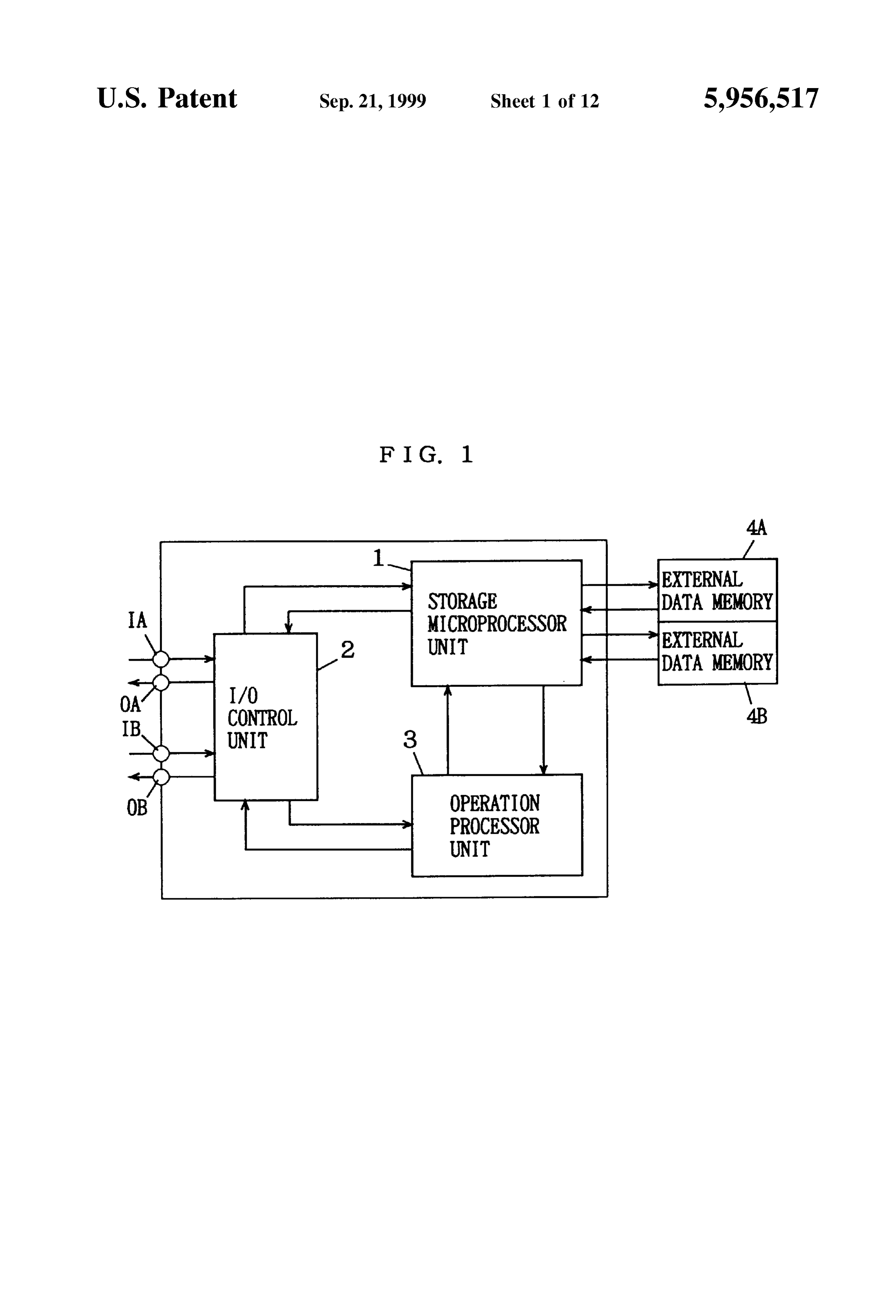
FIG. 1 is a diagram Schematically showing a structure of other than that packet is formed of two words each having a data driven information processor in accordance with an 32 bits without a generation offset OFF in FIGS. 2A and 2B. embodiment of the present invention. 1O A data packet stores instruction information 100, destination FIGS. 2A and 2B are diagrams showing a format of an I/O information 101, generation information 102 and an operand packet of the data driven information processor of FIG. 1. 103.
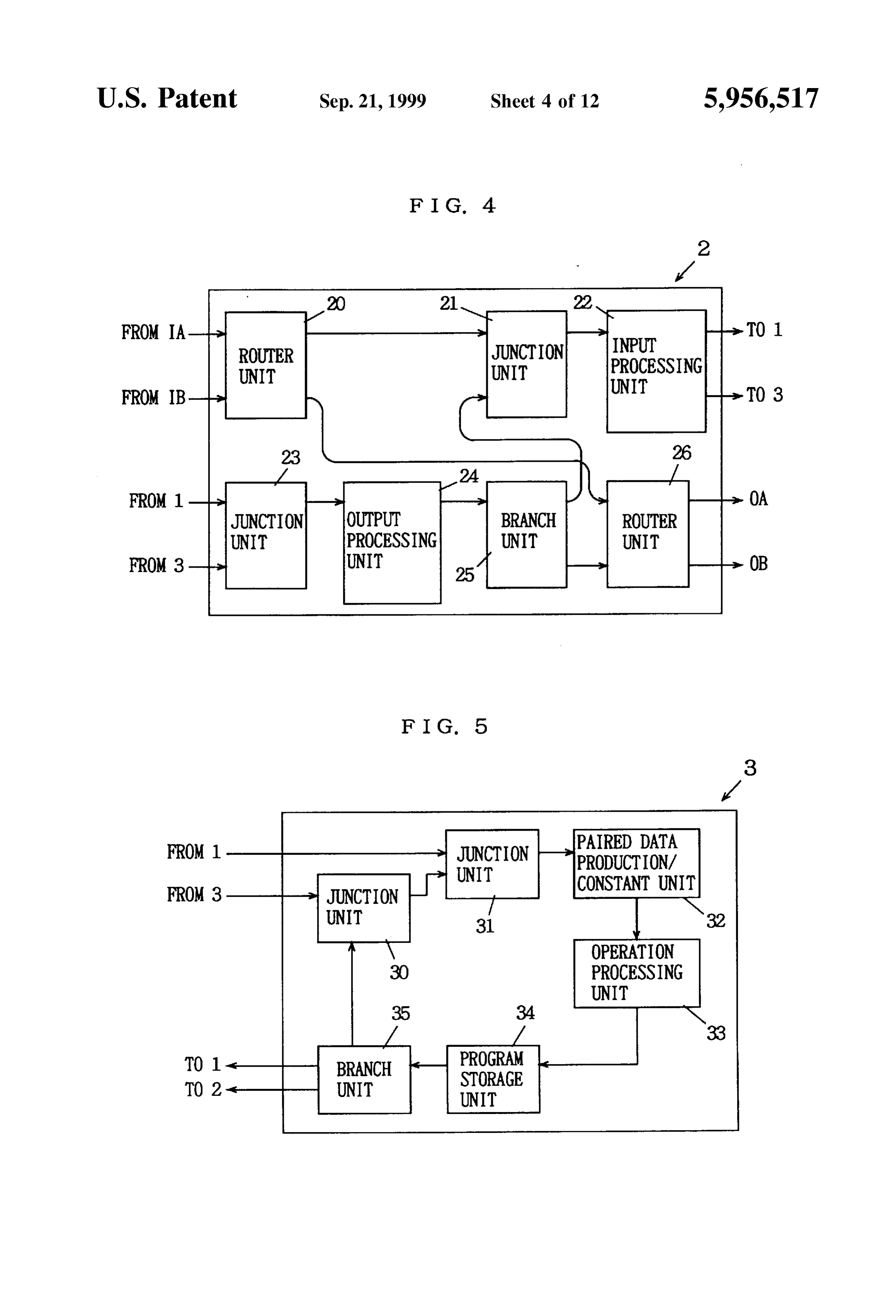
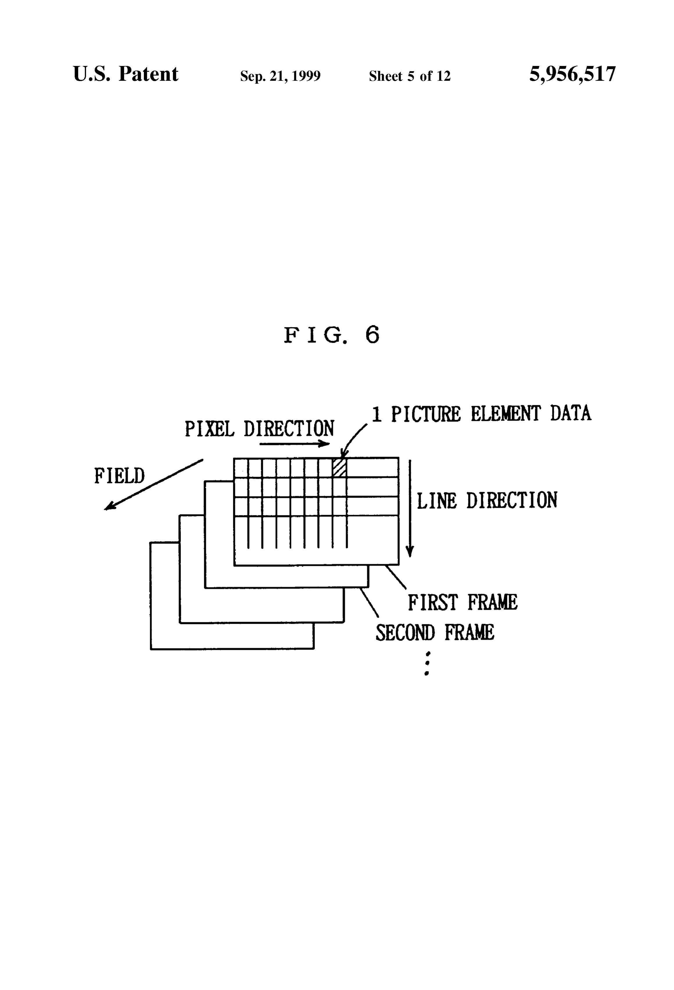
FIG. 3 is a diagram showing a structure of a Storage Instruction information 100 includes an operation code microprocessor unit in FIG. 1. OPC, and destination information 101 includes a node FIG. 4 is a diagram showing a structure of an I/O control 15 number ND# and a processor number PEii. unit in FIG. 1. Generation information 102 is information allotted when FIG. 5 is a diagram showing a structure of an operation the packet Stores time Series data for Video Signal processing processor unit in FIG. 1. or the like. Generation information 102 is allotted to a data FIG. 6 is a diagram showing a structure of image data in packet in accordance with the input-time order to the infor accordance with an embodiment of the present invention. mation processor. Generation information 102 is used as an FIGS. 7A and 7B are diagrams illustrating access to an addressand for access to a video memory as will be described internal data memory and an external data memory in below, address in includes a 3-bit field address fd, an 11-bit line and a 10-bit pixel address pX. Operand 103 accordance with an embodiment of the present invention.
FIG. 8 is a diagram illustrating Simultaneous access to tion code OPC. data DATA which is processed with opera
includes operand internal and external data memories in accordance with is an embodiment of the present invention. The data driven information processor of FIG. 1 includes a storage microprocessor unit 1, an I/O control unit 2 having
FIGS. 9A and 9B are diagrams illustrating access to input ports IA and IB and output ports OA and OB for addresses of the same line of an internal data memory and controlling input/output of a data packet to and from the a data cache in accordance with an embodiment of the processor, and an operation processor unit 3, and externally present invention. connects with external data memories 4A and 4.B. FIGS. 10A and 10B are diagrams illustrating access to I/O control unit 2 receives a data packet eXternally, and addresses of the same pixel of an internal data memory and outputs the data packet to Storage microprocessor unit 1 or a data cache in accordance with an embodiment of the 35 operation processor unit 3. Storage microprocessor unit 1 present invention. performs reading/writing from and to each type of data FIGS. 11A and 11B are diagrams illustrating access to memory and operation processing accompanying the addresses of the same line of an external data memory and reading/writing, and is able to access an internal data an internal data memory in accordance with an embodiment memory and an external data memory (4A, 4B) which will of the present invention. 40 be described below. Operation processor unit 3 is similar to FIGS. 12A and 12B are diagrams illustrating access to that in the conventional data driven processor. addresses of the Same pixel of an external data memory and A data packet input through I/O control unit 2 to the an internal data memory in accordance with an embodiment information processor is processed in accordance with a data of the present invention. flow program Stored in each of Storage microprocessor unit FIG. 13 is a diagram showing connection a between a 45 1 and operation processor unit 3. In this case, the data packet conventional data driven processor and an external data may be output from Storage microprocessor unit 1 to opera memory. tion processor unit 3, or may be output from operation FIG. 14 is a diagram showing connection a between a processor unit 3 to Storage microprocessor unit 1, depending plurality of conventional data driven processors and external on the processing of the program. The data packet which has data memories. 50 been processed within the information processor is output to FIG. 15 is a diagram showing a structure of a memory the outside of the information processor from I/O control interface for a conventional data driven processor. unit 2.
DESCRIPTION OF THE PREFERRED
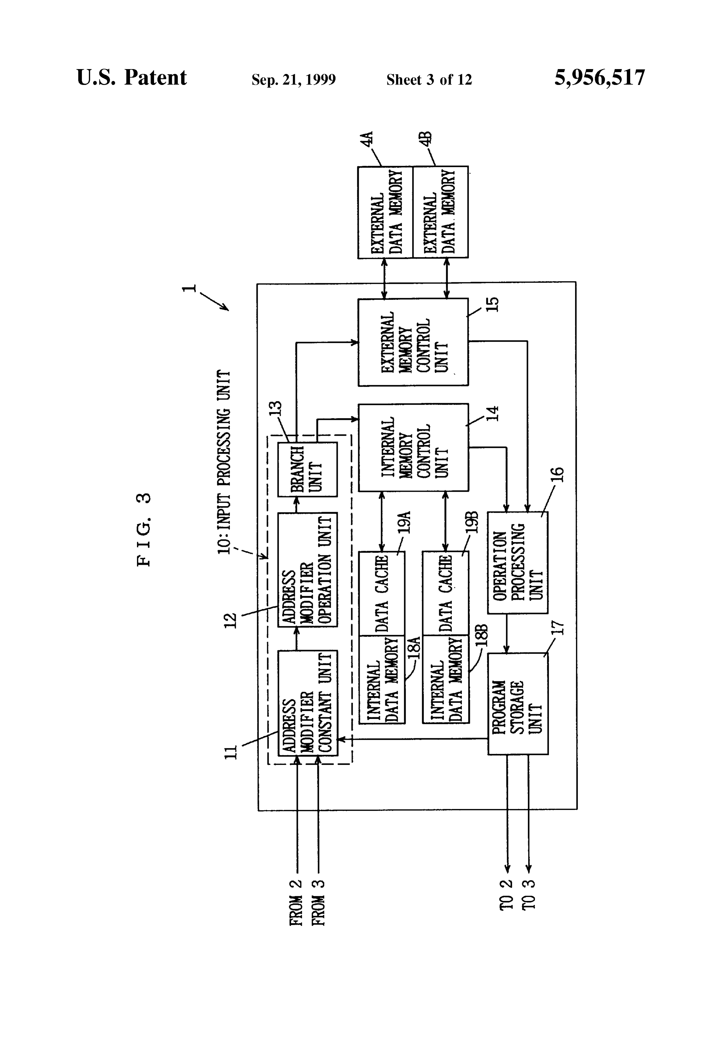
FIG. 3 shows a Structure of Storage microprocessor unit 1
EMBODIMENTS
of FIG.1. Storage microprocessor unit 1 of FIG. 3 includes 55 an input processing unit 10 for processing and outputting a
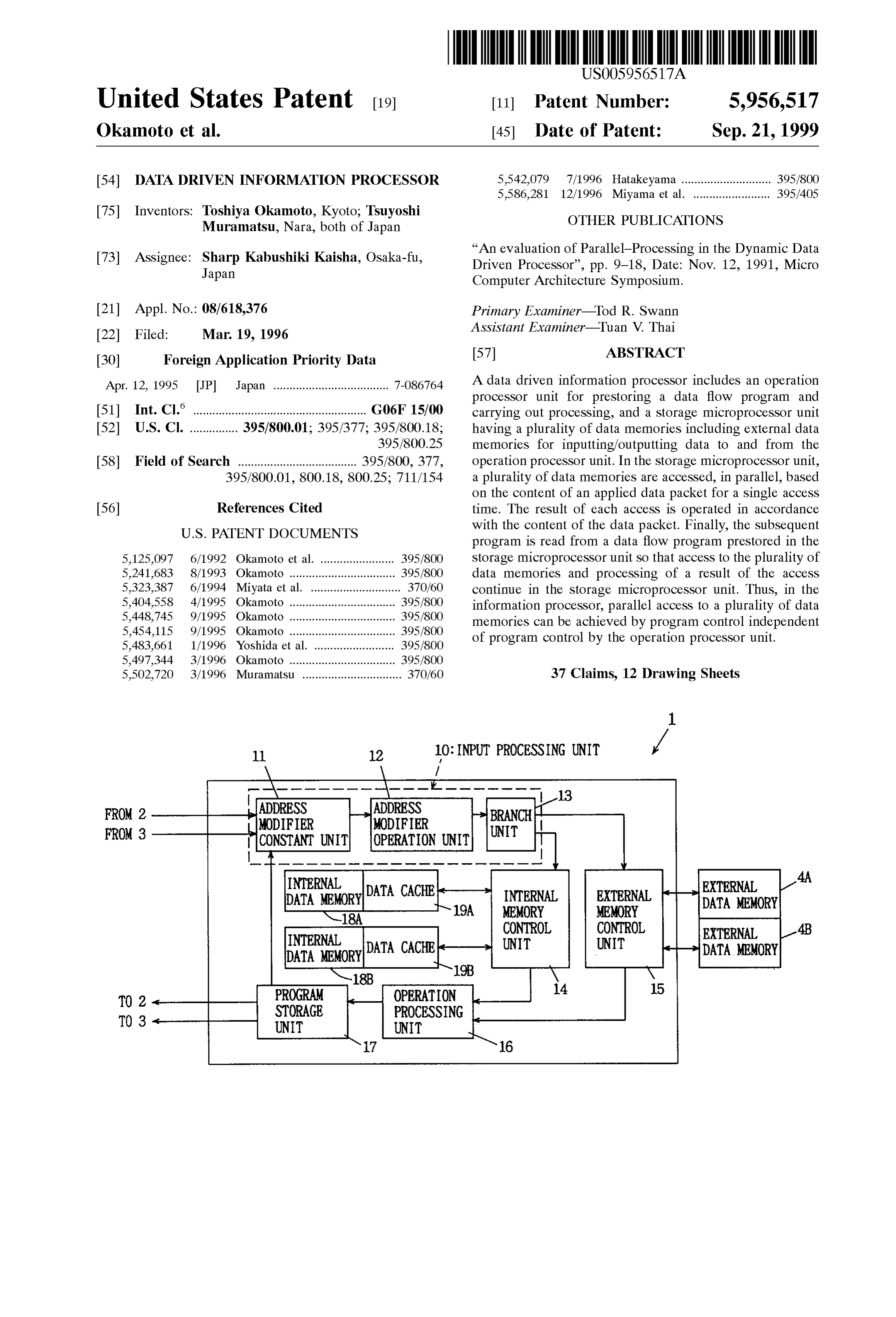
An embodiment of the present invention will now be data packet received from I/O control unit 2 or operation described in conjunction with the accompanying drawings. processor unit 3; an internal memory control unit 14 for In the following description, a data cache indicates a controlling access to internal data memories 18A and 18B as memory with Smaller capacity than internal and external well as data caches 19A and 19B; an external memory data memories, which can be accessed at a higher Speed than 60 control unit 15 for controlling access to external data memo those memories. Further, an internal data memory indicates ries 4A and 4B, an operation processing unit 16; and a a memory with Smaller capacity than an external data program Storage unit 17 for prestoring a data flow program memory, which can be accessed at a higher speed than the mainly for access to a data memory and processing of the external data memory. acceSS result.
FIG. 1 schematically shows a structure of a data driven 65 Input processing unit 10 includes an address modifier information processor in accordance with an embodiment of constant unit 11, an address modifier operation unit 12 and the present invention. a branch unit 13. An external data memory, an internal data
Page 16
S 6 memory and a data cache are prepared to make one Set as So as to output the data packet to router unit 26 if the shown in the figure, Since memories in each Set are accessed destination information 101 indicates the outside of the (interleaved) alternately on a one-by-one basis So as to information processor, and to output the data packet to achieve high-speed access to a memory. junction unit 21 if the destination information 101 indicates Address modifier constant unit 11 includes a memory (not the inside of the information processor. Junction unit 23 shown) for prestoring at least one constant value for address microprocessorreceives
Sequentially data packets applied from Storage modification. Upon receiving a data packet, constant unit 11 outputs a data packet toand unit 1 operation processor unit 3 and output processing unit 24.
reads a constant value from the memory based on the content Output processing unit 24 converts a data packet received of the received data packet to Store the constant value in the from received data packet as a generation offset OFF, and outputs formatjunction of the unit 23 from a data packet having a data inside of the information processor into a data the packet. packet having a data format of the outside of the information Based on an operation code OPC of the data packet, processor to output the resultant data packet to branch unit address modifier operation unit 12 calculates an address for 25. If destination information 101 of the data packet accessing each memory from a constant value of generation received from output processing unit 24 indicates the outside offset OFF and an address value (generation information 15 of the information processor, branch unit 25 outputs the 102) in the data packet applied from constant unit 11; Stores received data packet to router unit 26, and if the destination the address resulting from the calculation in the data packet information 101 indicates the inside of the information as generation information 102, and outputs the data packet processor, branch unit 25 outputs the received data packet to to branch unit 13. junction unit 21.
Based on instruction information 100 of the data packet, Router unit 26 outputs the data packet received from branch unit 13 outputs the data packet to internal memory router unit 20 or branch unit 25 to the outside of the control unit 14 if it determines that an address to be accessed information processor through either output port OA or OB, is an address of an internal memory (memories 18A and 18B based on destination information 101 of the received data or data caches 19A and 19B), outputs the data packet to 25 packet. Junction unit 21 Sequentially receives data packets external memory control unit 15 if it determines that an applied from branch unit 25 and router unit 20 to output a address to be accessed is an address of external data memo data packet to input processing unit 22. Input processing unit ries 4A and 4B, and outputs the data packet in parallel to 22 converts the data packet received from junction unit 21 internal memory control unit 14 and external memory con from a packet having a data format of the outside of the trol unit 15 if it determines that an address to be accessed is information processor into a data packet having a data both an address of internal memories (memories 18A and format of the inside of the information processor, and 18B, or data caches 19A and 19B) and an address of external outputs the resultant data packet either Storage micropro data memories 4A and 4.B. ceSSor unit 1 or operation processor unit 3 based on desti Then, the data packet which Stores, as an operand 103, the nation information 101 of the packet. result of access to a corresponding data memory through 35 FIG. 5 shows a structure of operation processor unit 3 of each control unit is output to operation processing unit 16. FIG. 1. In the figure, operation processor unit 3 includes Operation processing unit 16 operates corresponding oper junction units 30 and 31, a paired data production/constant and 103 based on an operation code OPC of the data packet, unit 32, an operation processing unit 33, a program Storage Stores the data of the result of the operation in the data packet unit 34 and a branch unit 34. Since the data processing in as operand 103 and outputs the packet to program Storage 40 paired data production/constant unit 32, operation process unit 17. Operation processing unit 16 only performs an ing unit 33 and program Storage unit 34 is described in detail operation of data obtained by access to a memory, and an in the above mentioned article “An Evaluation of Parallel operation other than that is carried out in operation processor Processing in the Dynamic Data Driven Processor”, a unit 3. description of which will be given briefly herein. Program Storage unit 17 reads the Subsequent program 45 Junction unit 30 Sequentially receives data packets data from the prestored data flow program in accordance applied from I/O control unit 2 and branch unit 33 and with the content of the data packet received from operation outputs a data packet to junction unit 31. Junction unit 31 processing unit 16, and Stores the program data in the data Sequentially receives data packets applied from junction unit packet. Then, program Storage unit 17 outputs the data 30 and Storage microprocessor unit 1 and outputs a data packet to address modifier constant unit 11 if destination 50 packet to paired data production/constant unit 32. information 101 in the received data packet indicates the Paired data production/constant unit 32 Sequentially inside of Storage microprocessor unit 1, and outputs the data receives data packets applied from junction unit 31, and packet to operation processor unit 3 external to Storage produces a pair of operand data DATA which can be microprocessor unit 1 if destination information 101 in the operated, or produces, if constant data corresponding to the received data packet indicates operation processor unit 3. If 55 received data packet is prestored in the constant unit, a pair destination information 101 indicates the outside of the data of operant data DATA of the received data packet and the driven information processor, the received data packet is constant data. The data pair produced is Stored in the output to the outside of the information processor through received data packet as operand data DATA, and the data I/O control unit 2. packet is output to operation processing unit 33. FIG. 4 shows a structure of I/O control unit 2 of FIG. 1. 60 Operation processing unit 33 receives the data packet In the figure, I/O control unit 2 includes router units 20 and output from paired data production/constant unit 32, pro 26 for controlling a path of a data packet, junction units 21 ceSSes a data pair in the received packet in accordance with and 23, an input processing unit 22, a branch unit 25 and an instruction information 100 in the received packet, and output processing unit 24. outputs the data packet which Stores data of the result as Router unit 20 receives a data packet applied from the 65 operand data DATA to program Storage unit 34. outside of the information processor through an input port Program Storage unit 34 prestores a data flow program. IA or IB and identifies destination information 101 thereof When program Storage unit 34 receives the data packet
Page 17
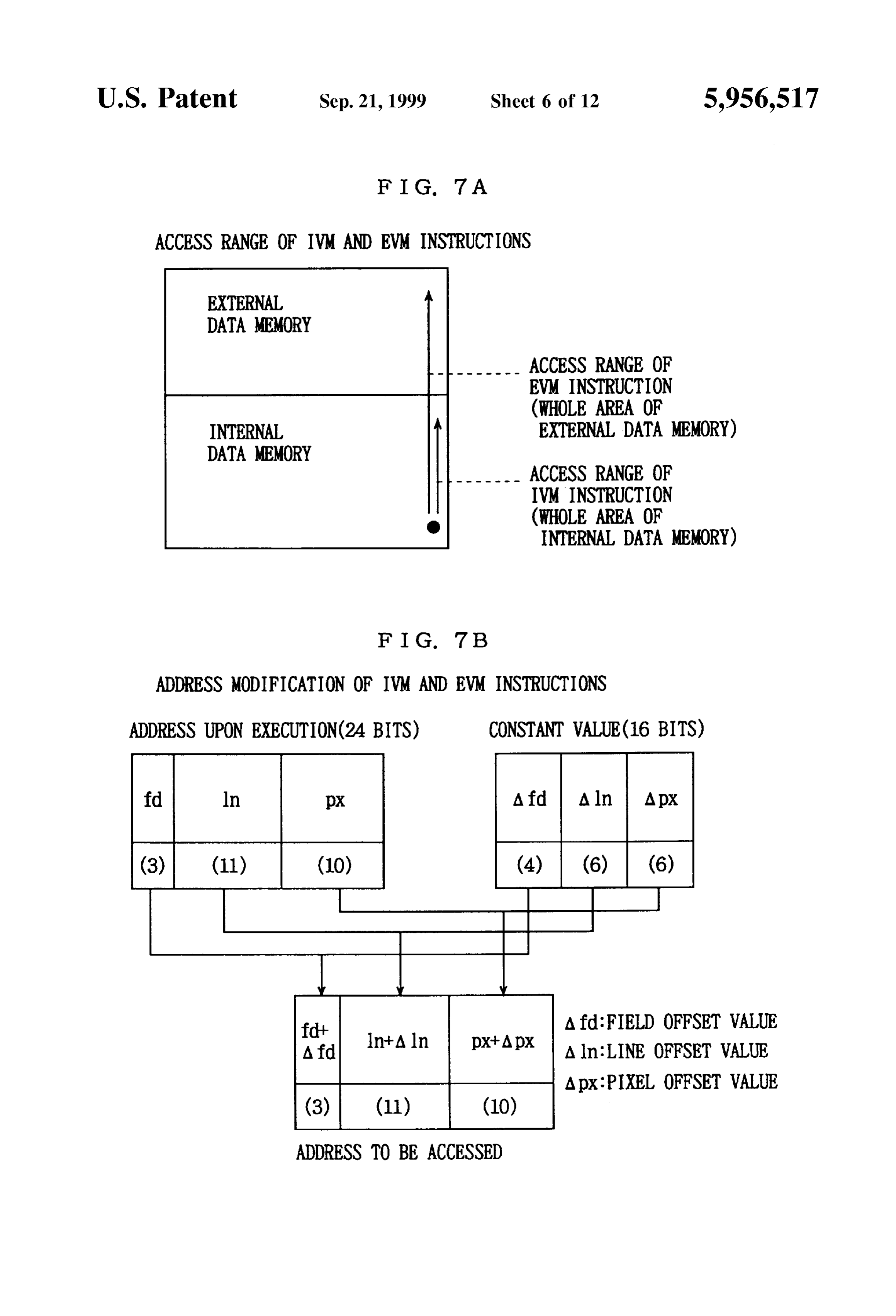
applied from operation processing unit 33, it reads the FIGS. 7A and 7B are diagrams illustrating access to an Subsequent program data from the program based on a node internal data memory and an external data memory in number ND# and generation information 102 of the received accordance with an embodiment of the present invention. data packet, Stores the program data in the received packet, FIG. 7A shows an example of access to internal data and outputs the packet to branch unit 35. memory 18A or 18B. An IVM (Internal Video Memory) When branch unit 35 receives the data packet applied instruction is Set in an operation code OPC for carrying out from program Storage unit 34, it outputs the data packet to this access. The whole area of internal data memory 18A or either junction unit 30, Storage microprocessor unit 1 or I/O 18B can be accessed in accordance with the IVM instruc control unit 2 based on destination information 101 thereof. tion.
Storage microprocessor unit 1 has program Storage unit In addition, FIG. 7A shows an example of access to 17 as shown in FIG. 3, so that control of a program for external data memory 4A or 4.B. An EVM (External Video access to a data memory in the information processor can be Memory) instruction is set in an operation code OPC for performed independently of control of a program Stored in carrying out this access. The whole area of external data program Storage unit 34 of operation processor unit 3. memory 4A or 4B can be accessed in accordance with the Accordingly, Since operation processing by the operation 15 EVM instruction.
processor unit 3 and access to a data memory by the Although the Same address for access is used in both the microprocessor unit 1 can be carried out in parallel, load on IVM instruction and the EVM instruction, the internal data the operation processor unit 3 is reduced and processing memory and the external data memory are provided Sepa Speed in the information processor is improved compared to rately as shown in FIG.3, So that access thereto is carried out a conventional example. Separately.
Storage microprocessor unit 1 includes input processing FIG. 7B shows a relationship between an address and an unit 10, internal memory control unit 14 and external address modification value (hereinafter referred to simply as memory control unit 15, So that parallel access to data a constant value) of address modifier constant unit 11. An memories 18A and 18B, data caches 19A and 19B and 25 address upon execution is indicated by a field address fd, a external data memories 4A and 4B can be performed for a line address in and a pixel address pX in a data memory. Single access time. This access to a memory will now be Picture element data in the data memory can be accessed by described in detail using, as an example, image data pro generation information 102.
cessing which particularly requires high Speed processing An address (fd, lin, px) upon execution is converted into and handles a large amount of data, assuming that internal an address of internal data memory 18A or 18B and external and external data memories are video memories. data memory 4A or 4B in address modifier operation unit 12, FIG. 6 is a diagram showing a structure of image data in using a constant value (a field offset value Afd, a line offset accordance with an embodiment of the present invention. AS value Aln, a pixel offset value Apx) applied by address shown in the figure, image data consists of a plurality of modifier constant unit 11 of FIG.3 as an offset value. Then, frames (fields), each frame is constituted by a plurality of 35 each data memory is accessed through internal memory picture element data arranged two-dimentionally (in pixel control unit 14 or external memory control unit 15 based on and line directions), and each picture element data in image the address (fd-i-Afd, lin+Aln, pX--Apx) obtained by conver data is identified (addressed) uniquely on a data memory by SO.
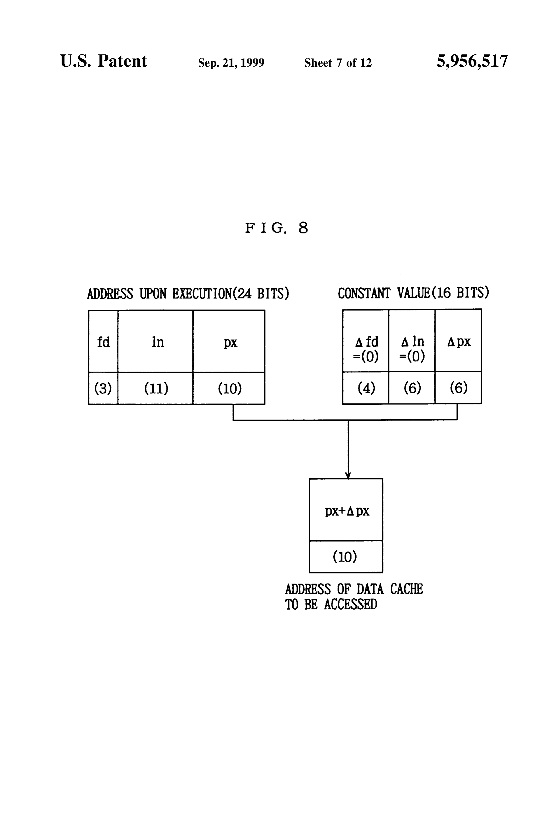
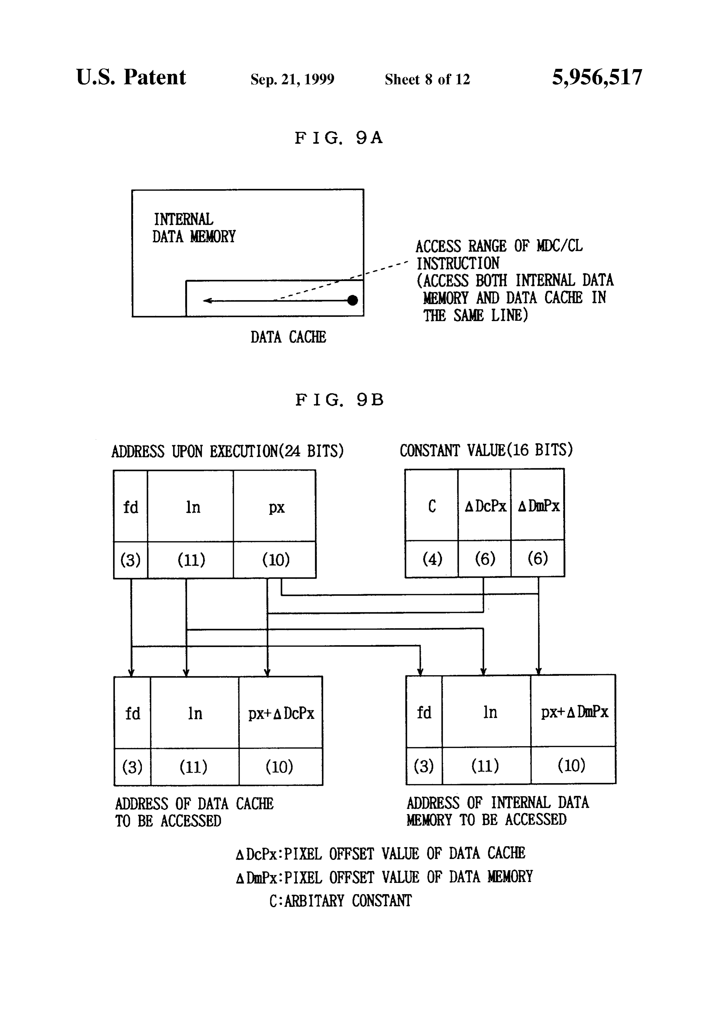
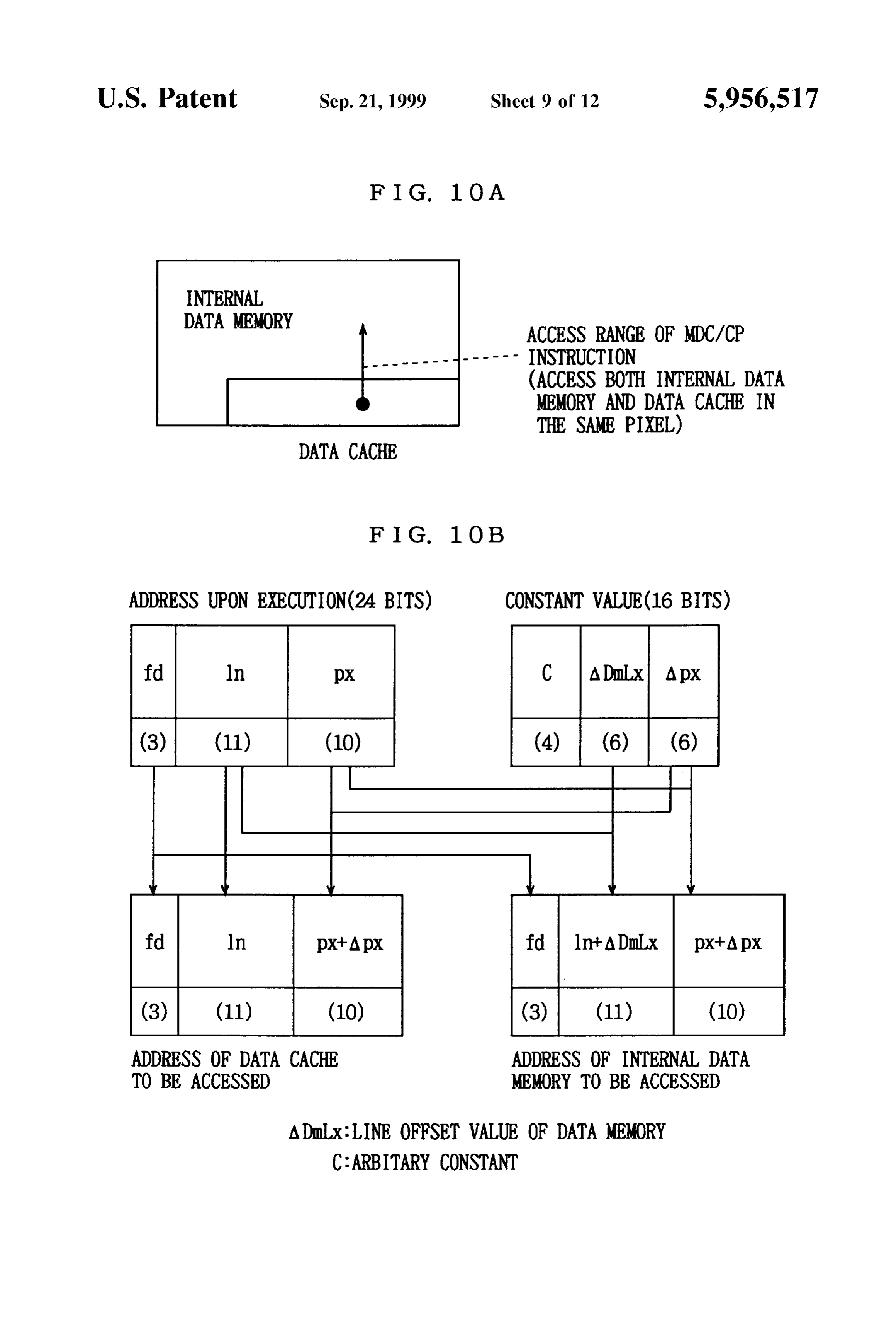
an address (field, pixel direction, line direction). FIG. 8 is a diagram illustrating Simultaneous access to an Characteristic processing of image data processing 40 internal data memory and an external data memory in includes filtering processing. In the filtering processing, a accordance with an embodiment of the present invention. A comparison between data adjacent to each other in the pixel CPX (ALU for Complex operation) instruction is set in an direction, a comparison between data adjacent to each other operation code OPC for carrying out this access. Since only in the line direction, and the comparison between fields a pixel offset value Apx of the constant value is valid in the adjacent to each other are carried out for picture element 45 CPX instruction, data cache 19A or 19B is accessed. data. In this case, information on picture element data in the FIGS. 9A and 9B are diagrams illustrating access to pixel direction of image data is Stored in data caches 19A addresses of the same line of an internal data memory and and 19B, information on picture element data in the line a data cache in accordance with an embodiment of the direction of image data is Stored in internal data memories present invention. An MDC/CL (Multiple access with Data 18A and 18B, and information on a field of image data is 50 Cache in Common Line) instruction is Set in an operation stored in external data memories 4A and 4.B. It is herein code OPC for carrying out this access. Since a pixel offset noted that a pixel address pX is used to identify picture value ADmPx of an internal data memory and a pixel offset element data in the pixel direction of a data memory, a line value ADcPX of a data cache are included in a constant value address ln is used to identify picture element data in the line in the MDC/CM instruction, separate pixel addresses px for direction on a data memory, and a field address fd is used to 55 internal data memory 18A or 18B and data cache 19A or 19B identify picture element data by field. Access to a memory are accessed. In this case, an offset value Aln for a line in accordance with the present embodiment will now be address ln is not included in the constant value. described with reference to FIGS. 7 to 12. FIGS. 10A and 10B are diagrams illustrating access to It is noted that a constant value (16 bits) of FIGS. 7 to 12 addresses of the Same pixel of an internal data memory and is applied as a generation offset OFF to address modifier 60 a data cache in accordance with an embodiment of the operation unit 12 by address modifier constant unit 11 of present invention. An MDC/CP (Multiple access with a Data FIG. 3. Operation of calculating an address to be accessed Cache in Common Pixel) instruction is set in an operation from an address (24 bits) upon execution indicated by code OPC for carrying out this access. Since only an offset generation information 102 and from a constant value (16 value ADmLX for a line address ln of internal data memory bits), Storing the calculated address in a data packet as 65 18A or 18B is included in a constant value in the MDC/CP generation information 102 and outputting the data packet is instruction, a line address ln of internal data memory 18A or carried out by address modifier operation unit 12. 18B is accessed. In this case, a pixel offset value APX for a
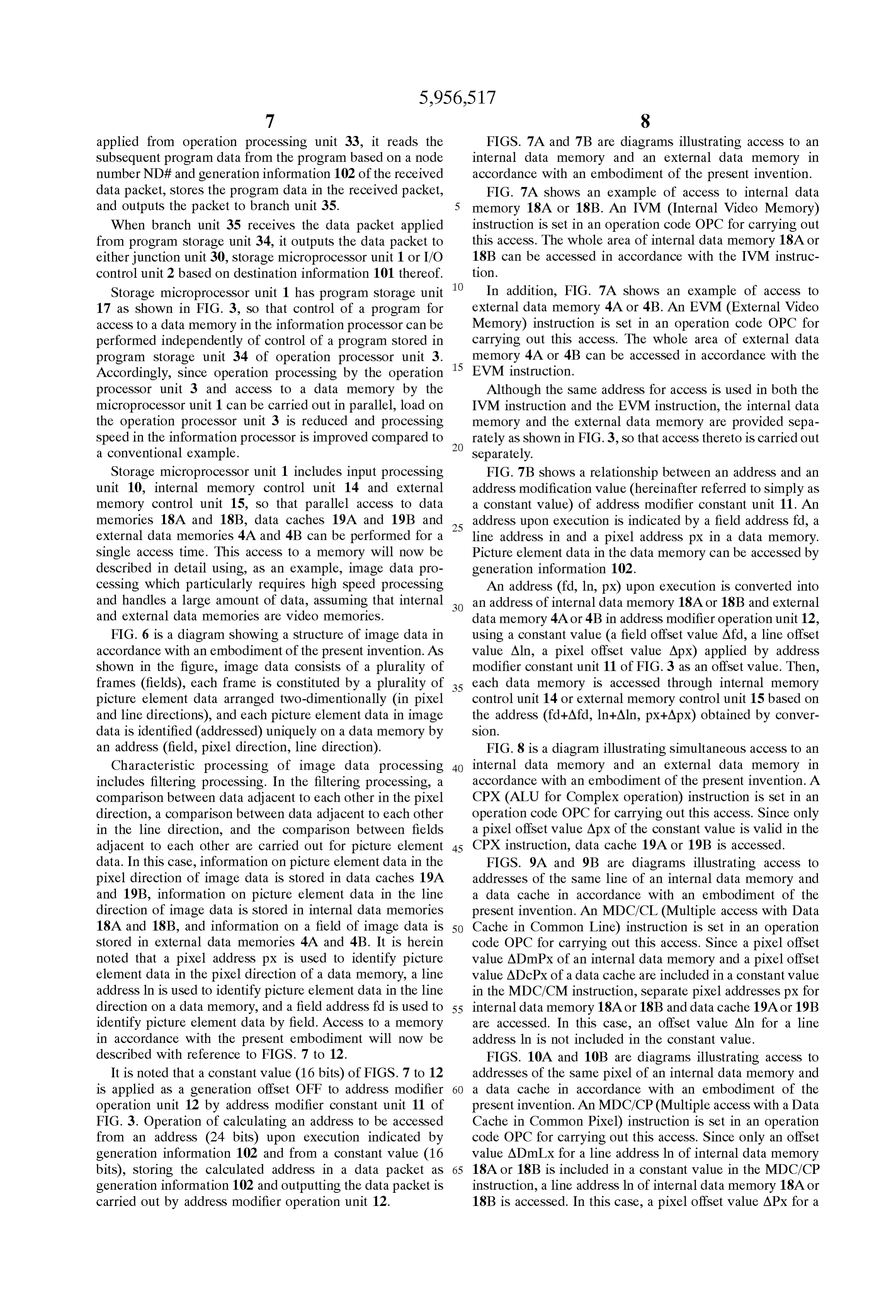
Page 18
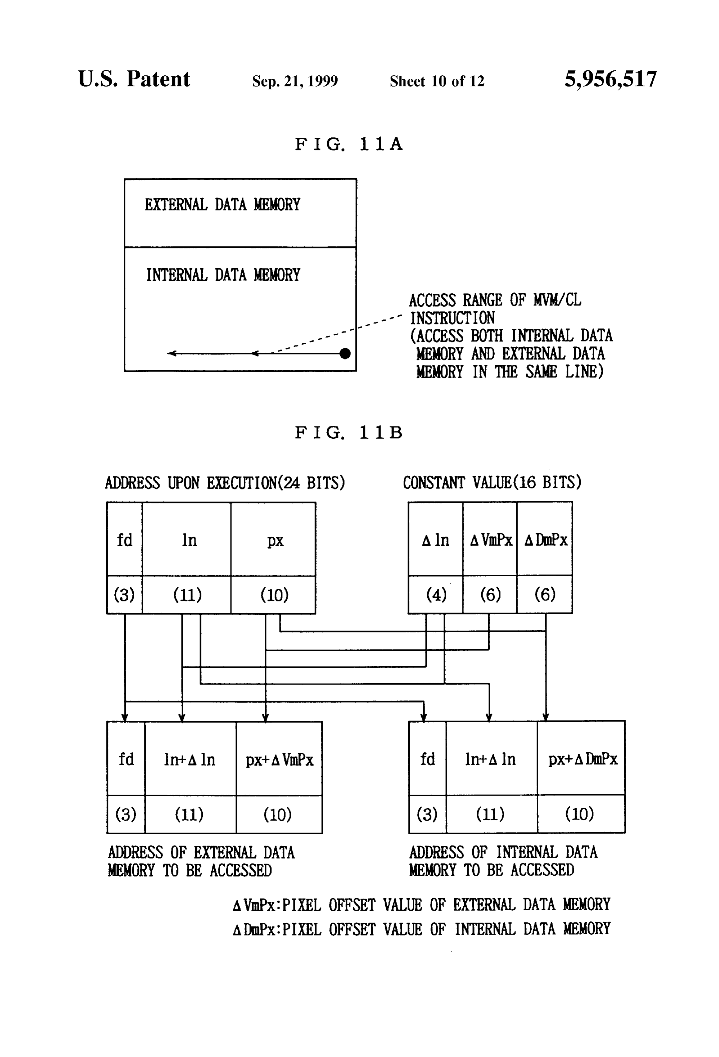
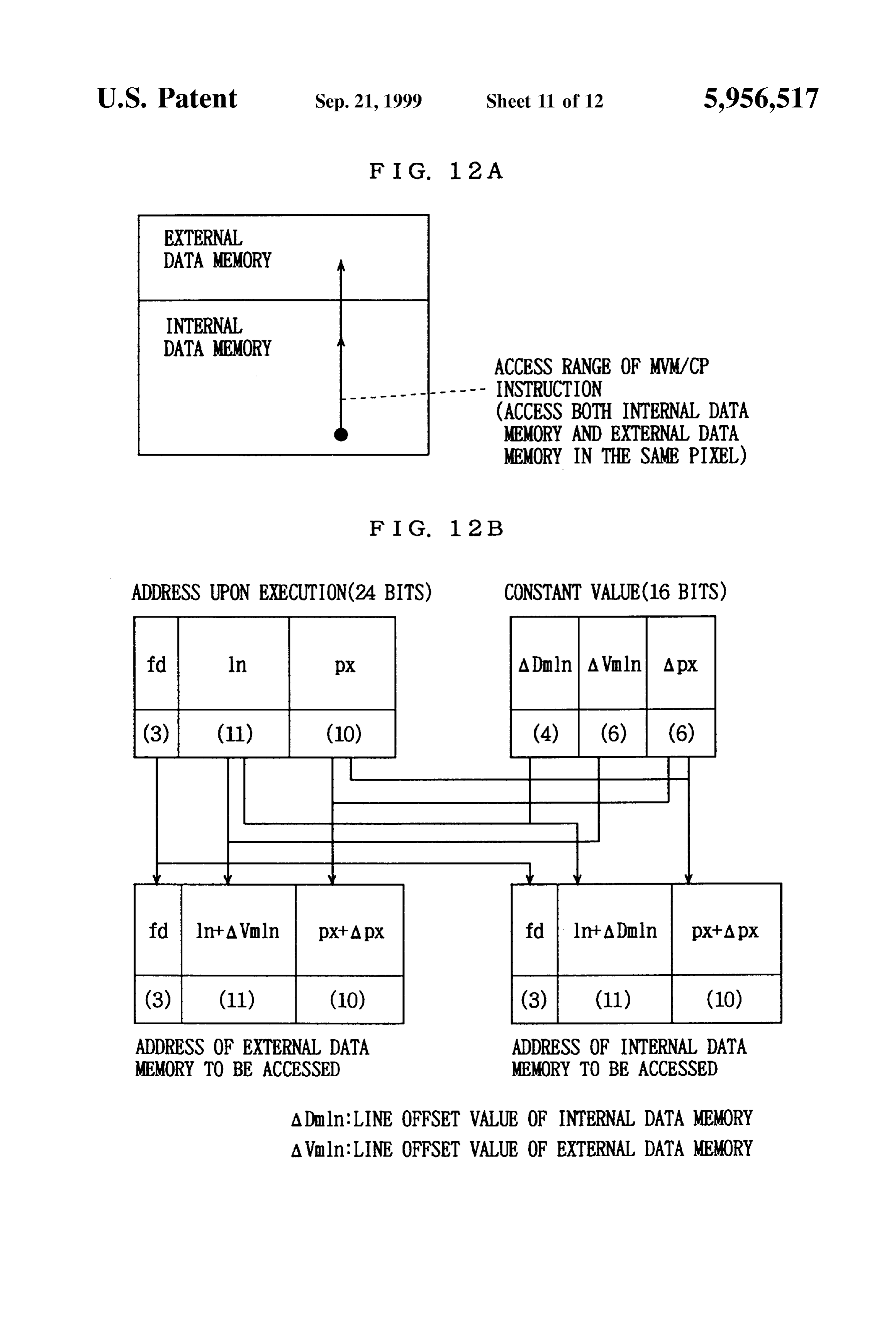
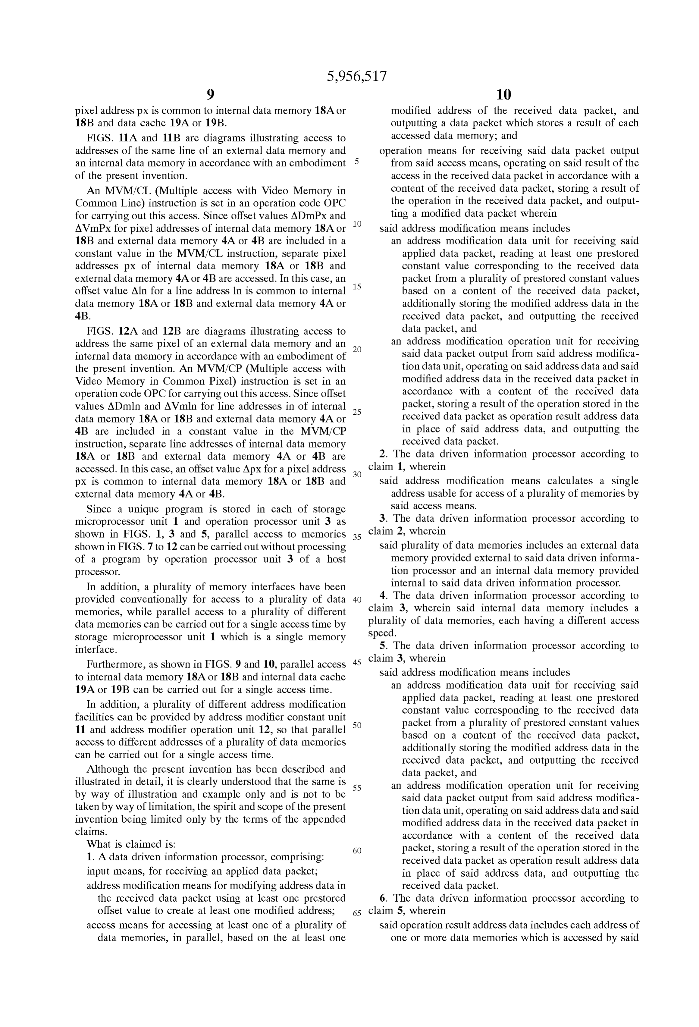
pixel address pX is common to internal data memory 18A or modified address of the received data packet, and 18B and data cache 19A or 19B. outputting a data packet which Stores a result of each FIGS. 11A and 11B are diagrams illustrating access to accessed data memory; and addresses of the same line of an external data memory and operation means for receiving Said data packet output an internal data memory in accordance with an embodiment from Said acceSS means, operating on Said result of the of the present invention. acceSS in the received data packet in accordance with a An MVM/CL (Multiple access with Video Memory in content of the received data packet, Storing a result of Common Line) instruction is set in an operation code OPC the operation in the received data packet, and output for carrying out this access. Since offset values ADmPX and ting a modified data packet wherein AVmPx for pixel addresses of internal data memory 18A or Said address modification means includes 18B and external data memory 4A or 4B are included in a an address modification data unit for receiving Said constant value in the MVM/CL instruction, separate pixel applied data packet, reading at least one prestored addresses px of internal data memory 18A or 18B and constant value corresponding to the received data external data memory 4A or 4B are accessed. In this case, an 15 packet from a plurality of prestored constant values offset value Aln for a line address ln is common to internal based on a content of the received data packet, data memory 18A or 18B and external data memory 4A or additionally storing the modified address data in the 4B. received data packet, and outputting the received FIGS. 12A and 12B are diagrams illustrating access to data packet, and address the same pixel of an external data memory and an an address modification operation unit for receiving internal data memory in accordance with an embodiment of Said data packet output from Said address modifica the present invention. An MVM/CP (Multiple access with tion data unit, operating on Said address data and Said Video Memory in Common Pixel) instruction is set in an modified address data in the received data packet in operation code OPC for carrying out this access. Since offset accordance with a content of the received data values ADmln and AVmln for line addresses in of internal 25 packet, Storing a result of the operation Stored in the data memory 18A or 18B and external data memory 4A or received data packet as operation result address data 4B are included in a constant value in the MVM/CP in place of Said address data, and outputting the instruction, Separate line addresses of internal data memory received data packet.
18A or 18B and external data memory 4A or 4B are 2. The data driven information processor according to accessed. In this case, an offset value Apx for a pixel address claim 1, wherein px is common to internal data memory 18A or 18B and Said address modification means calculates a single external data memory 4A or 4.B. address usable for access of a plurality of memories by Since a unique program is stored in each of storage Said access means.
microprocessor unit 1 and operation processor unit 3 as 3. The data driven information processor according to shown in FIGS. 1, 3 and 5, parallel access to memories 35 claim 2, wherein shown in FIGS. 7 to 12 can be carried out without processing Said plurality of data memories includes an external data of a program by operation processor unit 3 of a host memory provided external to Said data driven informa processor. tion processor and an internal data memory provided In addition, a plurality of memory interfaces have been internal to Said data driven information processor. provided conventionally for access to a plurality of data 40 4. The data driven information processor according to memories, while parallel access to a plurality of different claim 3, wherein Said internal data memory includes a data memories can be carried out for a single access time by plurality of data memories, each having a different acceSS Storage microprocessor unit 1 which is a Single memory Speed.
interface. 5. The data driven information processor according to Furthermore, as shown in FIGS. 9 and 10, parallel access 45 claim 3, wherein
Said address modification means includes to internal data memory 18A or 18B and internal data cache 19A or 19B can be carried out for a single access time. an address modification data unit for receiving Said applied data packet, reading at least one prestored
In addition, a plurality of different address modification constant value corresponding to the received data facilities can be provided by address modifier constant unit 50 packet from a plurality of prestored constant values 11 and address modifier operation unit 12, So that parallel based on a content of the received data packet, access to different addresses of a plurality of data memories additionally storing the modified address data in the can be carried out for a single access time. received data packet, and outputting the received Although the present invention has been described and data packet, and illustrated in detail, it is clearly understood that the same is 55 an address modification operation unit for receiving by way of illustration and example only and is not to be Said data packet output from Said address modifica taken by way of limitation, the Spirit and Scope of the present tion data unit, operating on Said address data and Said invention being limited only by the terms of the appended modified address data in the received data packet in claims. accordance with a content of the received data What is claimed is: 60 packet, Storing a result of the operation Stored in the 1. A data driven information processor, comprising: received data packet as operation result address data input means, for receiving an applied data packet; in place of Said address data, and outputting the address modification means for modifying address data in received data packet.
the received data packet using at least one prestored 6. The data driven information processor according to offset value to create at least one modified address, 65 claim 5, wherein access means for accessing at least one of a plurality of Said operation result address data includes each address of data memories, in parallel, based on the at least one one or more data memories which is accessed by Said
Page 19
acceSS means in accordance with a content of Said data 14. The data driven information processor according to packet which Stores the operation result address data. claim 2, wherein 7. The data driven information processor according to an operation code is further Stored in Said data packet, and claim 6, wherein Said acceSS means accesses at least one of Said plurality of an operation code is further Stored in Said data packet, and data memories, in parallel, based on Said operation Said acceSS means accesses at least one of Said plurality code and based on Said operation result address data in of data memories, in parallel, based on Said operation Said data packet received from Said input means. 15. The data driven information processor according to code and based on Said operation result address data claim 14, wherein in Said data packet received from Said input means.
8. The data driven information processor according to 1O Said access means includes claim 7, wherein external acceSS means for accessing Said external data Said access means includes memory, and external access means for accessing Said external data internal access means for accessing Said internal data memory, and memory, and internal acceSS means for accessing Said internal data 15 Saidmeans input means further includes for outputting Said data packet to be output from memory, and
Said input means further includes the input means to at least one of Said external access means and Said internal access means based on Said means for outputting Said data packet to be output from operation code in the data packet. the input means to at least one of Said external access 16. The data driven information processor according to means and Said internal access means based on Said operation code in the data packet. claim 1, wherein 9. The data driven information processor according to Said plurality of data memories includes an external data claim 5, wherein memory provided external to Said data driven informa an operation code is further Stored in Said data packet, and 25 tion processor and an internal data memory provided internal to Said data driven information processor.
Said access means accesses at least one of Said plurality of 17. The data driven information processor according to data memories, in parallel, based on Said operation claim 16, wherein code and based on Said operation result address data in Said internal data memory includes a plurality of data Said data packet received from Said input means. memories, each having a different access Speed. 10. The data driven information processor according to 18. The data driven information processor according to claim 9, wherein claim 1, wherein
Said access means includes an operation code is further Stored in Said data packet, and external acceSS means for accessing Said external data said access means accesses at least one of Said plurality of memory, and data memories, in parallel, based on Said operation internal acceSS means for accessing Said internal data 35 code and based on Said operation result address data in memory, and Said data packet received from Said input means. Said input means further includes 19. The data driven information processor according to means for outputting Said data packet to be output from claim 18, wherein the input means to at least one of Said external access Said access means includes means and Said internal access means based on Said 40 operation code in the data packet. external acceSS means for accessing Said external data memory, and 11. The data driven information processor according to internal access means for accessing Said internal data claim 2, wherein memory, and
Said operation result address data includes each address of 45 Said input means further includes one or more data memories which is accessed by Said means for outputting Said data packet to be output from acceSS means in accordance with a content of Said data packet which Stores the operation result address data. the input means to at least one of Said external access means to Said internal acceSS means based on Said 12. The data driven information processor according to operation code in the data packet. claim 11, wherein 20. The data driven information processor according to an operation code is further Stored in Said data packet, and 50 claim 1, wherein
Said access means accesses at least one of Said plurality of Said operation result address data includes each address of data memories in parallel based on Said operation code one or more data memories which is accessed by Said and Said operation result address data in Said data acceSS means in accordance with a content of Said data packet received from Said input means. 55 packet which Stores the operation result address data. 13. The data driven information processor according to 21. The data driven information processor according to claim 12, wherein claim 20, wherein
Said access means includes an operation code is further Stored in Said data packet, and external access means for accessing Said external data Said acceSS means accesses at least one of Said plurality of memory, and 60 data memories, in parallel, based on Said operation internal access means for accessing Said internal data code and based on Said operation result address data in memory, and Said data packet received from Said input means. Said input means further includes 22. The data driven information processor according to means for outputting Said data packet to be output from claim 21, wherein the input means to at least one of Said external access 65 Said access means includes means and Said internal access means based on Said external acceSS means for accessing Said external data operation code in the data packet. memory, and
Page 20
internal acceSS means for accessing Said internal data and the at least one modified address is used to access a memory, and memory internal to the data driven information processor, in Said input means further includes parallel.
means for outputting Said data packet to be output from 30. A data driven processing method, comprising the Steps the input means to at least one of Said external access 5 of:
means and Said internal access means based on Said receiving an input data packet;
operation code in the data packet. modifying address data in the received data packet using 23. The data driven information processor according to at least one prestored offset value to create at least one claim 1, further comprising:
a processing unit for receiving the applied data packet modified address, from the input means, and for Outputting the applied accessing at least one of a plurality of memories, in data packet to the address modification means, the parallel, based upon the at least one modified address, applied data packet further Storing a first prestored data and outputting a data packet Storing data retrieved from flow program; and each memory access,
program Storage means for receiving the data packet operating on the data packet with the data retrieved from output from Said operation means, and outputting a data each memory access, and packet which Stores Said result of the operation in the outputting a modified data packet Storing a result the modified data packet and Subsequent program data in a operation, wherein Said Step of modifying address data Second prestored data flow program, includes the Substeps of,
Said Second data flow program being used for access of receiving Said applied data packet, Said plurality of data memories and for processing of reading at least one prestored constant value corre resultant data of Said access among Said information sponding to the received data racket from a plurality processing in Said data driven information processor, of prestored constant values based on a content of the and Said first data flow program being used for pro 25 received data packet data, cessing other than Said acceSS and Said processing of additionally Storing the modified address data in the resultant data of Said access. received packet, and 24. The data driven information processor according to outputting the received data packet to an address modi claim 23, wherein fication unit which receives the data packet and the destination information is further Stored in Said data modified address data in the received data packet in packet, accordance with a content of the received data Said processing unit outputs, based on Said destination packet, Stores a result of the operation Stored in the received data packet as operation result address data information in said data packet to be output from the in place of the address data, and outputs the received processing unit, the data packet to Said access means, data packet.
external to the data driven information processor and 35 internal to Said processing unit, or 31. The method of claim 30, wherein said plurality of memories include an external data memory provided exter to Said input means, external to the data driven informa nal to Said data driven processor and an internal data tion processor, or to Said processing unit. memory provided internal to Said data driven processor. 25. The data driven information processor according to 40 32. The method of claim 31, wherein the internal data claim 1, wherein memory includes a plurality of data memories with different Said plurality of data memories are image memories. acceSS Speed.
26. The data driven information processor of claim 1, 33. The method of claim 30, wherein the plurality of data wherein the address modification means creates at least two memories are image memories.
addresses, each used by the acceSS means to access, in 45 34. The method of claim 30, wherein at least two modified parallel, at least one data memory. addresses are created, each used, in parallel, to access at 27. The data driven information processor of claim 26, least one data memory.
wherein the at least two modified addresses are used to 35. The method of claim 34, wherein each at least one data access two memories internal to the data driven information memory is a memory internal to the data driven processor. processor, in parallel. 50 36. The method of claim 30, wherein at least one modified 28. The data driven information processor of claim 1, address is created which is used to access a plurality of wherein the address modification means creates at least one memories, in parallel.
modified address that is used to access a plurality of 37. The method of claim 36, wherein the plurality of memories, in parallel. memories include one memory external to and one memory 29. The data driven information processor of claim 28, 55 internal to the data driven processor.
wherein the at least one modified address is used to acceSS a memory external to the data driven information processor k k k k k
Provenance
- Collection
- Cited prior art
- Original PDF
- patentimages.storage.googleapis.com →
- Filed
- 1996-03-19
- Pages
- 20
- Method
- pdftotext (the PDF's own text layer) + pdftoppm 300dpi page scans
- Source
- Google Patents bibliographic record
- Granted
- 1999-09-21
- Inventors
- Toshiya Okamoto; Tsuyoshi Muramatsu; Sharp Corp
- Transcribed from
- patentimages.storage.googleapis.com →