patent · US5376185
Single-junction solar cells with the optimum band gap for terrestrial concentrator applications
27 December 1994
Page 1 — bibliographic record
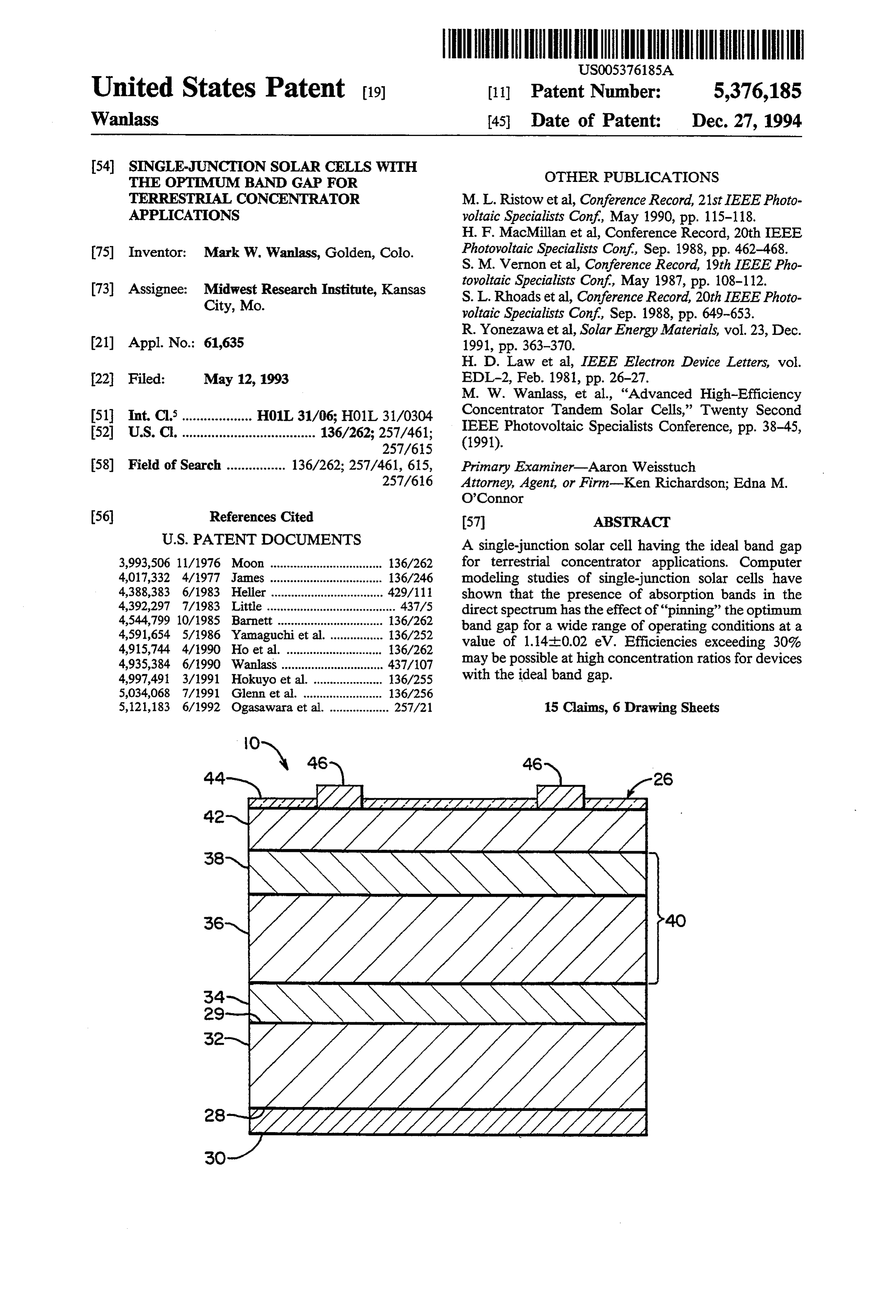
United States Patent (19) 11 Patent Number: 5,376,185 Wanlass (45) Date of Patent: Dec. 27, 1994 (54) SINGLE-JUNCTION SOLAR CELLS WITH OTHER PUBLICATIONS
THE OPTIMUM BAND GAP FOR
TERRESTRAL CONCENTRATOR M. L. Ristow etal, Conference Record, 21st IEEE Photo APPLICATIONS voltaic Specialists Conf, May 1990, pp. 115-118. H. F. MacMillan et al, Conference Record, 20th IEEE (75) Inventor: Mark W. Wanlass, Golden, Colo. Photovoltaic Specialists Conf, Sep. 1988, pp. 462-468. S. M. Vernon et al, Conference Record, 19th IEEE Pho (73) Assignee: Midwest Research Institute, Kansas tovoltaic Specialists Conf, May 1987, pp. 108-112. City, Mo. S. L. Rhoads etal, Conference Record, 20th IEEE Photo voltaic Specialists Conf, Sep. 1988, pp. 649-653.
R. Yonezawa et al, Solar Energy Materials, vol. 23, Dec.
21) Appl. No.: 61,635 1991, pp. 363-370.
H. D. Law et al, IEEE Electron Device Letters, vol.
(22) Filed: May 12, 1993 EDL-2, Feb. 1981, pp. 26-27. M. W. Wanlass, et al., “Advanced High-Efficiency 51 Int. Cl.................... H01L 31/06; H01L 31/0304 Concentrator Tandem Solar Cells,” Twenty Second 52) U.S.C. .................................... 136/262; 257/461; IEEE Photovoltaic Specialists Conference, pp. 38-45,
58) Field of Search ................ 136/262; 257/461, 615, Primary Examiner-Aaron Weisstuch 257/616 Attorney, Agent, or Firm-Ken Richardson; Edna M.
56) References Cited 57 ABSTRACT
3,993,506 11/1976 Moon .................................. 136/262 for terrestrial concentrator applications. Computer 4,017,332 4/1977 James .................................. 136/246 modeling studies of single-junction solar cells have 4,388,383 6/1983 Heller .................................. 429/111 shown that the presence of absorption bands in the 4,392,297 7/1983 Little ....................................... 437/5 direct spectrum has the effect of "pinning” the optimum 4,544,799 10/1985 Barnett ................................ 136/262 band gap for a wide range of operating conditions at a 4,591,654 5/1986 Yamaguchi et al. ................ 136/252 value of 1.14-0.02 eV. Efficiencies exceeding 30% 4,915,744 4/1990 Ho et al. ............................. 136/262 4,935,384 6/1990 Wanlass ............................... 437/107 may be possible at high concentration ratios for devices 4,997,491 3/1991 Hokuyo et al. ..................... 136/255 with the ideal band gap.
5,034,068 7/1991 Glenn et al. ........................ 136/256 5,121,183 6/1992 Ogasawara et al. .................. 257/21 15 Claims, 6 Drawing Sheets
Page 2
Drawing sheet — no readable text.
Page 3
Drawing sheet — no readable text.
Page 4
Drawing sheet — no readable text.
Page 5
Drawing sheet — no readable text.
Page 6
Drawing sheet — no readable text.
Page 7
Drawing sheet — no readable text.
Page 8
Si concentrator cells which have reached efficiencies of
SINGLE-JUNCTION SOLAR CELLS WITH THE approximately 27% at similar concentration ratios. OPTIMUM BAND GAP FOR TERRESTRIAL Solar cells operating tinder concentrated sunlight in CONCENTRATORAPPLICATIONS areas of high direct insolation have been identified as 5 one of the more cost effective applications of photovol
CONTRACTUAL ORIGIN OF THE INVENTION taics. Previous efforts in the field have focused on the The United States Government has rights in this use of Si and GaAs cells in these systems. However, invention under Contract No. DE-AC0283CH10093 efficiency gains on the cell level have a dramatic impact between the U.S. Department of Energy and the Na on the system cost analysis. Consequently, a determina tional Renewable Energy Laboratory, a division of O tion of the true optimum band gaps has not been pur Midwest Research Institute. sued for these materials, but rather, more efficient alter natives to GaAs and Si, such as multi-junction concen
BACKGROUND OF THE INVENTION trator devices, are being investigated. A disadvantage 1. Field of the Invention of multi-junction devices is that the fabrication of The present invention relates to solar cells designed 15 monolithic multi-junction cells is quite complex and for operation under concentrated sunlight, and more thus potentially costly.
particularly to concentrator cells having optimum band Consequently, there remains a need for a single-junc gaps. tion terrestrial device designed for operation under 2. Description of the Prior Art concentrated sunlight having higher energy-conversion It is known that in order to generate electricity eco efficiencies and reduced usage of costly photovoltaic nomically using sunlight and solar cells, one needs the (PV) materials.
following: SUMMARY OF THE INVENTION (1) low-cost solar collectors, and (2) high-efficiency energy converters. 25 Accordingly, it is a general object of the present The photovoltaic cell, commonly known as the solar invention to provide a method and apparatus for cell, is an attempt to satisfy these two requirements with achieving high solar energy conversion efficiency on the same element. Alternatively, a low-cost lens can be Earth.
utilized to concentrate the sunlight onto a small-area It is a more specific object of this invention to provide high-efficiency solar cell. The lens thus acts as the low- 30 a single-junction concentrator cell having an optimum cost solar collector, in combination with a more expen band gap for terrestrial applications. sive high-efficiency energy converter. Solar cells de Additional objects, advantages, and novel features of signed to operate with concentrated sunlight are a spe this invention shall be set forth in part in the description cial class of solar cells distinctly different in many re that follows, and in part will become apparent to those spects from the more conventional fiat-plate solar cells. 3s skilled in the art upon examination of the following A concentrator solar cellis a solar cell operated at the specification or may be learned by the practice of the focus of a lens or reflector system. As with any solar invention. The objects and advantages of the invention cell, high performance requires good junction quality may be realized and attained by means of the instrumen and high minority-carrier diffusion lengths. However, a talities, combinations, and methods particularly pointed concentrator cell operates at higher light-generated 40 out in the appended claims.
current density than does a flat-plate cell. This higher To achieve the foregoing and other objects and in current density operation allows for higher energy con accordance with the purposes of the present invention, version efficiencies, provided the grid series resistance as embodied and broadly described therein, the appara can be kept small. High-quality material is required in tus of this invention may comprise a quaternary alloy order to obtain these results. The semiconductor mate- 45 composition having a fixed band gap of 1.14-0.02 eV. rial used must have an acceptably low mid-gap recom BRIEF DESCRIPTION OF THE DRAWINGS bination state density. If the solar cell is ideal, its perfor mance is predictable from the semiconductor intrinsic The accompanying drawings, which are incorpo energy gap. For materials with direct band gaps, all the rated in and form a part of the specifications, illustrate incident light with photon energy above the band gap is 50 the preferred embodiments of the present invention, and absorbed, creating minority-carriers that diffuse to the together with the descriptions serve to explain the prin junction where they are collected. This light-generated ciples of the invention.
current is opposed by a much smaller dark current con In the Drawings:
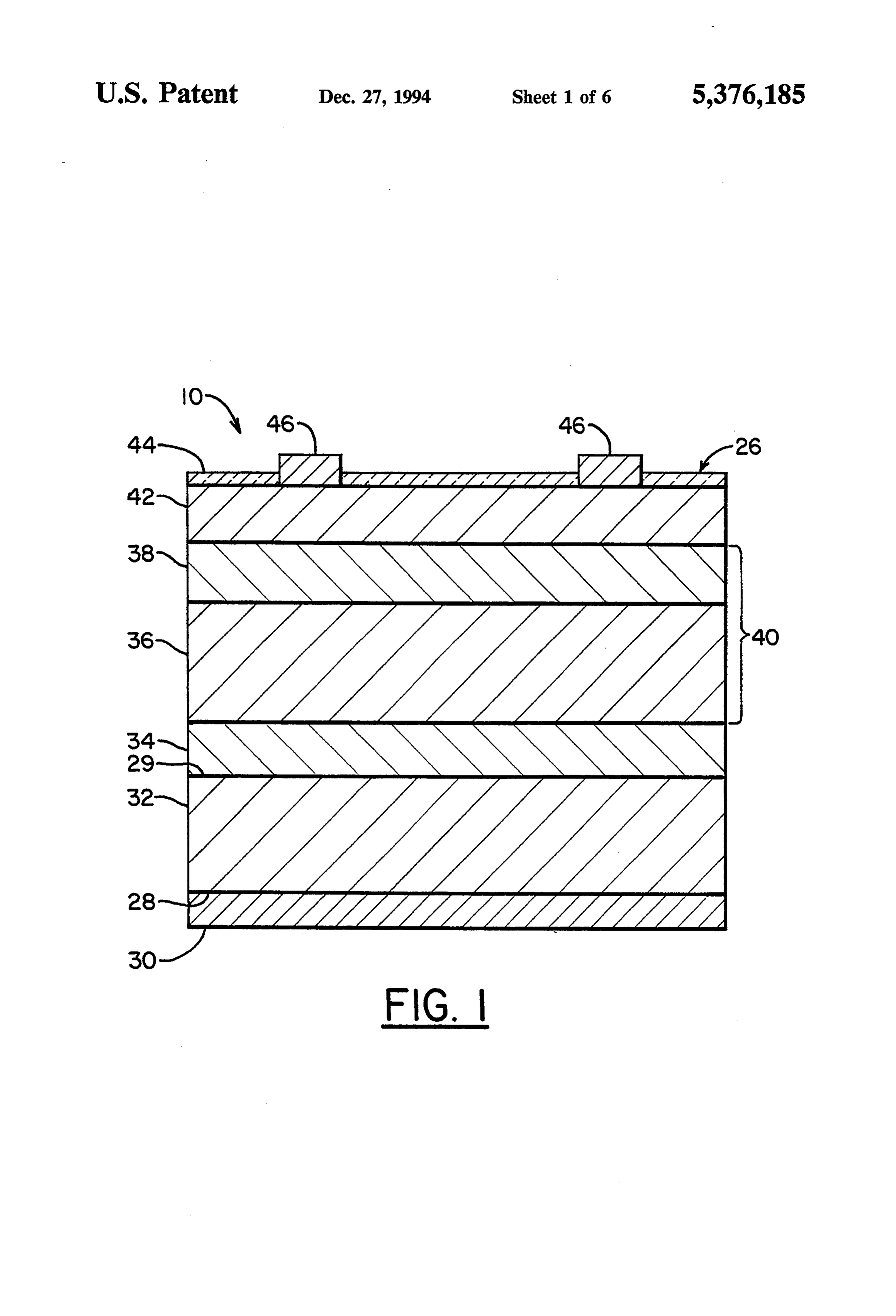
sisting of majority-carriers diffusing over the junction FIG. 1 is a cross-sectional view of the 1.14-0.02 eV barrier. This junction barrier is again related primarily 55 GanAsP concentrator solar cell of the present inven to the semiconductor intrinsic energy gap. tion;
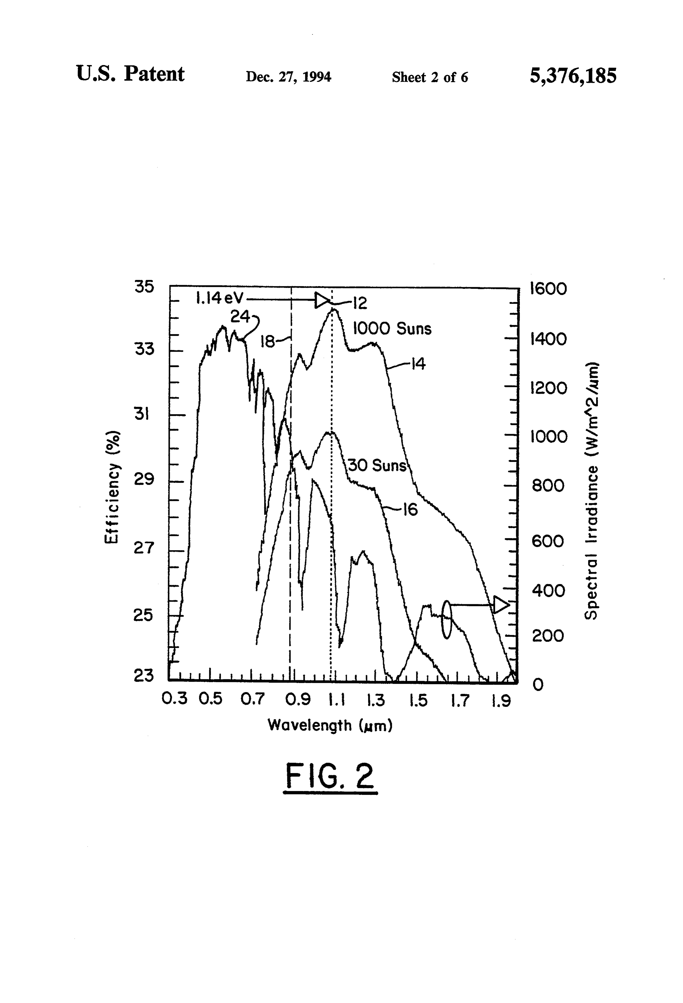
Doubling the light intensity incident on a solar cell in FIG. 2 is a plot of the spectral irradiance for the turn doubles the device short-circuit current. This in direct spectrum (ASTM E891) superimposed over a itself does not change the device energy-conversion graph of the modeled solar cell efficiency data as a efficiency. However, when the current in a diode is 60 function of energy gap (band gap) and concentration increased, the diode voltage increases. Since the solar ratio (C) for concentrations of 30 suns and 1000 suns at cell voltage increases with increasing light levels, the 25° C.;
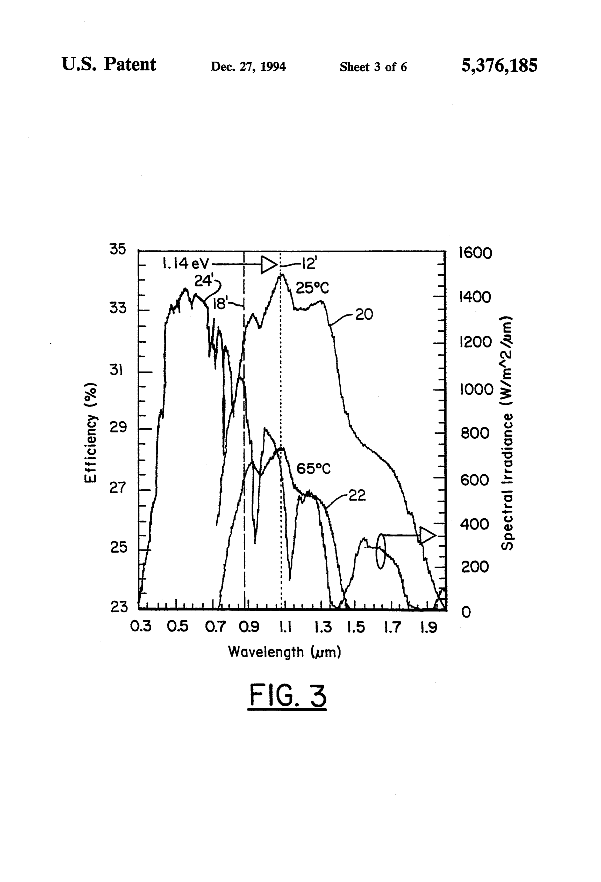
result is that the solar cell energy-conversion efficiency FIG. 3 is a plot of the spectral irradiance for the increases when operated with concentrated light. direct spectrum (ASTM E891) superimposed over a To date, the highest terrestrial efficiencies for single- 65 graph of the modeled solar cell efficiency data as a junction solar cells, approximately 28%, have been function of energy gap (band gap) and temperature for realized with GaAs homojunction devices at concentra temperatures at 25 C. and 65 C. at a fixed concentra tion ratios of approximately 200 suns. Close behind are tion of 1000 suns;
Page 9
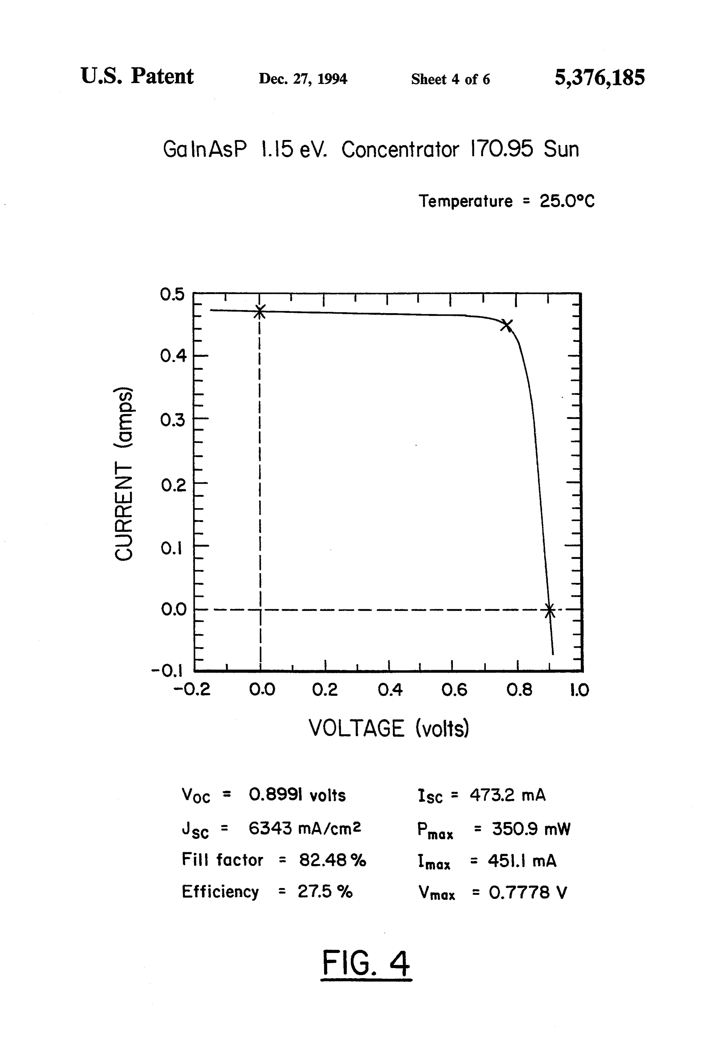
FIG. 4 is a graph of the current-voltage characteris advantage over the GaAs band gap 18 over a wide tics of the GanAsP concentrator cell of the present temperature range.
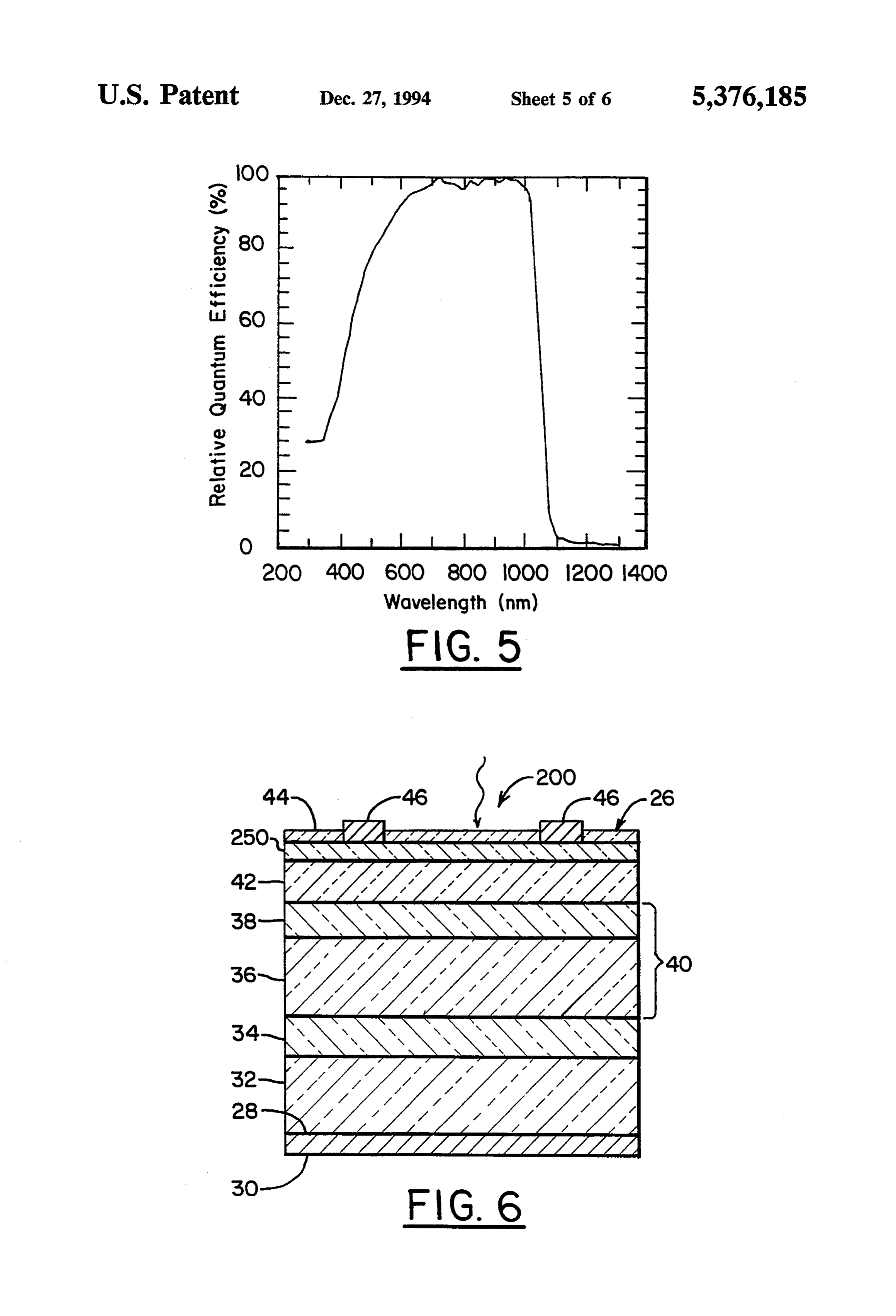
invention at peak performance; The data presented below in table 1 contains a sum FIG. 5 is a graph of the quantum efficiency data for mary of computer modeling results for single-junction the concentrator solar cell of the present invention, concentrator solar cells operated under the direct spec which displays a substantial drop in the blue response; trum (ASTM E891) as a function of the concentration FIG. 6 is a cross-sectional view of a first embodiment ratio, and at two temperatures. These data show that, of a GanAsP concentrator solar cell having a contact for high concentration ratios, the optimum band gap is ing layer interposed between the antireflective coating essentially independent of the concentration ratio and and the window layer; and 10
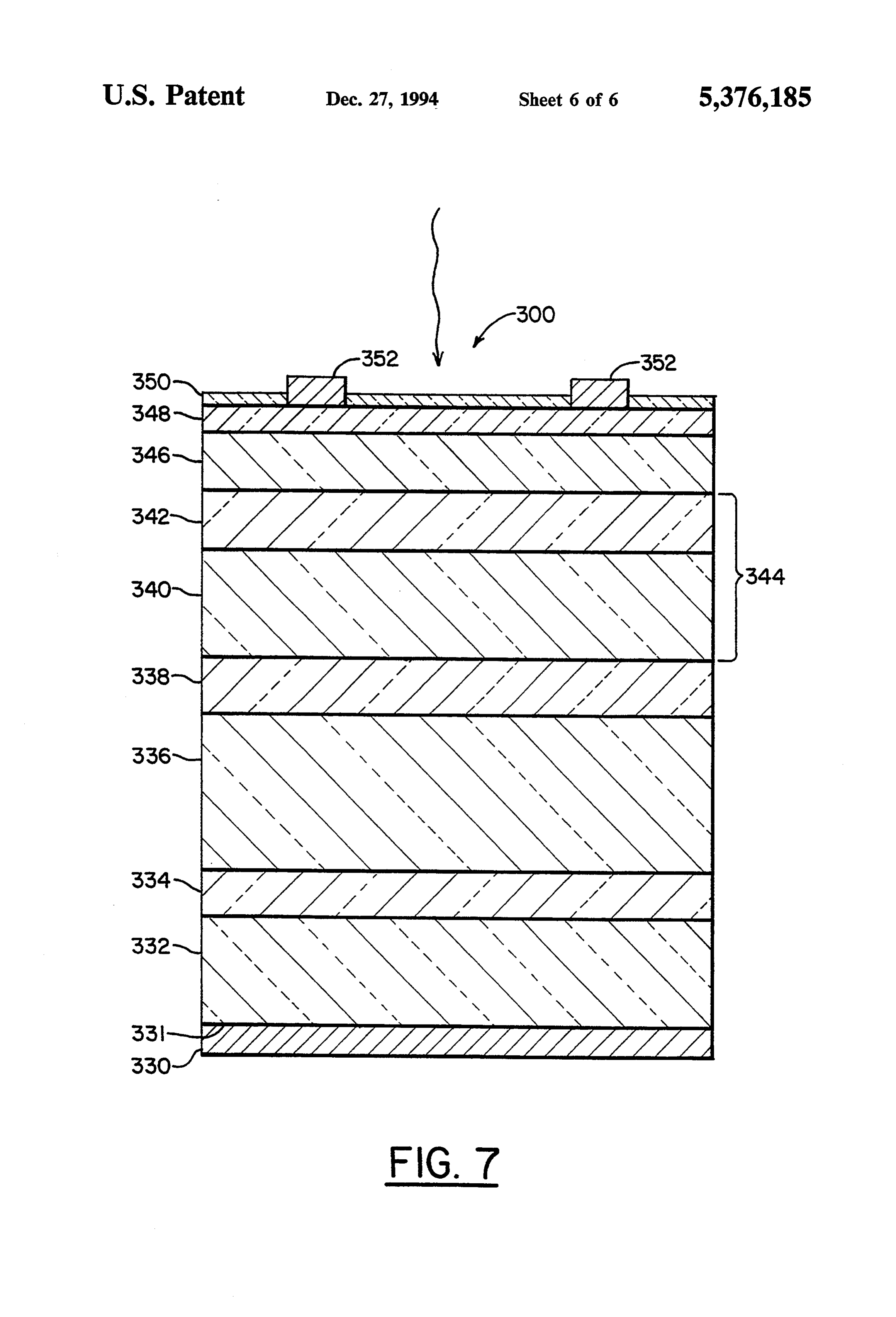
FIG. 7 is a cross-sectional view of a proposed second operating temperature and has a value of approximately embodiment of the present invention of a 1.140.02 eV band gap holds a these 1.14 eV. Second, data illustrate that the optimum significant efficiency advantage over
GanAs concentrator solar cell.
GaAs at high concentration ratios and at both tempera
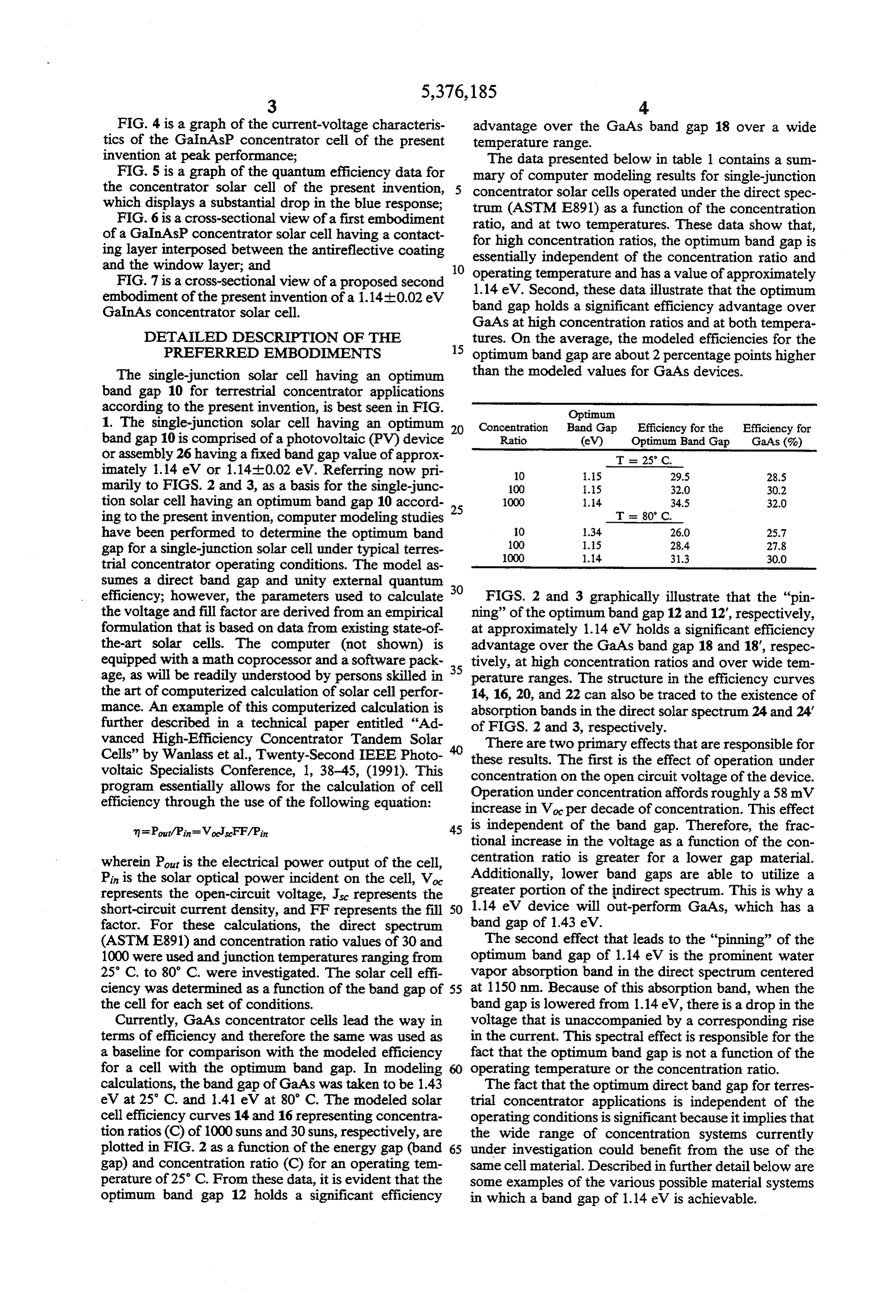
DETALED DESCRIPTION OF THE tures. On the average, the modeled efficiencies for the PREFERRED EMBODIMENTS 15 optimum band gap are about 2 percentage points higher The single-junction solar cell having an optimum than the modeled values for GaAs devices.
band gap 10 for terrestrial concentrator applications according to the present invention, is best seen in FIG. Optimum 1. The single-junction solar cell having an optimum 20 Concentration Band Gap Efficiency for the Efficiency for band gap 10 is comprised of a photovoltaic (PV) device Ratio (eV) Optimum Band Gap GaAs (%) or assembly 26 having a fixed band gap value of approx T - 25 C. imately 1.14 eV or 1.14-0.02 eV. Referring now pri 10 15 29.5 28.5 marily to FIGS. 2 and 3, as a basis for the single-junc 100 1.15 32.0 30.2 tion solar cell having an optimum band gap 10 accord 25 1000 1.4 34.5 32.0 ing to the present invention, computer modeling studies T = 80 C. have been performed to determine the optimum band 10 1.34 26.0 25.7 gap for a single-junction solar cell under typical terres 100
trial concentrator operating conditions. The model as sumes a direct band gap and unity external quantum 30 efficiency; however, the parameters used to calculate FIGS. 2 and 3 graphically illustrate that the "pin the voltage and fill factor are derived from an empirical ning' of the optimum band gap 12 and 12, respectively, formulation that is based on data from existing state-of at approximately 1.14 eV holds a significant efficiency the-art solar cells. The computer (not shown) is advantage over the GaAs band gap 18 and 18", respec equipped with a math coprocessor and a software pack 35 tively, at high concentration ratios and over wide tem age, as will be readily understood by persons skilled in perature ranges. The structure in the efficiency curves the art of computerized calculation of solar cell perfor 14, 16, 20, and 22 can also be traced to the existence of mance. An example of this computerized calculation is absorption bands in the direct solar spectrum 24 and 24 further described in a technical paper entitled "Ad of FIGS. 2 and 3, respectively.
vanced High-Efficiency Concentrator Tandem Solar There are two primary effects that are responsible for Cells” by Wanlass et al., Twenty-Second IEEE Photo these results. The first is the effect of operation under voltaic Specialists Conference, 1, 38-45, (1991). This program essentially allows for the calculation of cell concentration
Operation on the open circuit voltage of the device.
under concentration affords roughly a 58mV efficiency through the use of the following equation: increase in Voe per decade of concentration. This effect 45 is independent of the band gap. Therefore, the frac tional increase in the voltage as a function of the con wherein Pout is the electrical power output of the cell, centration ratio is greater for a lower gap material. Pin is the solar optical power incident on the cell, Voc Additionally, lower band gaps are able to utilize a represents the open-circuit voltage, Jsc represents the greater portion of the indirect spectrum. This is why a short-circuit current density, and FF represents the fill 50 1.14 eV device will out-perform GaAs, which has a factor. For these calculations, the direct spectrum band gap of 1.43 eV.
(ASTM E891) and concentration ratio values of 30 and The second effect that leads to the "pinning” of the 1000 were used and junction temperatures ranging from optimum band gap of 1.14 eV is the prominent water 25 C. to 80° C. were investigated. The solar cell effi vapor absorption band in the direct spectrum centered ciency was determined as a function of the band gap of 55 at 1150 nm. Because of this absorption band, when the the cell for each set of conditions. band gap is lowered from 1.14 eV, there is a drop in the Currently, GaAs concentrator cells lead the way in voltage that is unaccompanied by a corresponding rise terms of efficiency and therefore the same was used as in the current. This spectral effect is responsible for the a baseline for comparison with the modeled efficiency fact that the optimum band gap is not a function of the for a cell with the optimum band gap. In modeling operating temperature or the concentration ratio. calculations, the band gap of GaAs was taken to be 1.43 The fact that the optimum direct band gap for terres eV at 25 C. and 1.41 eV at 80 C. The modeled solar trial concentrator applications is independent of the cell efficiency curves 14 and 16 representing concentra operating conditions is significant because it implies that tion ratios (C) of 1000 suns and 30 suns, respectively, are the wide range of concentration systems currently plotted in FIG. 2 as a function of the energy gap (band 65 under investigation could benefit from the use of the gap) and concentration ratio (C) for an operating tem same cell material. Described in further detail below are perature of 25 C. From these data, it is evident that the some examples of the various possible material systems optimum band gap 12 holds a significant efficiency in which a band gap of 1.14 eV is achievable.
Page 10
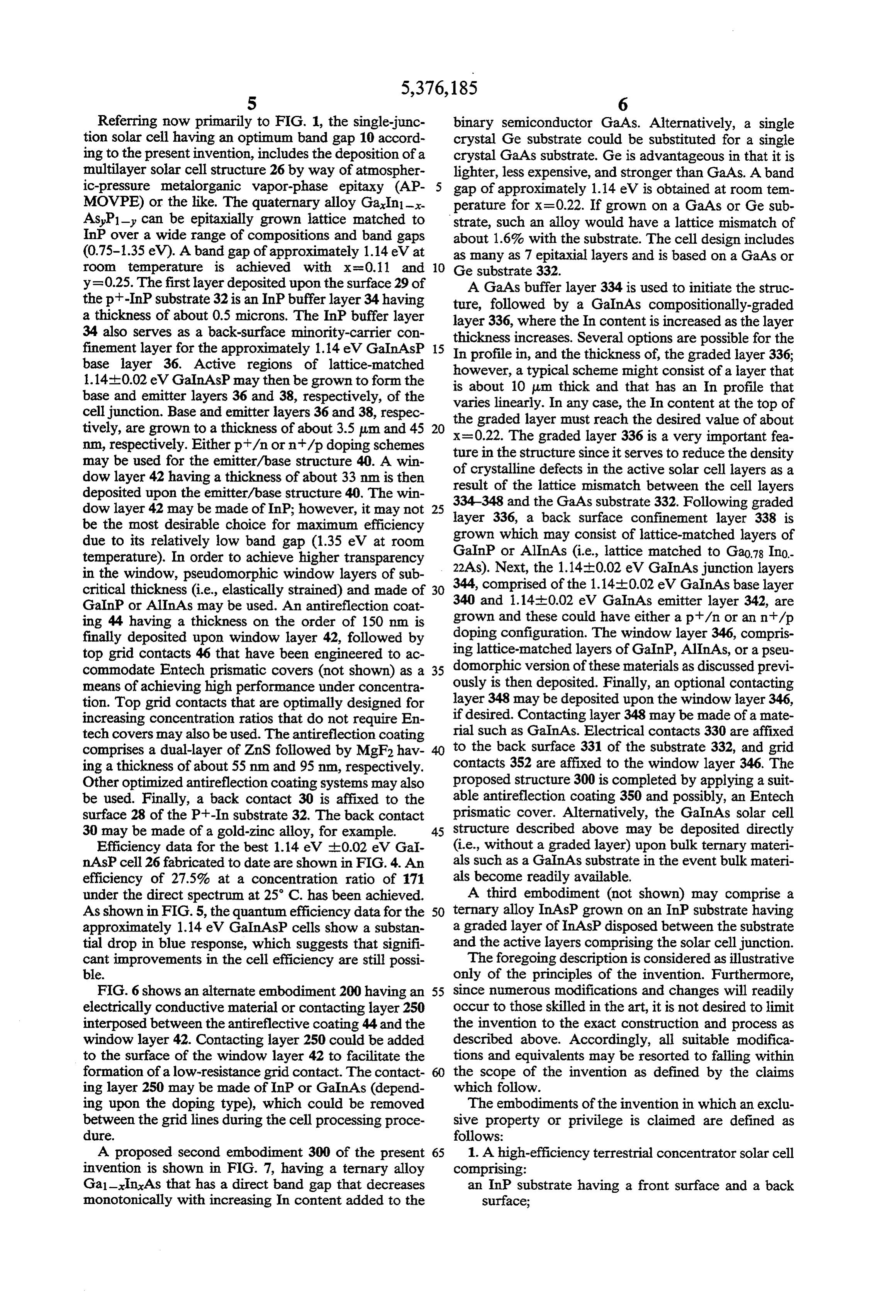
Referring now primarily to FIG. 1, the single-junc binary semiconductor GaAs. Alternatively, a single tion solar cell having an optimum band gap 10 accord crystal Ge substrate could be substituted for a single ing to the present invention, includes the deposition of a crystal GaAs substrate. Ge is advantageous in that it is multilayer solar cell structure 26 by way of atmospher lighter, less expensive, and stronger than GaAs. A band ic-pressure metalorganic vapor-phase epitaxy (AP gap of approximately 1.14 eV is obtained at room tem MOVPE) or the like. The quaternary alloy Gain-- perature for x=0.22. If grown on a GaAs or Ge sub AsP1-y can be epitaxially grown lattice matched to strate, such an alloy would have a lattice mismatch of InP over a wide range of compositions and band gaps about 1.6% with the substrate. The cell design includes (0.75-1.35 eV). A band gap of approximately 1.14 eV at as many as 7 epitaxial layers and is based on a GaAs or room temperature is achieved with x=0.11 and 10 Ge substrate 332.
y=0.25. The first layer deposited upon the surface 29 of A GaAs buffer layer 334 is used to initiate the struc the pt-InP substrate 32 is an InP buffer layer 34 having ture, followed by a GanAs compositionally-graded a thickness of about 0.5 microns. The InP buffer layer layer 336, where the In content is increased as the layer 34 also serves as a back-surface minority-carrier con thickness finement layer for the approximately 1.14 eV GanAsP 15 In profile increases.
in, and
Several options are possible for the the thickness of, the graded layer 336;
base layer 36. Active regions of lattice-matched however, a typical scheme 1.14-0.02 eV GainAsP may then be grown to form the is about 10 um thick and might that consist of a layer that has an In profile that base and emitter layers 36 and 38, respectively, of the varies linearly. In any case, the In content at the top of cell junction. Base and emitter layers 36 and 38, respec the graded layer must reach the desired value of about tively, are grown to a thickness of about 3.5 um and 45 20 x=0.22. The graded layer 336 is a very important fea nm, respectively. Either pt?/n or n/p doping schemes ture in the structure since it serves to reduce the density may be used for the emitter/base structure 40. A win dow layer 42 having a thickness of about 33 nm is then of crystalline defects in the active solar cell layers as a result of the lattice mismatch between the cell layers deposited upon the emitter/base structure 40. The win 334-348 and the GaAs substrate 332. Following graded dow layer 42 may be made of InP; however, it may not 25 layer 336, a back surface confinement layer 338 is be the most desirable choice for maximum efficiency grown which may consist of lattice-matched layers of due to its relatively low band gap (1.35 eV at room temperature). In order to achieve higher transparency Ganp or AlInAs (i.e., lattice matched to Gao.78 Ino in the window, pseudomorphic window layers of sub 344, 22As). Next, the 1.140.02 eV GanAs junction layers critical thickness (i.e., elastically strained) and made of 30 comprised of the 1.140.02 eV GanAs base layer Ganp or AlInAs may be used. An antireflection coat 340 and 1.14-0.02 eV GanAs emitter layer 342, are ing 44 having a thickness on the order of 150 nm is grown and these could have either a pan or an n/p finally deposited upon window layer 42, followed by doping configuration. The window layer 346, compris top grid contacts 46 that have been engineered to ac ing lattice-matched layers of GalnP, AlInAs, or a pseu commodate Entech prismatic covers (not shown) as a 35 domorphic version of these materials as discussed previ means of achieving high performance under concentra ously is then deposited. Finally, an optional contacting tion. Top grid contacts that are optimally designed for layer 348 may be deposited upon the window layer 346, increasing concentration ratios that do not require En ifrialdesired. Contacting layer 348 may be made of a mate such as GanAs. Electrical contacts 330 are affixed tech covers may also be used. The antireflection coating comprises a dual-layer of ZnS followed by MgF2 hav to the back surface 331 of the substrate 332, and grid ing a thickness of about 55 nm and 95 nm, respectively. contacts 352 are affixed to the window layer 346. The Other optimized antireflection coating systems may also proposed structure 300 is completed by applying a suit be used. Finally, a back contact 30 is affixed to the able antireflection coating 350 and possibly, an Entech surface 28 of the P-In substrate 32. The back contact prismatic cover. Alternatively, the GalnAs solar cell 30 may be made of a gold-zinc alloy, for example. 45 structure described above may be deposited directly Efficiency data for the best 1.14 eV -0.02 eV Gai (i.e., without a graded layer) upon bulk ternary materi nAsP cell 26 fabricated to date are shown in FIG. 4. An als such as a GanAs substrate in the event bulk materi efficiency of 27.5% at a concentration ratio of 171 als become readily available.
under the direct spectrum at 25 C. has been achieved. A third embodiment (not shown) may comprise a As shown in FIG. 5, the quantum efficiency data for the 50 ternary alloy InAsP grown on an InP substrate having approximately 1.14 eV GainAsP cells show a substan a graded layer of InAsP disposed between the substrate tial drop in blue response, which suggests that signifi and the active layers comprising the solar cell junction. cant improvements in the cell efficiency are still possi The foregoing description is considered as illustrative ble. only of the principles of the invention. Furthermore, FIG. 6 shows an alternate embodiment 200 having an 55 since numerous modifications and changes will readily electrically conductive material or contacting layer 250 occur to those skilled in the art, it is not desired to limit interposed between the antireflective coating 44 and the the invention to the exact construction and process as window layer 42. Contacting layer 250 could be added described above. Accordingly, all suitable modifica to the surface of the window layer 42 to facilitate the tions and equivalents may be resorted to falling within formation of a low-resistance grid contact. The contact the scope of the invention as defined by the claims ing layer 250 may be made of InP or GanAs (depend which follow.
ing upon the doping type), which could be removed The embodiments of the invention in which an exclu between the grid lines during the cell processing proce sive property or privilege is claimed are defined as dure. follows:
A proposed second embodiment 300 of the present 65 1. A high-efficiency terrestrial concentrator solar cell invention is shown in FIG. 7, having a ternary alloy comprising:
Ga1-x.inxAs that has a direct band gap that decreases an InP substrate having a front surface and a back monotonically with increasing In content added to the surface;
Page 11
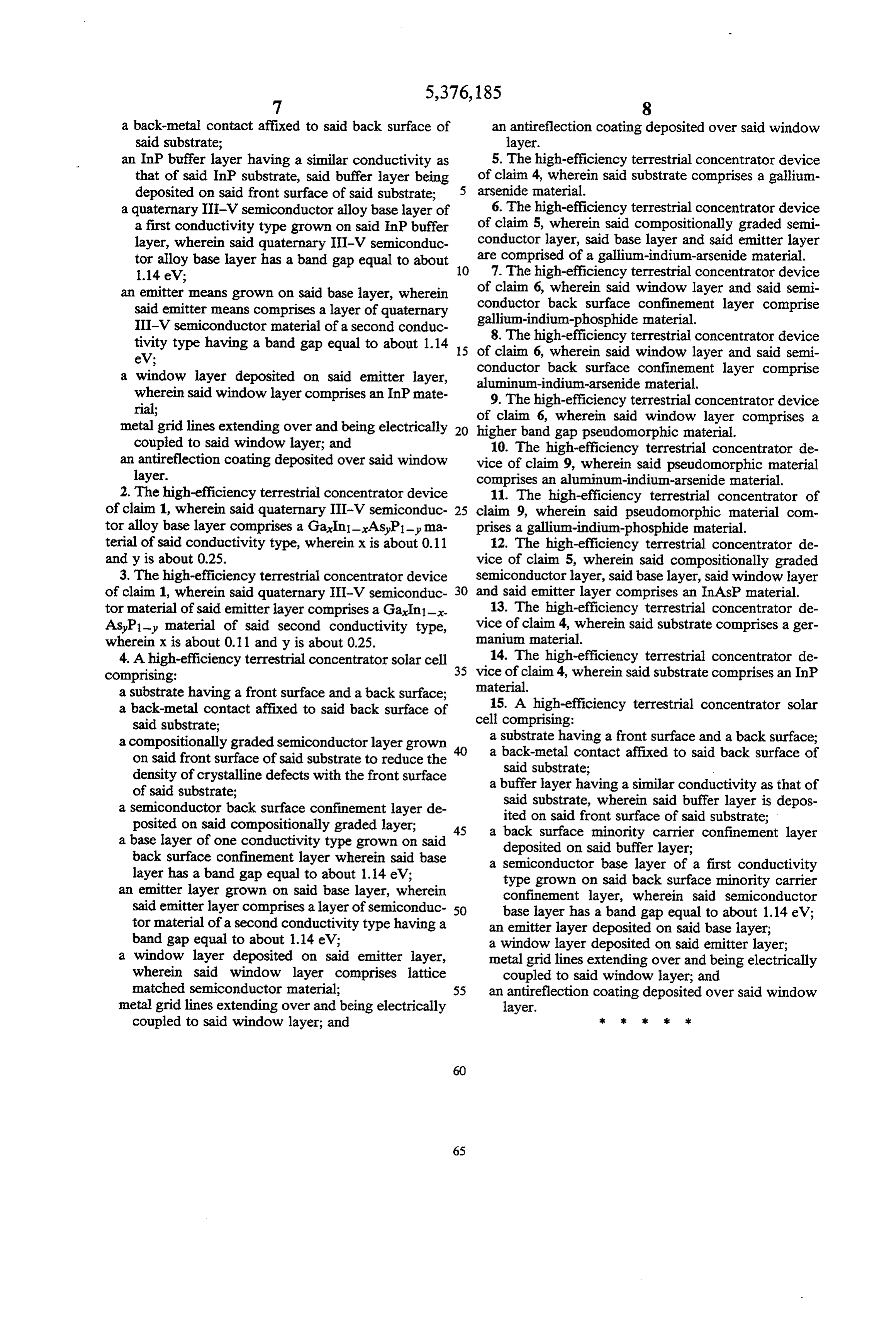
a back-metal contact affixed to said back surface of an antireflection coating deposited over said window said substrate; layer.
an InP buffer layer having a similar conductivity as 5. The high-efficiency terrestrial concentrator device that of said InP substrate, said buffer layer being of claim 4, wherein said substrate comprises a gallium deposited on said front surface of said substrate; 5 arsenide material.
a quaternary III-V semiconductor alloy base layer of 6. The high-efficiency terrestrial concentrator device a first conductivity type grown on said InP buffer of claim 5, wherein said compositionally graded semi layer, wherein said quaternary III-V semiconduc conductor layer, said base layer and said emitter layer tor alloy base layer has a band gap equal to about 10 are comprised of a gallium-indium-arsenide material. 1.14 eV; 7. The high-efficiency terrestrial concentrator device an emitter means grown on said base layer, wherein conductorof claim 6, wherein said window layer and said semi back surface confinement layer comprise said emitter means comprises a layer of quaternary gallium-indium-phosphide
III-V semiconductor material of a second conduc material. 8. The high-efficiency terrestrial tivity type having a band gap equal to about 1.14 15 of claim 6, wherein said window layer concentrator device eV; and said semi conductor back surface a window layer deposited on said emitter layer, aluminum-indium-arsenide material. confinement layer comprise wherein said window layer comprises an InP mate 9. The high-efficiency terrestrial concentrator device rial; of claim 6, wherein said window layer comprises a metal grid lines extending over and being electrically 20 higher band gap pseudomorphic material. coupled to said window layer; and 10. The high-efficiency terrestrial concentrator de an antireflection coating deposited over said window vice of claim 9, wherein said pseudomorphic material layer. comprises an aluminum-indium-arsenide material. 2. The high-efficiency terrestrial concentrator device 11. The high-efficiency terrestrial concentrator of of claim 1, wherein said quaternary III-V semiconduc 25 claim 9, wherein said pseudomorphic material com tor alloy base layer comprises a Gan1-xAsyP1-y ma prises a gallium-indium-phosphide material. terial of said conductivity type, wherein x is about 0.11 12. The high-efficiency terrestrial concentrator de and y is about 0.25. vice of claim 5, wherein said compositionally graded 3. The high-efficiency terrestrial concentrator device semiconductor layer, said base layer, said window layer of claim 1, wherein said quaternary III-V semiconduc 30 and said emitter layer comprises an InAsP material. tor material of said emitter layer comprises a Gan1-- 13. The high-efficiency terrestrial concentrator de AsP1-y material of said second conductivity type, vice of claim 4, wherein said substrate comprises a ger manium material.
wherein x is about 0.11 and y is about 0.25.
4. A high-efficiency terrestrial concentrator solar cell 35 14. The high-efficiency terrestrial concentrator de comprising: vice of claim 4, wherein said substrate comprises an InP a substrate having a front surface and a back surface; material.
a back-metal contact affixed to said back surface of 15. A high-efficiency terrestrial concentrator solar said substrate; cell comprising:
a compositionally graded semiconductor layer grown 40 aa substrate having a front surface and a back surface; back-metal contact affixed to said back surface of on said front surface of said substrate to reduce the density of crystalline defects with the front surface said substrate;
of said substrate; a buffer layer having a similar conductivity as that of a semiconductor back surface confinement layer de said substrate, wherein said buffer layer is depos posited on said compositionally graded layer; ited on said front surface of said substrate; a base layer of one conductivity type grown on said 45 a back surface minority carrier confinement layer back surface confinement layer wherein said base deposited on said buffer layer; layer has a band gap equal to about 1.14 eV; a semiconductor base layer of a first conductivity an emitter layer grown on said base layer, wherein type grown on said back surface minority carrier said emitter layer comprises a layer of semiconduc 50 confinement layer, wherein said semiconductor tor material of a second conductivity type having a base layer has a band gap equal to about 1.14 eV;
an emitter layer deposited on said base layer;
band gap equal to about 1.14 eV; a window layer deposited on said emitter layer; a window layer deposited on said emitter layer, metal grid lines extending over and being electrically wherein said window layer comprises lattice coupled to said window layer; and matched semiconductor material; 55 an antireflection coating deposited over said window metal grid lines extending over and being electrically layer.
coupled to said window layer; and k k xic : 2k
Page 12
UNITED STATES PATENT ANDTRADEMARK OFFICE
CERTFCATE OF CORRECTION
INVENTOR(S) : Mark W. Wanlass it is certified that error appears in the above-indentified patent and that said Letters Patent is hereby corrected as shown below:
In column 2, line 3, change "tinder" to -under-. Signed and Sealed this
Second Day of May, 1995
BRUCELEBMAN
Attesting Officer Commissioner of Patents and Trademarks
Provenance
- Collection
- Cited prior art
- Original PDF
- patentimages.storage.googleapis.com →
- Filed
- 1993-05-12
- Pages
- 12
- Method
- pdftotext (the PDF's own text layer) + pdftoppm 300dpi page scans
- Source
- Google Patents bibliographic record
- Granted
- 1994-12-27
- Inventors
- Mark W. Wanlass; Midwest Research Institute
- Transcribed from
- patentimages.storage.googleapis.com →