patent · US5136150
Image sensor having light guides for communication with image plane
4 August 1992
Page 1 — bibliographic record
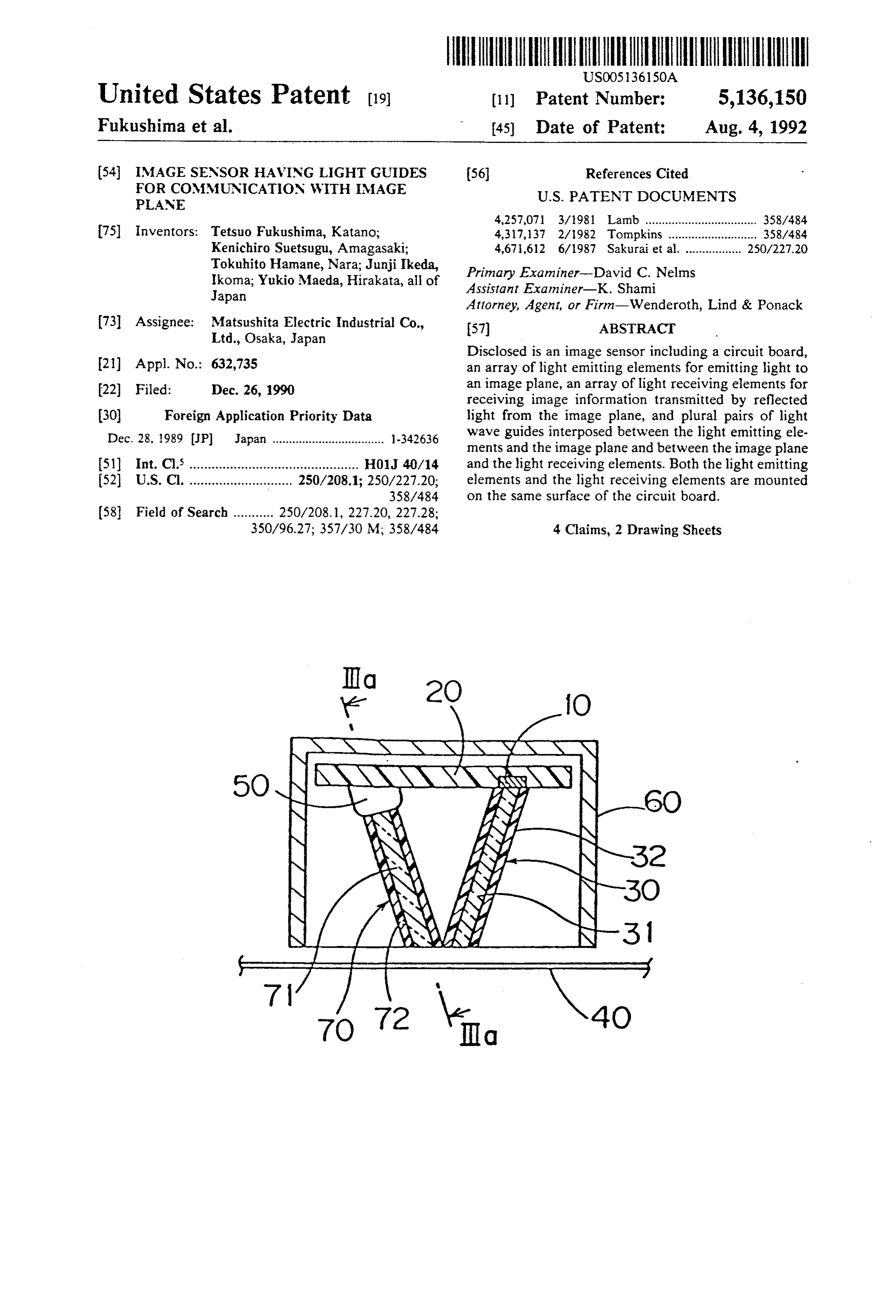
United States Patent (19) (1) Patent Number: 5,136,150 Fukushima et al. (45) Date of Patent: Aug. 4, 1992 (54) IMAGE SENSOR HAVING LIGHT GUIDES 56 References Cited FOR COMMUNICATION WITH IMAGE U.S. PATENT DOCUMENTS
PLANE A 4,257,071 3/1981 Lamb .................................. 358/.484 75 Inventors: Tetsuo Fukushima, Katano; 4,317,137 2/1982 Tompkins ........................... 358/.484 Kenichiro Suetsugu, Amagasaki; 4,67,612 6/1987 Sakurai et al. ................. 250/227.20 Tokuhito Hamane, Nara; Junji Ikeda, Primary Examiner-David C. Nelms
Ikoma; Yukio Maeda, Hirakata, all of Assistant Examiner-K. Shami
Japan
Attorney, Agent, or Firn-Wenderoth, Lind & Ponack 73 Assignee: Matsushita Electric Industrial Co., 57 ABSTRACT Ltd., Osaka, Japan
Disclosed is an image sensor including a circuit board, 21 Appl. No.: 632,735 an array of light emitting elements for emitting light to 22 Filed: Dec. 26, 1990 an image plane, an array of light receiving elements for receiving image information transmitted by reflected 30 Foreign Application Priority Data light from the image plane, and plural pairs of light Dec. 28, 1989 JP Japan .................................. -342636 wave guides interposed between the light emitting ele ments and the image plane and between the image plane 5) Int. Cl. .............................................. H01J 40/14 and the light receiving elements. Both the light emitting 52 U.S. Cl. ............................ 250/208.1; 250/227.20, elements and the light receiving elements are mounted 358/.484 on the same surface of the circuit board.
350/96.27; 357/30 M, 358/484 4. Claims, 2 Drawing Sheets
NRNNNNNSN
Page 2
Drawing sheet — no readable text.
Page 3
Drawing sheet — no readable text.
Page 4
In accomplishing this and other objects, an image
IMAGE SENSOR HAVING LIGHT GUIDES FOR sensor according to the present invention includes a CONNf UNICATION WITH IMAGE PLANE circuit board, at least one light emitting element for emitting light to an image plane, at least one light re
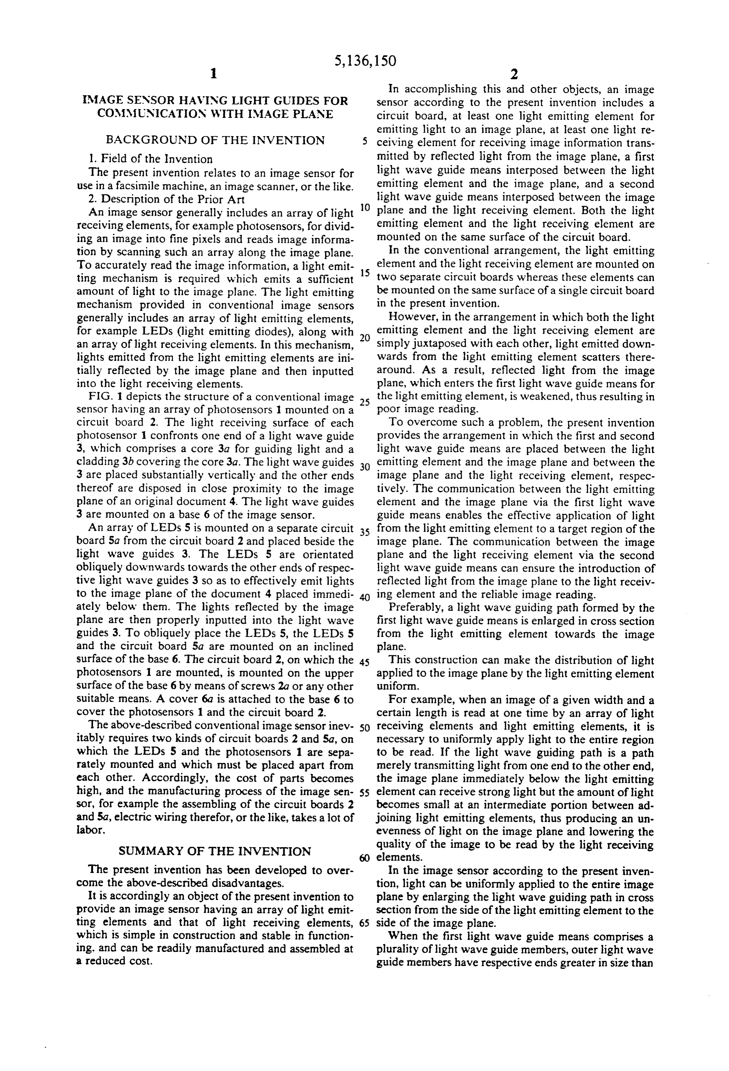
BACKGROUND OF THE INVENTION 5 ceiving element for receiving image information trans 1. Field of the Invention mitted by reflected light from the image plane, a first The present invention relates to an image sensor for light wave guide means interposed between the light use in a facsimile machine, an image scanner, or the like. emitting element and the image plane, and a second 2. Description of the Prior Art light wave guide means interposed between the image An image sensor generally includes an array of light O plane and the light receiving element. Both the light receiving elements, for example photosensors, for divid emitting element and the light receiving element are ing an image into fine pixels and reads image informa mounted on the same surface of the circuit board. tion by scanning such an array along the image plane. In the conventional arrangement, the light emitting To accurately read the image information, a light emit 15 element and the light receiving element are mounted on ting mechanism is required which emits a sufficient two separate circuit boards whereas these elements can amount of light to the image plane. The light emitting be mounted on the same surface of a single circuit board mechanism provided in conventional image sensors in the present invention.
generally includes an array of light emitting elements, However, in the arrangement in which both the light for example LEDs (light emitting diodes), along with 20 emitting element and the light receiving element are an array of light receiving elements. In this mechanism, simply juxtaposed with each other, light emitted down lights emitted from the light emitting elements are ini wards from the light emitting element scatters there tially reflected by the image plane and then inputted around. As a result, reflected light from the image into the light receiving elements. plane, which enters the first light wave guide means for FIG. 1 depicts the structure of a conventional image 25 the light emitting element, is weakened, thus resulting in sensor having an array of photosensors 1 mounted on a poor image reading.
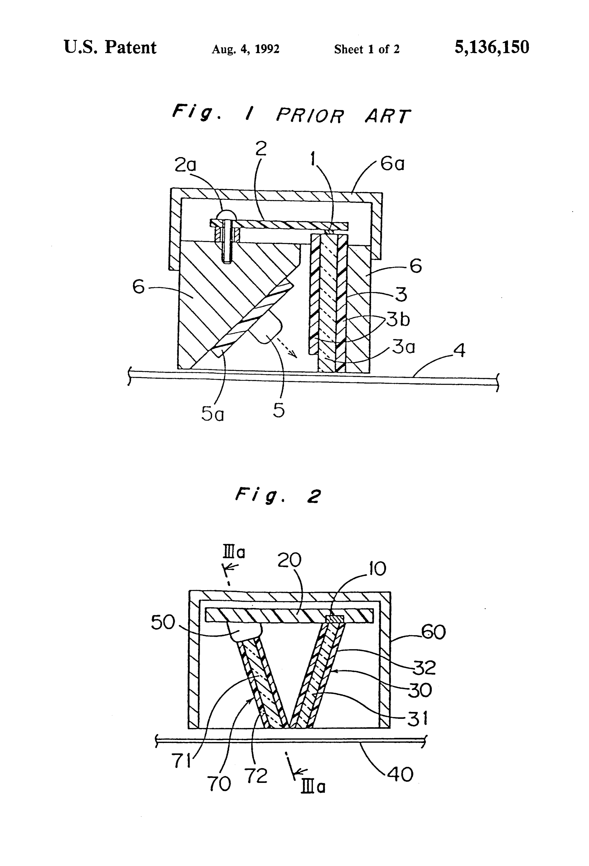
circuit board 2. The light receiving surface of each To overcome such a problem, the present invention photosensor confronts one end of a light wave guide provides the arrangement in which the first and second 3, which comprises a core 3a for guiding light and a light wave guide means are placed between the light cladding 3b covering the core 3a. The light wave guides 30 emitting element and the image plane and between the 3 are placed substantially vertically and the other ends image plane and the light receiving element, respec thereof are disposed in close proximity to the image tively. The communication between the light emitting plane of an original document 4. The light wave guides element and the image plane via the first light wave 3 are mounted on a base 6 of the image sensor. guide means enables the effective application of light An array of LEDs 5 is mounted on a separate circuit 35 from the light emitting element to a target region of the board 5a from the circuit board 2 and placed beside the image plane. The communication between the image light wave guides 3. The LEDs 5 are orientated plane and the light receiving element via the second obliquely downwards towards the other ends of respec light wave guide means can ensure the introduction of tive light wave guides 3 so as to effectively emit lights reflected light from the image plane to the light receiv to the image plane of the document 4 placed immedi ing element and the reliable image reading. ately below them. The lights reflected by the image Preferably, a light wave guiding path formed by the plane are then properly inputted into the light wave first light wave guide means is enlarged in cross section guides 3. To obliquely place the LEDs 5, the LEDs 5 from the light emitting element towards the image and the circuit board 5a are mounted on an inclined plane.
surface of the base 6. The circuit board 2, on which the 45 This construction can make the distribution of light photosensors 1 are mounted, is mounted on the upper applied to the image plane by the light emitting element surface of the base 6 by means of screws 2a or any other uniforn.
suitable means. A cover 6a is attached to the base 6 to For example, when an image of a given width and a cover the photosensors 1 and the circuit board 2. certain length is read at one time by an array of light The above-described conventional image sensor inev 50 receiving elements and light emitting elements, it is itably requires two kinds of circuit boards 2 and 5a, on necessary to uniformly apply light to the entire region which the LEDs 5 and the photosensors 1 are sepa to be read. If the light wave guiding path is a path rately mounted and which must be placed apart from merely transmitting light from one end to the other end, each other. Accordingly, the cost of parts becomes the image plane immediately below the light emitting high, and the manufacturing process of the image sen 55 element can receive strong light but the amount of light sor, for example the assembling of the circuit boards 2 becomes small at an intermediate portion between ad and 5a, electric wiring therefor, or the like, takes a lot of joining light emitting elements, thus producing an un labor. evenness of light on the image plane and lowering the SUMMARY OF THE INVENTION quality of the image to be read by the light receiving elements.
The present invention has been developed to over In the image sensor according to the present inven come the above-described disadvantages. tion, light can be uniformly applied to the entire image It is accordingly an object of the present invention to plane by enlarging the light wave guiding path in cross provide an image sensor having an array of light emit section from the side of the light emitting element to the ting elements and that of light receiving elements, 65 side of the image plane.
which is simple in construction and stable in function When the first light wave guide means comprises a ing. and can be readily manufactured and assembled at plurality of light wave guide members, outer light wave a reduced cost. guide members have respective ends greater in size than
Page 5
those of inner light wave guide members so that highly between the core 31 and the cladding 32 and is transmit uniform light may be applied to the entire image plane. ted to the other end of the core 31. Poly-carbonate, Furthermore, the brightness of the entire image plane epoxy resin, acrylic resin, glass, or the like can be used can be made uniform even when the distance between as the material of the core 31 or that of the cladding 32. the light emitting elements is extended. Accordingly, The index of refraction can be made different by regu the number of the light emitting elements required for lating the composition or the compounding ingredient reading an image of a given width can be reduced. of resin or glass. A light absorbing material or a light BRIEF DESCRIPTION OF THE DRAWINGS dispersing material may be mixed into the cladding 32. The light wave guide 30 made of the above-described
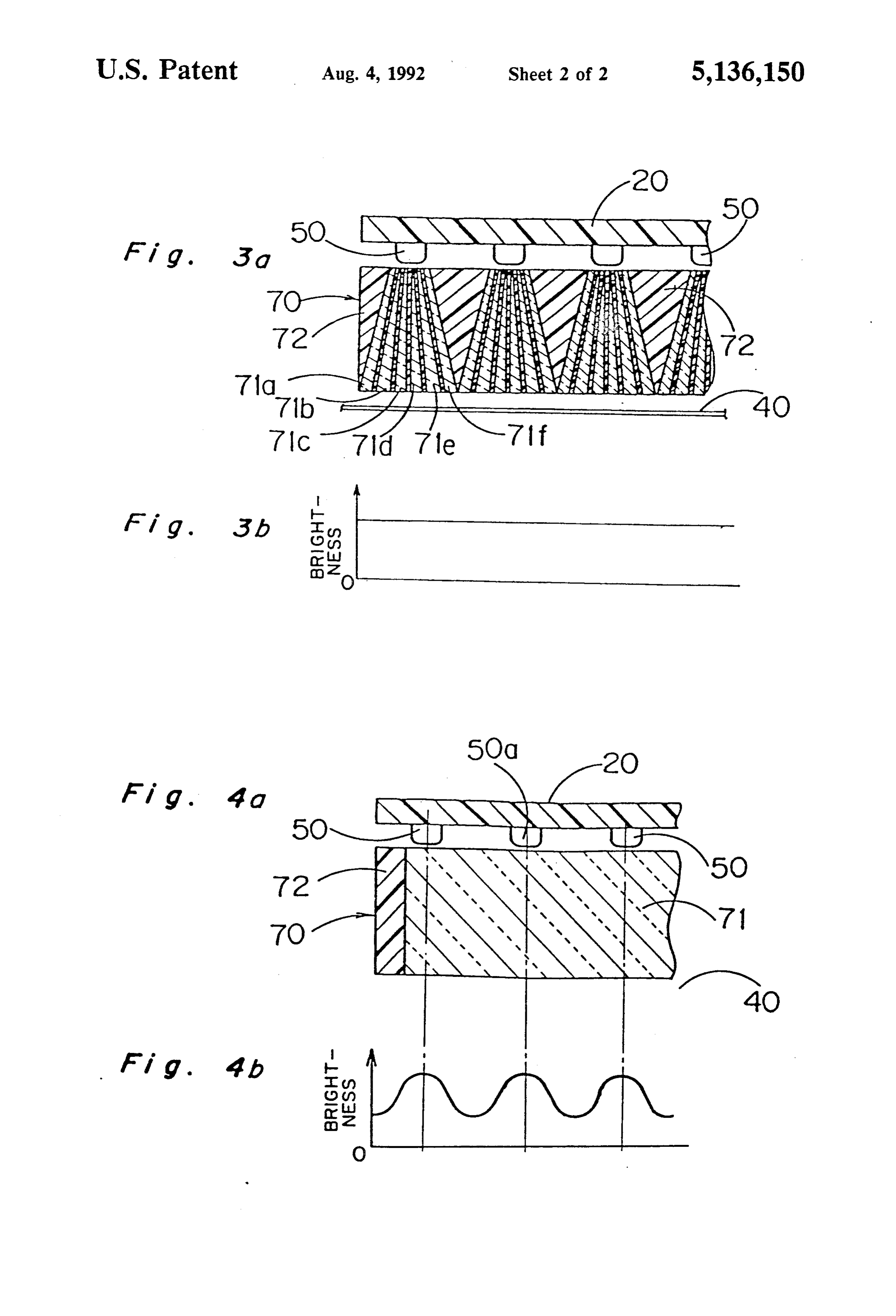
This and other objects and features of the present 10 material is manufactured using a molding technique or a invention will become more apparent from the follow thin film processing technique for resin or glass, as simi ing description of a preferred embodiment thereof with lar to the ordinary light wave guides. reference to the accompanying drawings, throughout In the illustrated embodiment, the light wave guide which like parts are designated by like reference numer 30 extends slightly obliquely downwards from the als, and wherein: 15 lower surface of the circuit board 20, as viewed in FIG. FIG. 1 is a schematic cross-sectional view of a con 2. It is to be noted that in the embodiment, although the ventional image sensor; light wave guide 30 is securely mounted on the surface FIG. 2 is a schematic cross-sectional view of an of the circuit board 20, it may be carried by a support image sensor according to the present invention; member or a base (not shown) of resin or the like. FIG.3a is a schematic sectional view taken along line 20 The light emitting element 50 is mounted on the IIIa-IIIa in FIG. 2; lower surface of the circuit board 20 so as to emit light FIG. 3b is a graph indicative of the brightness of an obliquely downwards, as viewed in FIG. 2. A light image plane in the construction of FIG. 3a; wave guide 70 extends from the lower surface of each FIG. 4a is a schematic sectional view of an image light emitting element 50 in a direction of travel of the sensor having a construction different from the image 25 light emitted from the light emitting element 50. The sensor of FIG. 2; and lower end of the light wave guide 70 is placed in close FIG. 4b is a graph indicative of the brightness of an proximity to the image plane and the lower end of the image plane in the construction of FIG. 4b. light wave guide 30 for the corresponding light receiv DETAILED DESCRIPTION OF THE ing element 10. As a result, each pair of the light wave 30 guides 30 for the light receiving elements 10 and the
PREFERRED EMBODIMENT
light wave guides 70 for the light emitting elements 50
Referring now to the drawings, there is shown in is substantially in the form of a figure "V". FIG. 2 an image sensor according to the present inven As shown in FIG. 3a, each of the light wave guides tion, which includes a circuit board 20, an array of light 70 for the light emitting elements 50 has a plurality of receiving elements 10 such as photosensors, and an 35 light wave guiding paths constituted by a plurality of array of light emitting elements 50 such as LEDs. Both core members 71a-71f and aligned in a direction of the light receiving elements 10 and the light emitting array of the light emitting elements 50. The core mem elements 50 are securely mounted on the circuit board bers 71a-71f have respective lower ends having the 20 and spaced a certain distance from each other. The same sectional area on the side of the original document array of the light receiving elements 10 and that of the and taper linearly towards the light emitting element 50 light emitting elements 50 extend in parallel with each to the extent of being substantially the same as the width other in a direction perpendicular to the plane of FIG. of the light emitting element 50. The upper ends of the 2. The light receiving surface of each light receiving outer two core members 71a and 71 f have the same element 10 confronts one end of a light wave guide 30, sectional area greater than those of any other core mem the other end of which is placed in close proximity to an 45 bers 71b-71e whereas the upper ends of the inner two image plane of an original document 40. The light wave core members 71c and 71d have the smallest sectional guide 30 comprises a core 31, interposed between the area so that substantially uniform lights may be applied light receiving surface of the light receiving element 10 to the original document through the core members and the image plane, for guiding light and a cladding 32 71a-71f covering the core 31. Image information from the image 50 FIG. 3b is a graph indicative of the distribution of plane is inputted into the light receiving element 10 brightness on the original document. It is known from through the core 31. this graph that the entire image plane is uniform in Any other suitable electronic elements as employed brightness and a sufficient brightness is present even at in the conventional image sensors or any other known a location between the light emitting elements 50. electronic appliances can be used, as well as the above 55 The above-described light wave guide 70 is com described LEDs or photosensors, as the light receiving pared hereinafter with a conventionally known light elements 10 or the light emitting elements 50. wave guide in the form of a sheet. Any other suitable members having a construction FIG. 4a shows the state in which a light wave guide and made of a material as similar to those employed in having a conventional construction is used as the light various optical devices to constitute a light wave guid wave guide 70 for the light emitting elements 50. This ing path can be used as the light wave guide 30. For light wave guide 70 has a core 71 in the form of a sheet example, the light wave guide 30 is constituted by a and a cladding 72 formed so as to encircle the periphery plurality of rod-like core members made of a transpar thereof.
ent material such as glass, a macromolecular material, FIG. 4b is a graph similar to FIG. 3b in the case or the like and having a large index of refraction and a 65 where such a light wave guide 70 is used. It is known cladding having a small index of refraction and encir from this graph that although a sufficient brightness is cling all the core members. Light entering one end of present at the locations below the light emitting ele the core 31 is entirely reflected at a boundary surface ments 50 and 50a, the amount of light is relatively small
Page 6
at the location below an intermediate portion between and between the image plane and the light receiving the adjoining light emitting elements 50 and 50a and the elements can ensure the accurate and effective applica brightness is uneven in the longitudinal direction of the tion of light from the light emitting elements to a target original document. location on the image plane, thereby considerably in Accordingly, as shown in FIGS. 3a and 3b, the proving the image quality.
brightness on the image plane can be uniform by enlarg In addition, even if the distance between the light ing the core 71, which constitutes a light wave guiding emitting elements is extended, the image quality is path, from the side of the light emitting element 50 hardly lowered in the arrangement according to the towards the side of the original document and by present invention, and therefore, the number of the light changing the sectional area of the core members O emitting elements can be reduced as compared with the 71a-71 fon the side of the original document. As a re sult, the quality of an image to be read can be improved. conventional emitting image sensor. Because of this, the light elements and the circuit board, on which the
It is to be noted that the light wave guide 70 having the light emitting elements are mounted, can be simplified construction of FIG. 4a is also usable according to the in construction and the manufacturing cost thereof can object or use thereof. It is also to be noted that although 15 be reduced.
six core members 71a-71f form one light emitting ele Although the present invention has been fully de ment 50 in FIG. 3a, the number thereof may be in scribed by way of examples with reference to the ac creased or decreased according to the object or use companying drawings, it is to be noted here that various thereof.
In applications where the light wave guide 70 shown skilled in the modifications 20 changes and art. Therefore, will be apparent to those unless such changes and in FIG. 3a is employed, the distance between adjoining modifications otherwise depart light emitting elements 50 can be widened so that the scope of the present invention, theyfrom the spirit and should be construed number of the light emitting elements 50 may be re duced. For example, light can be applied to the entire as What being included therein.
image plane using a single light emitting element 50. 25 1. An isimage claimed is:
sensor comprising:
In the image sensor according to the present inven a circuit board;
tion, light emitted from the light emitting element 50 is directed obliquely downwards to the image plane at least one light emitting element, mounted on one through the light wave guide 70, and the light reflected surface of said circuit board, for emitting light to an by the image plane is directed obliquely upwards to the 30 image plane;
light receiving element 10 through the light wave guide at least one light receiving element, mounted on said 30 so that the image may be read. surface of said circuit board, for receiving image Preferably, the lower end of the core 31 of the light information transmitted by reflected light form the wave guide 30 may be partially uncovered by cutting image plane;
out a portion of the cladding 32 or the lower end of the 35 a first light wave guide means interposed between core 31 may be obliquely cut out, thereby facilitating said light emitting element and said image plane; the introduction of light into the light wave guide 30. and
Furthermore, the provision of a semicircular lens at a a second light wave guide means interposed between location close to the lower end of the light wave guide said light receiving element and a position at said 30 or 70 can converge or deflect light to be applied to image plane where it will pick up light form said the original document or light reflected by the original first light wave guide means which is reflected at document so that the application of light or the image the image plane, said first light wave guide means reading may be effectively performed. The lower ends having a light wave guiding path which is enlarged of the light wave guides 30 and 70 may be coated with in cross section from said light emitting element a hard coating material or covered with respective thin 45 towards said image plane. protective glass layers. In this case, the lower ends of 2. The image sensor according to claim 1, wherein the light wave guides 30 and 70 are never worn out said first light wave guide means comprises a plurality even if they are brought into contact with the original of light wave guide members positioned in a line and document. wherein the light wave guide members at the ends of The image sensor according to the present invention 50 the line have respective ends greater in size than those is applicable to a facsimile machine, an image scanner, a of the light wave guide members in the middle of the copier or any other apparatus in which an image is line.
electronically treated. 3. The image sensor according to claim 1, wherein According to the present invention, the number of said first light wave guide means and said second light the circuit boards can be reduced because both the light 55 wave guide means are inclined in opposite directions emitting elements and the light receiving elements are with respect to said image plane.
mounted on the same surface of the circuit board, thus 4. The image sensor according to claim 1, wherein remarkably reducing the cost of parts and the assem said first and second light wave guide means are posi bling cost. tioned substantially in the form of a figure "V" with the Furthermore, the provision of the light wave guides 60 apex adjacent the image plane.
between the light emitting elements and the image plane 8
Provenance
- Collection
- Cited prior art
- Original PDF
- patentimages.storage.googleapis.com →
- Filed
- 1990-12-26
- Pages
- 6
- Method
- pdftotext (the PDF's own text layer) + pdftoppm 300dpi page scans
- Source
- Google Patents bibliographic record
- Granted
- 1992-08-04
- Inventors
- Tetsuo Fukushima; Kenichiro Suetsugu; Tokuhito Hamane; Junji Ikeda; Yukio Maeda; Matsushita Electric Industrial Co Ltd
- Transcribed from
- patentimages.storage.googleapis.com →