patent · US4767172
Collector for an LED array
30 August 1988
Page 1 — bibliographic record
United States Patent (19) 11 Patent Number: 4,767,172 Nichols et al. (45) Date of Patent: Aug. 30, 1988 (54) COLLECTOR FOR AN LED ARRAY 4,255,042 3/1981 Armitage et al. .................. 355/3 R 4,257,672 3/1981 Balliet .............................. 350/96.17 (75) Inventors: Virginia R. Nichols, Spencerport; Primary Examiner-Fred L. Braun Fred F. Hubble, III, Rochester;
James P. Martin, Dansville, all of Attorney, Agent, or Firm-Ronald F. Chapuran
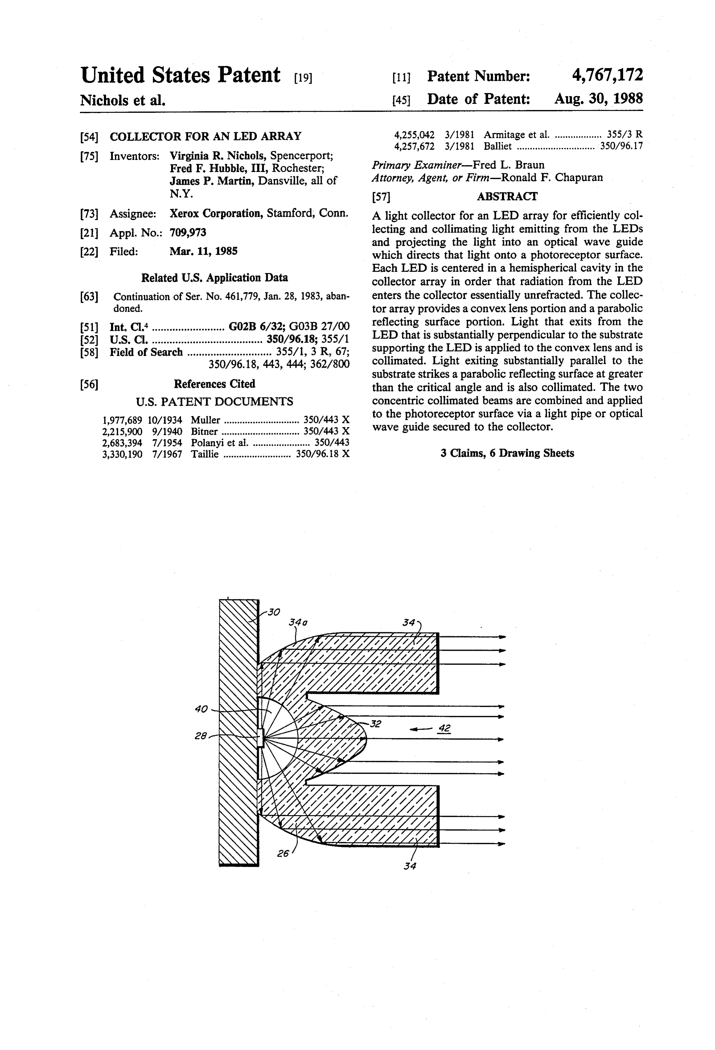
N.Y. 57 ABSTRACT (73) Assignee: Xerox Corporation, Stamford, Conn. A light collector for an LED array for efficiently col (21) Appl. No.: 709,973 lecting and collimating light emitting from the LEDs and projecting the light into an optical wave guide 22 Filed: Mar. 11, 1985 which directs that light onto a photoreceptor surface. Each LED is centered in a hemispherical cavity in the
Related U.S. Application Data collector array in order that radiation from the LED (63) Continuation of Ser. No. 461,779, Jan. 28, 1983, aban enters the collector essentially unrefracted. The collec doned. tor array provides a convex lens portion and a parabolic (51) Int. Cl."......................... G02B 6/32; G03B 27/00 reflecting surface portion. Light that exits from the (52) U.S. C. ...................................... 350/96.18; 355/1 LED that is substantially perpendicular to the substrate (58) Field of Search ............................. 355/1, 3 R, 67; supporting the LED is applied to the convex lens and is 350/96.18, 443, 444; 362/800 collimated. Light exiting substantially parallel to the substrate strikes a parabolic reflecting surface at greater (56) References Cited than the critical angle and is also collimated. The two
1,977,689 10/1934 Muller ... ... 350/443 X to the photoreceptor surface via a light pipe or optical 2,215,900 9/1940 Bitner ........... ... 350/443 X wave guide secured to the collector. 2,683,394 7/1954 Polanyi et al. ...................... 350/443 3,330, 190 7/1967 Taillie .......................... 350/96.18 X 3 Claims, 6 Drawing Sheets
Page 2
Drawing sheet — no readable text.
Page 3
Drawing sheet — no readable text.
Page 4
Drawing sheet — no readable text.
Page 5
Drawing sheet — no readable text.
Page 6
Drawing sheet — no readable text.
Page 7
Drawing sheet — no readable text.
Page 8
addition, it is relatively complex and expensive to
COLLECTOR FOR AN LED ARRAY mount and package a large array of discrete LEDs. It would be desirable, therefore, to provide an efficient
This is a continuation, of application Ser. No. and simple means to collect and propagate light in a 461,779, filed Jan. 28, 1983, now abandoned. 5 well controlled manner from an array of LEDs to a The present invention relates to a light collector for photoconductive surface.
an LED array, in particular a light collector for an It is, therefore, an object of the present invention to array used in an electrophotographic machine for patch provide a new and improved light collector for an LED generation on a photoreceptor surface and for pitch and array. It is another object of the present invention to edge erasure on the surface. 10 provide a light collector for an LED array for use in Light emitting diodes (LEDs) are low cost, reliable discharging selected portions of a photoconductive light sources that emit light patterns that are generally surface.
broad. The broad light patterns of LEDs often impede It is still another object of the present invention to the efficient of the LEDs with light pipes, optical wave provide a light collector for an LED light source that guides or other optical transmission media. 15 forms a hemispherical cavity about an LED and pro It is known to optically couple an LED to a light pipe vides both a convex lens and a parabolic reflecting by abutting the end of the light pipe against the LED. surface for collecting and directing light emitted from Since the LED source is small, however, proper align the LED.
ment is difficult. Furthermore, when the acceptance It is another object of the present invention to pro angle of the light pipe is small, coupling is inefficient. vide a means to collect radiation emitted from the sides Lenses and reflectors have been used to focus and of an LED into a collimated beam of light. collimate a wide emission LED. However, with the use Further objects and advantages of the present inven of lenses and reflectors alignment is often difficult and tion will become apparent as the following description therefore expensive. For example, as disclosed in U.S. proceeds and the features of novelty characterizing the Pat. No. 4,257,672, a spherical lens structure is used as 25 invention will be pointed out with particularity in the an optical coupler for coupling a relatively wide emis claims annexed to and forming a part of this specifica sion light source to an optical transmission line. In par tion.
ticular, the wide emission light source is mounted adja Briefly, the present invention is a light collector for cent the center of one end of a cylinder. The spherical an LED array for efficiently collecting and collimating lens structure is mounted on the opposite end of the 30 light emitting from the LEDs and projecting the light cylinder at a predetermined distance from the light into an optical wave guide which directs that light onto source and in an orientation to maximize the amount of a photoreceptor surface. Each LED is centered in a light entering the optical transmission line. A difficulty hemispherical cavity in the collector array in order that with this type of construciton, particularly in using an radiation from the LED enters the collector essentially array of LEDs, is the need to align each discrete LED 35 unrefracted. The collector array provides a convex lens with a spherical structure. In addition, only light strik portion and a parabolic reflecting surface portion. Light ing the spherical surface is captured in the light pipe. It that exits from the LED that is substantially perpendic would be desirable, therefore, to provide a relatively ular to the substrate supporting the LED is applied to inexpensive, reliable and simple means to optimize the the convex lens and is collimated. Light exiting substan collection of light from an array of LEDs at one end of 40 tially parallel to the substrate strikes a parabolic reflect a light pipe. ing surface at greater than the critical angle and is also Other prior art references such as U.S. Pat. No. collimated. The two concentric collimated beams are 4,255,042, teach the use of an LED array as an erase combined and applied to the photoreceptor surface via lamp to discharge portions of a photoconductive sur a light pipe or optical wave guide secured to the collec face. Conventionally, in electrophotographic machines, 45 tor.
erase lamps have been incandescent or fluorescent Other objects and advantages of the present invention lamps in which the lamp illumination has been attenu will become apparent upon reading the following de ated by shields to the photoconductor to obtain sharp tailed description and upon reference to the drawings in edge delineation of the erased charge on the photocon which:
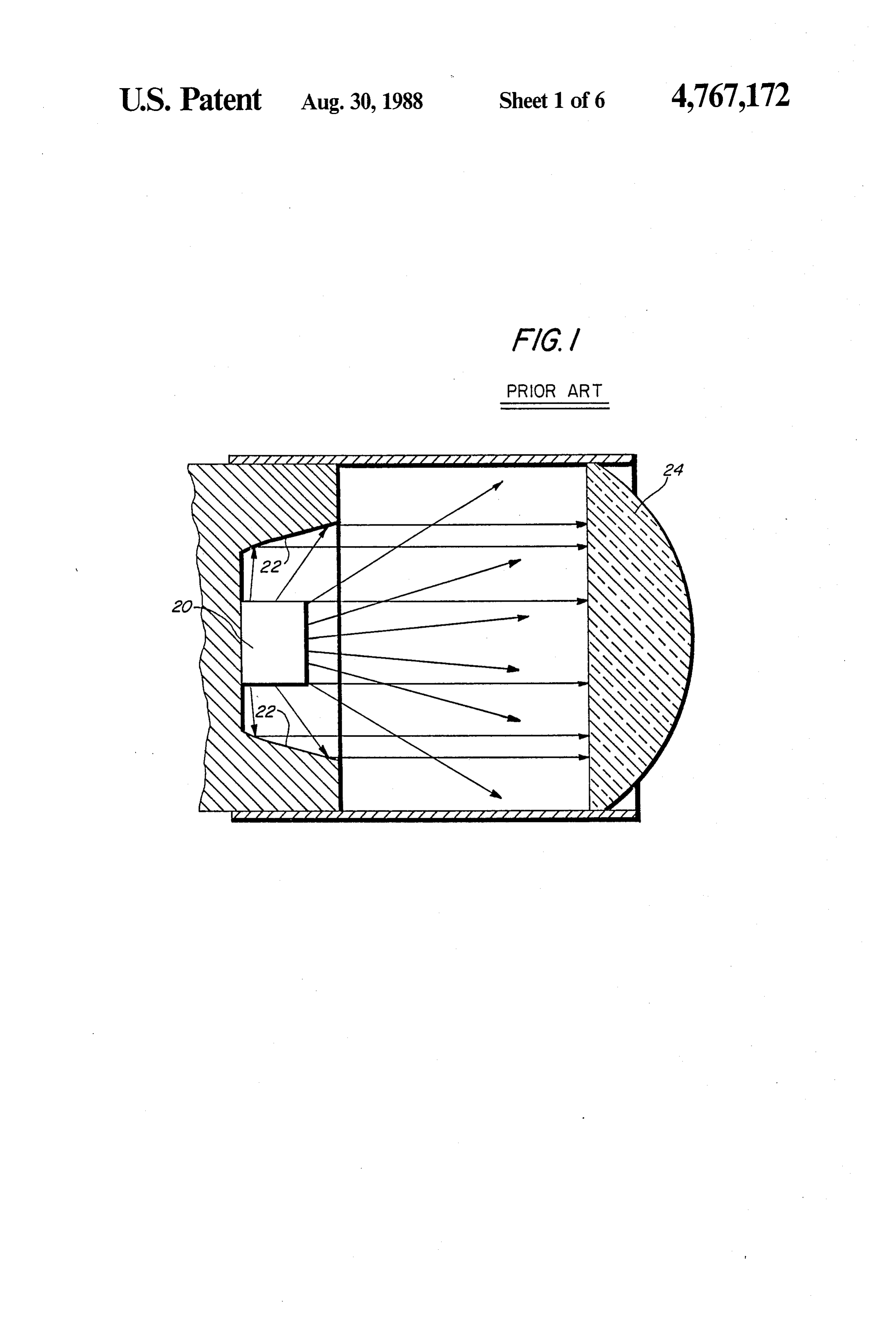
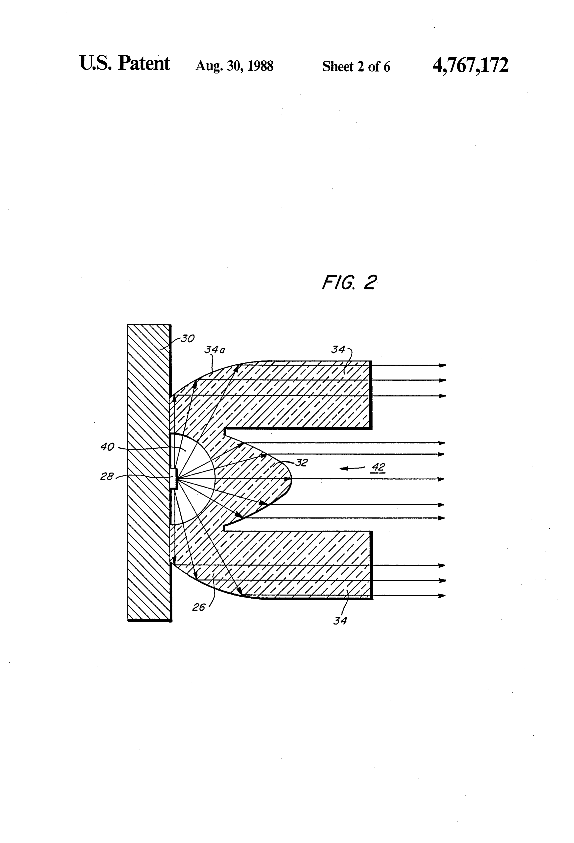
ductor. Generally, since LEDs produce a relatively 50 FIG. 1 is a typical prior art configuration of the small quantity of light as compared to other types of means to capture the light rays emitting from an LED; lamps, LEDs have generally been used with optical FIG. 2 is a profile of a light collector in accordance wave guides to transmit a sufficient amount of light to with the present invention.
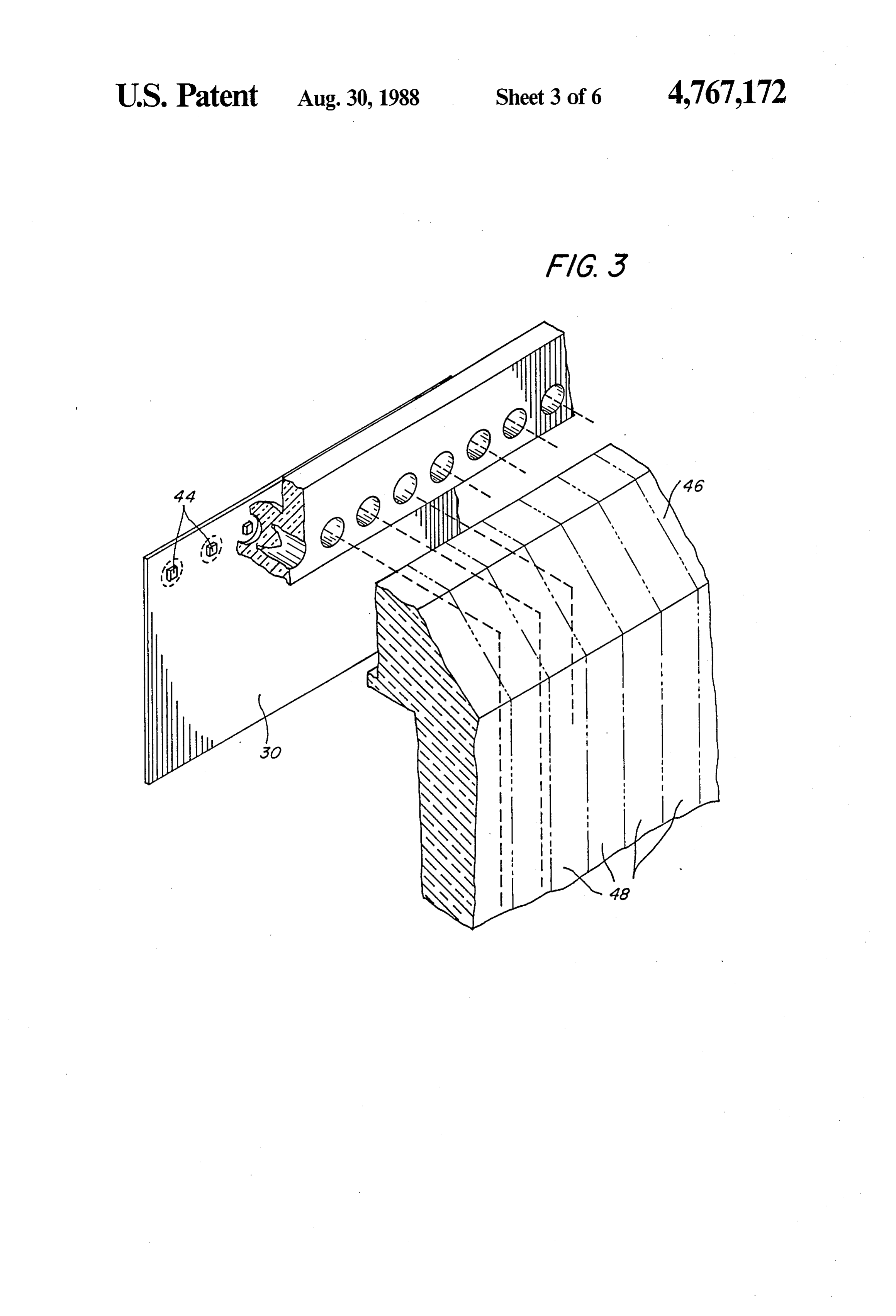
the photoconductor. It is taught in U.S. Pat. No. FIG. 3 is an isometric drawing illustrating the LED 4,255,042 to provide a light channel having one end 55 array and segmented light pipes;
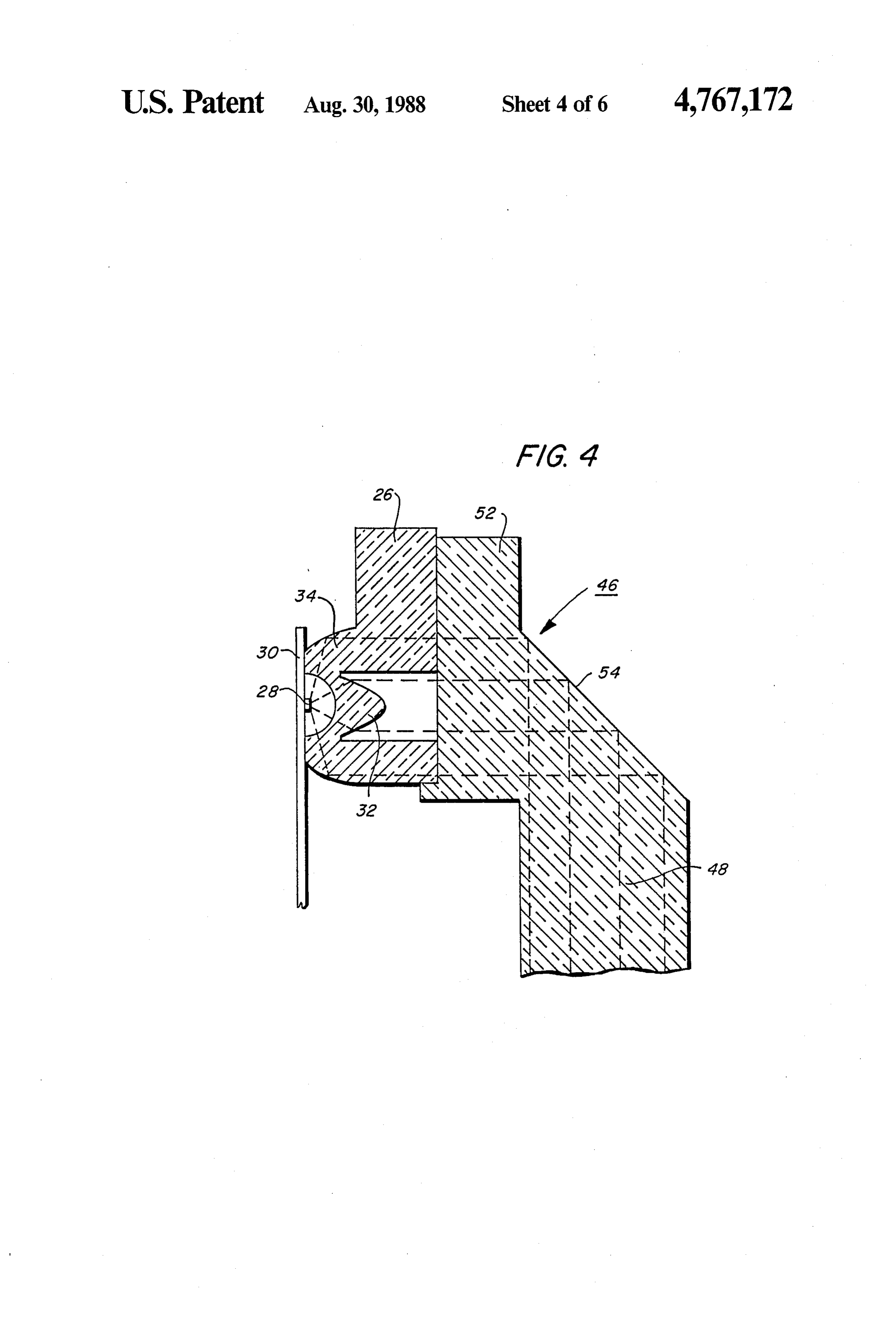
next to an array of discrete light emitting diodes for FIG. 4 is a sectional view of the relationship of an channeling the light to a photoconductive surface lo LED, the light collector, and the light pipe in accor cated at the opposite end of the channel. Light is emit dance with the present invention;
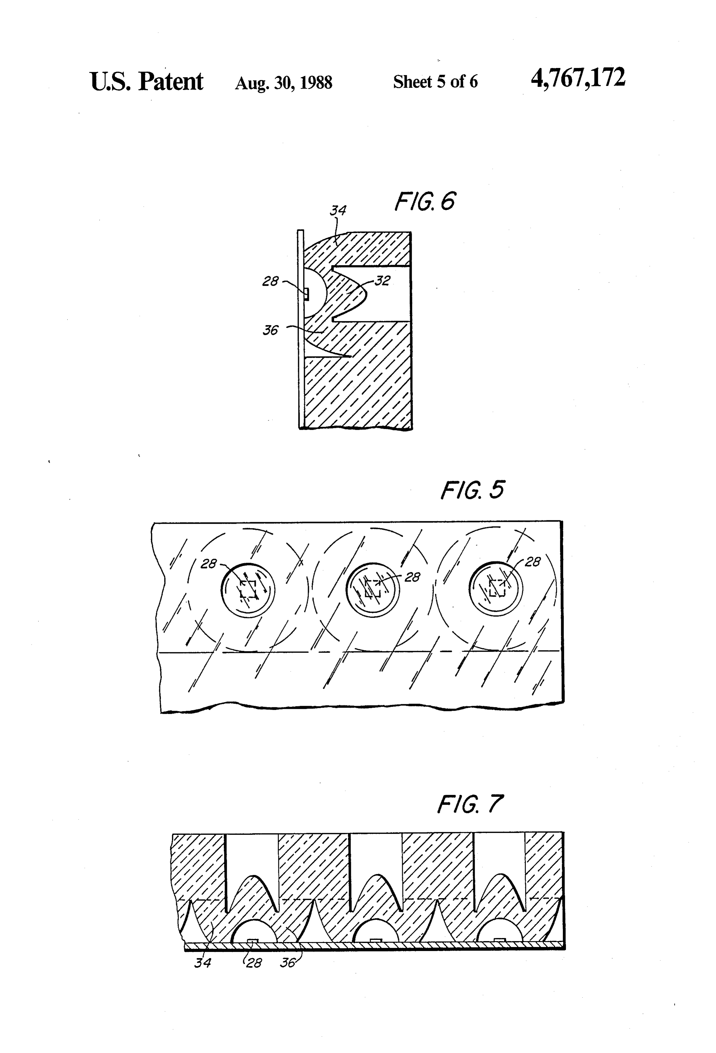
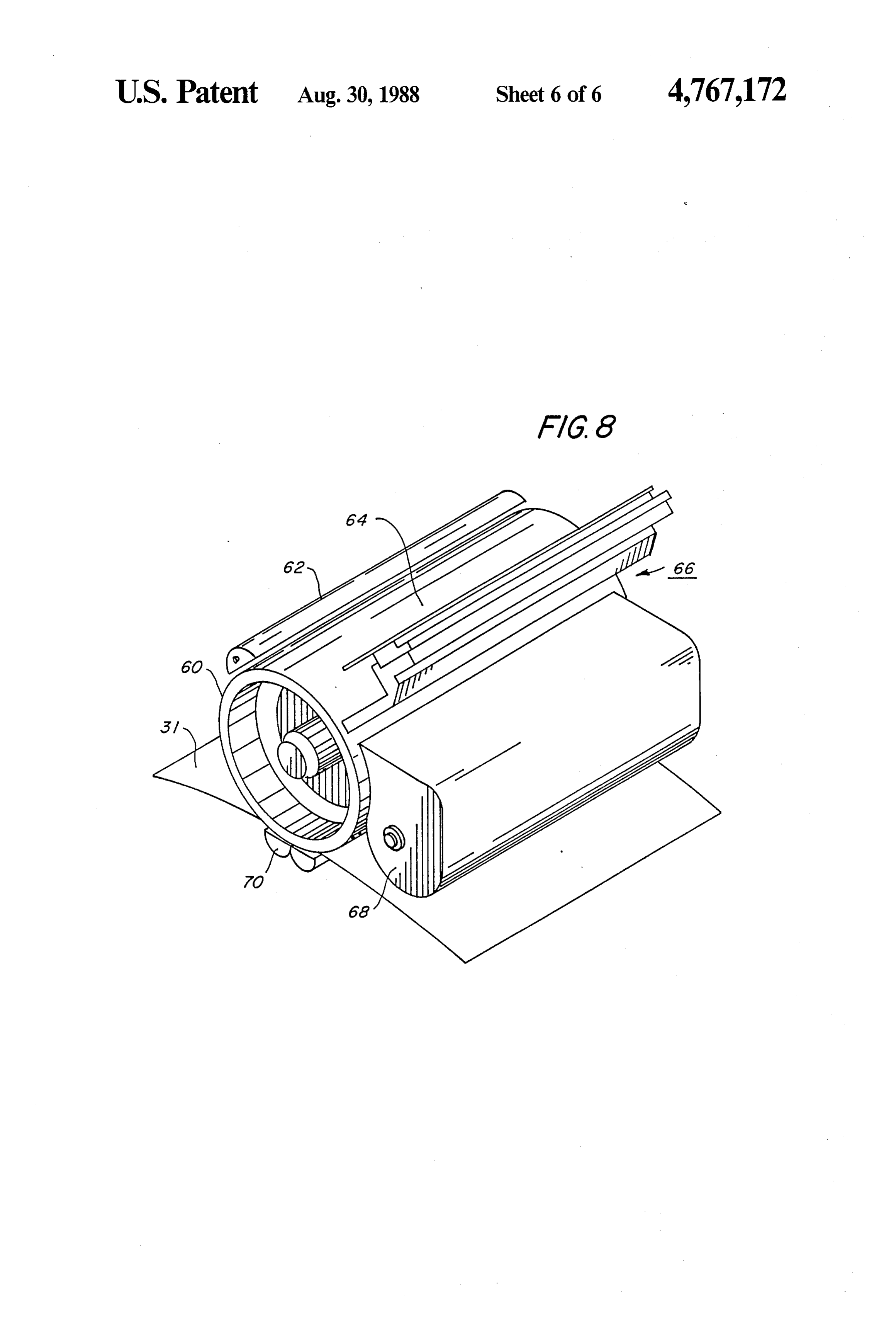
ted from the LEDs into the light pipes and internally FIGS. 5, 6 and 7 are a top view, end view cross sec reflected and propagated down the light pipes to the tion and side view cross section of the LED array and photoconductor. light collector in accordance with the present inven A difficulty with prior art systems using LED arrays tion; and is that there is generally a loss of edge light that is not FIG. 8 is an illustration of the LED array and light captured by the light pipes with the resultant inefficient collector in relation to a photoreceptor surface. light transmission. Another difficulty arises from imper 65 With reference to FIG. 1, there is shown a typical fect or uncollimated light entering the wave guide re prior art device for increasing the light output effi sulting in light exiting the wave guide in an uncon ciency of a light emitting diode (LED). A light emitting trolled fashion and discharging portions of the image. In diode 20 is positioned at the focal point of a suitably
Page 9
coated reflector 22. The light rays emitted from the light rays projecting from the LED 28 are reflected sides of the LED are relected from the reflector 22 into through the leg portion 34 or refracted through the lens a generally collimated light beam. However, the light surface 32 into well collimated, concentric beams of rays emitted from the front of the LED, as illustrated by light that are reflected from the surface 54 into the light the arrows, do not strike the reflector and are therefore pipe 48. It should be noted that the light rays projected scattered and lost. To compensate for those light rays from the LED either from the side or from the top of that are not reflected, it is known to place a suitable lens the LED are reflected by either the legs or refracted by 24 in front of the LED to collect the unreflected rays the lens 32 into two collimated beams. Since the two and produce a collimated beam. Unfortunately, while beams are well collimated, reflection from surface 54 the lens 24 may collimate the scattered light rays, it 10 can be by total internal reflection, thus avoiding the tends to disperse those light rays already collimated by need to coat surface 54 with a reflective material. FIGS. the reflector 22. 5, 6 and 7 show in more detail a top view, an end view In accordance with the present invention, there is cross section and a side view cross section of an LED provided an integrally molded light collector, generally collector array.
shown as 26, for collecting and collimating the light 15 In operation, there is shown in FIG. 8 a photocon rays projected from an LED as shown in FIG. 2. In ductor 60 in an electrophotographic process. The pho particular, an LED28 is suitably mounted on a substrate toconductor 60 is illustrated as rotating in a clockwise 30. The integral collector 26 is preferably any appropri direction to receive first a uniform charge under a ate transparent plastic material such as styrene, acrylic charging device 62. Upon receiving an image at station or polycarbonate. The collector is comprised of a con 64, the photoreceptor continues to rotate to the LED vex center lens portion 32 with a concentric surround array and segmented light pipes illustrated at 66. By ing leg portion 34 appending therefrom. An edge por selective activation of LEDs, the light pipes can be used tion of the leg 34 is rigidly secured to the substrate 30 to discharge edge portions or pitch portions on the concentric with the LED 28. Preferably, substrate 30 is photoreceptor surface or to provide a test patch for a porcelain coated metal or ceramic material. A semicir system correction. Next, the photoreceptor advances to cular air pocket 40 separates the LED 28 from the col 25 the development station illustrated at 68 at which toner lector 26. The cavity around the LED provides me is placed on the image and on the test patch if present, chanical protection and insulation from dirt and other and then to the transfer station 70 at which the image is foreign particles that might diminish light output. It transferred to a copy sheet. Not shown are the usual should be noted the cavity or air pocket 40 could be steps of fusing of the image to the copy sheet and the filled with any suitable optical transparent filler in order 30 placement of the copy sheet in an output tray. to increase the output of the LED through index of While there has been illustrated and described what is refraction matching. Another air pocket 42 is formed at present considered to be a preferred embodiment of between the leg 34 and the lens 32.
In operation, light rays projected from the sides of the present invention, it will be appreciated that numer the LED 28 traverse the air pocket 40, enter the end 35 thosechanges ous and modifications are likely to occur to portion of the leg 34 and are reflected from the para pended claimsintothe skilled cover art, and it is intended in the ap all those changes and modifica bolic outside surface 34a of the leg 34 and form gener tions which fall within the true spirit and scope of the ally parallel light paths or collimated beans of light present invention.
through the leg 34. Light rays projected from the top of the LED 28 traverse the air pocket 40 and enter portion 40 What 1. A is claimed is:
molded light collector for collimating the light 32. The convex surface lens 32, as illustrated, refracts the light beams into a collimated beam into and through source for coupling toa anrelatively rays emitting from optical wide emission light wave guide, the light the air pocket 42.
In a preferred embodiment, an array of LEDs is used source being an LED mounted on a substrate, the light in a strip to selectively dissipate the charge on a photo 45 collector enclosing the LED and forming a hemispheri receptor. With reference to Figure 3, there is shown a cal cavity around the LED, a portion of the light collec substrate 30 supporting a plurality of LEDs 44 aligned tor being integrally secured to the substrate, the light with an optical wave guide 46 comprising a plurality of collector comprising light pipes 48. The optical wave guide 46 is rigidly an optical wave guide, secured to the substrate 30, in order that one end of each a lens portion for collimating the light exiting from of the segmented light pipes 48 is securely fastened in 50 the light source substantially perpendicular to the alignment with one or more of the LEDs 44. Light substrate, and pipes of various widths could be provided in alignment a reflecting portion attached to the substrate for colli with one or more LEDs to perform designated func nating the light exiting from the light source sub tions. For example, light pipes could be used for edge 55 stantially parallel to the substrate, the hemispheri fadeout, pitch erase, and patch generators in an electro cal cavity forming an air pocket between the LED photographic machine. and the light collector wherein the collimated light With reference to FIG. 4, there is shown in more beans are combined and applied to the optical detail the alignment of the optical wave guide with the wave guide.
substrate supporting the LEDs. In particular, an LED 2. The light collector of claim 1 in which the lens 28 is shown mounted on substrate 30. Also secured to 60 portion is a convex lens collimating the light exiting the substrate 30 is the collector 26 connected to the from the light source within an approximately 40 cone optical wave guide 46. It should be understood that the relative to a perpendicular to the substrate. collector 26 is an integral unit comprised of several 3. The light collector of claim 1 wherein the reflect subassemblies having a lens portion 32 and a leg portion ing portion is a parabolic reflector for collimating the 34, although only one assembly is illustrated in FIG. 4. 65 light rays emanating from the light source at an angle The optical wave guide 46 includes a connector por from 45 to 90 relative to a perpendicular to the sub tion 52, a reflector surface 54 and a light pipe portion 48 Strate.
terminating adjacent to a photoreceptor surface. The st is
Provenance
- Collection
- Cited prior art
- Original PDF
- patentimages.storage.googleapis.com →
- Filed
- 1985-03-11
- Pages
- 9
- Method
- pdftotext (the PDF's own text layer) + pdftoppm 300dpi page scans
- Source
- Google Patents bibliographic record
- Granted
- 1988-08-30
- Inventors
- Virginia R. Nichols; Fred F. Hubble, III; James P. Martin; Xerox Corp
- Transcribed from
- patentimages.storage.googleapis.com →