patent · US4289797
Method of depositing uniform films of Six Ny or Six Oy in a plasma reactor
15 September 1981
Page 1 — bibliographic record
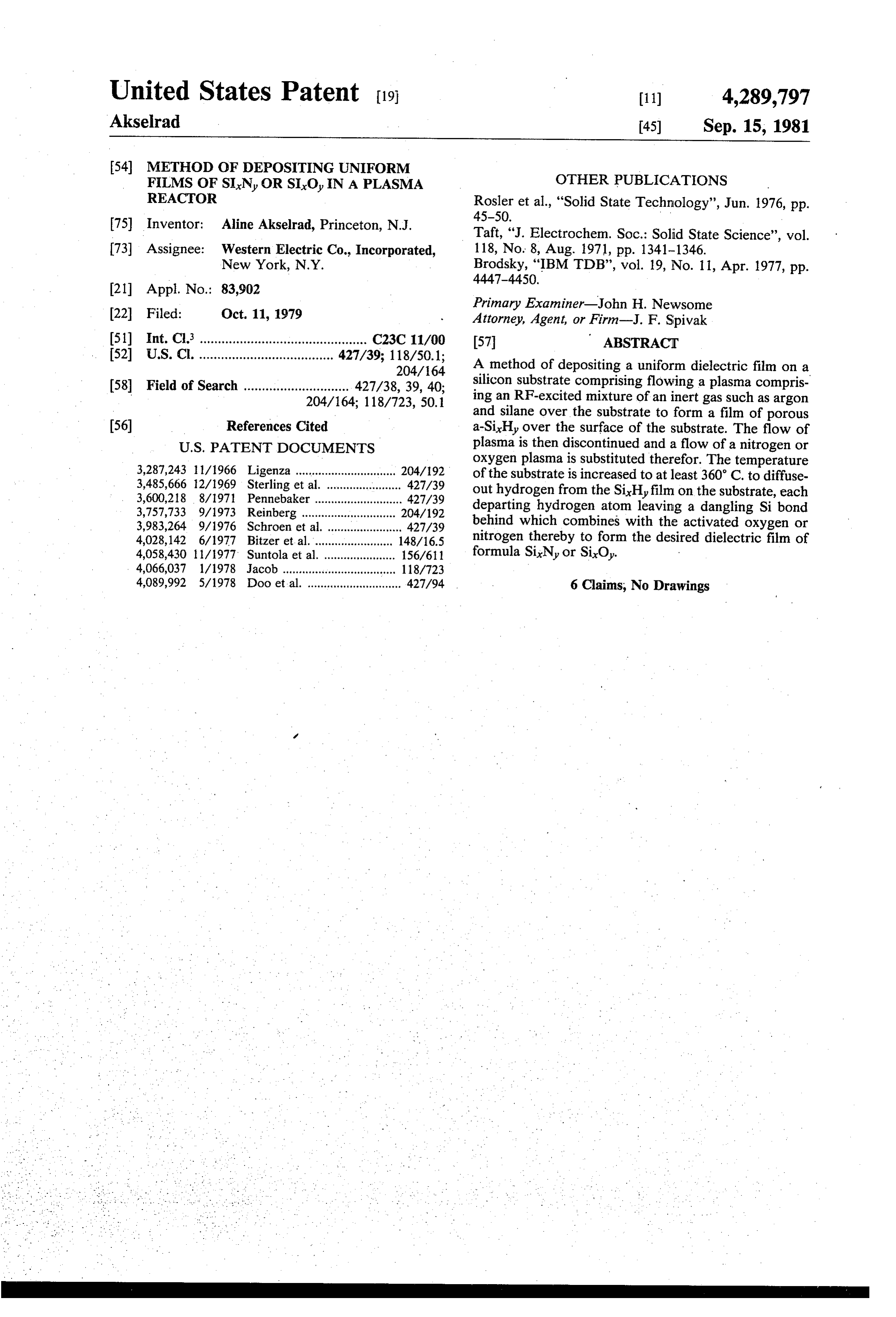
United States Patent (19) 11) 4,289,797 Akselrad 45) Sep. 15, 1981
54 METHOD OF DEPOSITING UNIFORM
FILMS OF SIN, OR SIO, IN A PLASMA OTHER PUBLICATIONS REACTOR Rosler et al., "Solid State Technology", Jun. 1976, pp. o 45-50.
75) Inventor: Aline Akselrad, Princeton, N.J. Taft, "J. Electrochem. Soc.: Solid State Science', vol. 73 Assignee: Western Electric Co., Incorporated, 118, No. 8, Aug. 1971, pp. 1341-1346. New York, N.Y. EBM TDB", vol. 19, No. 11, Apr. 1977, pp. 21 Appl. No.: 83,902 --JV.
21 App Primary Examiner-John H. Newsome 22 Filed: Oct. 11, 1979 Attorney, Agent, or Firm-J. F. Spivak 51) Int. Cl. .............................................. C23C 11/00 57 ABSTRACT 52 U.S.C. ..................................... 427/39; "E: A method of depositing a uniform dielectric film on a silicon substrate comprising flowing a plasma compris (58) Field of Search ................. 204/163. ing an RF-excited mixture of an inert gas such as argon s ww and silane over the substrate to form a film of porous 56) References Cited a-Si-Hy over the surface of the substrate. The flow of
w oxygen plasma is substituted therefor. The temperature 3,287,243 ll/1966 Ligenza ............................... 204/192 of the substrate is increased to at least 360° C. to diffuse
elileOakc. . . . . . . . . . . . . . . . . . . . . . . . . . . .
out hydrogen from the Six Hy film on the substrate, each
3,983,264 9/1976 Schroen et al. ....................... 427/39
it thereby to form the desired dielectri YE f 4,028,142 6/1977 Bitzer et al...... 148/16.5 nitrogen thereby to form the desired dielectric film o 4,058,430 1 1/1977 Suntola et al. ... 156/6 formula Six Nyor SiOy.
4,066,037 1/1978 Jacob ........... ... 118/723 4,089,992 5/1978 Doo et al. ............................. 427/94 6 Claims, No Drawings
Page 2
METHOD OF DEPOSTING UNIFORM FILMS OF DETALED DESCRIPTION SIN, OR SIO, IN A PLASMA REACTOR The instant invention provides for the plasma deposi tion of denser, and more uniform films of Six Ny, Six
TECHNICAL FIELD NO, or SiOyin a two-step process utilizing successive Broadly speaking, this invention relates to plasma one-component plasmas.
deposition. More particularly, in a preferred embodi As an example, consider the deposition of SiNy. First, using an entirely ment, this invention relates to a method of depositing a plasma reaction chamber, or conventional Reinberg-type two-component film of material from successive, one 10 equivalent, a thin, uniform component gas plasmas. film of Si-Hy is deposited on a silicon substrate using an RF-excited SiHy--Argas plasma. The Reinberg reac
BACKGROUND OF THE INVENTION tion chamber is described in U.S. Pat. No. 3,757,733 Plasma deposition is a technique that is widely used in which issued on Sept. 11, 1973 to A. R. Reinberg, which patent is hereby incorporated by reference as if more industry to deposit thin films of material on a variety of 15 fully set forth herein. The ratio of y/x in the deposited workpieces. For example, in the manufacture of inte Six Hy film is adjusted by controlling the temperature of grated circuits, an RF-excited plasma comprising an the inert gas, such as argon, and the reactive species silane, and substrate,
which will typically fall between 50 C.
(SiH4) and ammonia, (NH3) is used to deposit a thin The Si-Hy film that is deposited is actually a porous, film of SiN, the designation given to compositions ap 20 amorphousa-Si-H film with its porosity and total hy proaching Si3N4 but not necessarily identical with drogen content being primarily determined by deposi Si3N4, on a silicon wafer approximately 3 inches in tion temperature, deposition rate and the RF power diameter. The SiN film can then be used as mechanical which is applied to the reaction chamber. The proper protection during subsequent processing of the wafer, ties of thin films of a Si-H are described in "Infrared as a dielectric insulating layer between 2 layers of metal 25 and Raman Spectra of the Silicon-Hydrogen Bonds in lization, or (if improved) as a hermetic seal. Amorphous Silicon Prepared by Glow Discharge and It will be appreciated that among the desirable prop Sputtering' by M. H. Brodsky, M. Cardona and J. J. erties that must be possessed by such a silicon nitride Cuomo, Phy, Rey, B., Vol. 16, No. 8, 15 October 1977 at film are uniformity of thickness, uniformity of composi Pg. 3556; “Properties of Amorphous Silicon and a-Si tion and freedom from defects such as impurities and 30 Solar Cells' by D. E. Carlson, C. R. Wronski, J. I. pin-holes. Unfortunately, the prior art plasma deposi Pankove, P. J. Zanzucchi and D. L. Staebler, RCA tion processes are unpredictable and such undesirable REview, Vol. 38, June 1977, pp. 211-225 (Table I at Pg. defects are quite common, occurring randomly, for no 217 in particular); and "Controlling the Type of Bonded apparent reason. - Hydrogen Sites in Glow-Discharge Amorphous Silicon One mechanism that has been proposed to explain at 35 Films' by M. H. Brodsky, IBM Technical Disclosure least some of the observed defects is a reaction of the Bulletin, Vol. 19, No. 11, April 1977, pp. 4447–4450, all form: of which references are hereby incorporated by refer ence as if more fully set forth herein.
(SiH)4+(NHm")B-(Si-NH2)C+other fragments After an appropriate time interval, the flow of SiH . 40 4+Ar is replaced by a flow of N2, or other suitable where nitrogen-containing mixture.
ns 4 and ms3, Because the flow of SiH4 has been terminated, its where * indicates some metastable excited configura premature decomposition is no longer a problem; thus, tion and where the component SiN.H., can be in an the pressure, the frequency of the RF-excitation and/or excited state or in a ground state, the said reaction 45 the input power to the reaction chamber may be in taking place in the plasma rather than on the sur creased to a point where activated nitrogen is produced face of the substrate. in the chamber. Next, the temperature of the substrate is As might be expected, such a reaction would produce raised to more than 360° C. so that hydrogen starts to particulate matter that would deposit onto the surface diffuse out of the Si-H.
of the substrate. One reason that has been suggested for 50 the departing hydrogenSince a-Si is porous, and since leaves behind dangling Si the occurrence of this reaction is that, once a molecule bonds, the diffusion of activated N. into Si and the for of Six-NH2 has formed in the plama, it provides all of mation of Si-N bonds is accelerated, thus forming a the incentives for plasma deposition that the substrate uniform, impurity-free, dielectric film of SiN. itself provides. If extremely uniform layers of SixNy are required, the SUMMARY OF THE INVENTION 55 process may be modified by laying down a very thin layer of a-Si-H and repeating the procedure several
As a solution to this problem, I propose a method times until the desired overall thickness is obtained. As wherein a thin, uniform film of porous a-Si-Hy is depos an alternative, one could start the process by depositing ited on a silicon substrate by means of a one-component plasma comprising a silicon-containing active radical, 60 aand thin layer of SiN.H., which is porous and N-deficient complete the nitridation in a N* rich plasma by such as silane or silicon tetrachloride. After the porous adding some nitrogen-containing compound to the ini film has been deposited, this one-component plasma is tial gas plasma. However, the possibility of non withdrawn and the film oxidized or nitrided in situ by flowing activated oxygen or nitrogen over the sub uniformity The remains with this alternate embodiment.
above-described process has the following ad strate. 65 vantages: - -
The invention and its mode of operation will be more 1. In a simple plasma reactor, the uniformity of a fully understood from the following detailed descrip one-component film, such as Si, is more easy to obtain
than the uniformity of a film which is deposited from a
Page 3
mixture of two gases which differ in activation energy, SixHy film, each departing hydrogen atom leaving for example, SiH4 and N2 or SiH4 and NH3; behind a dangling Sibond which combines with an 2. More complex compositions and layer structures excited radical of the activated gas in said second can be attempted sequentially; plasma thereby to form said dielectric film of for 3. If the diffusion of the active radical (N*) into Si mula SiM, where M represents either oxygen or layer dominates, the film will be denser than ordinary nitrogen, depending on the identity of said acti SiN and it is possible that the tensile stress will decrease; Vated gas.
and 4. Homogenous nucleation of Si-NH2 and the result substrate 2. The method according to claim 1, wherein said ing particle contamination are eliminated. 10 is physically located within an RF-excited, One skilled in the art will appreciate that, by substi plasma reaction chamber and the gas which comprises tuting a flow of activated oxygen for the flow of acti said second excited plasma is activated by increasing the vated nitrogen in the above-described process, the film level of the RF power supplied to the reaction chamber that would ultimately form on the substrate would be over that which was supplied to excite the mixture of SiOy rather than SiN. Similiarly, by flowing simulta 15 the inert gas and the volatile Si compound. neously both nitrogen and oxygen, the film would com 3. The method according to claim 1, wherein said prise SiNOz. It will also be appreciated that while substrate is physically positioned within an RF-excited, RF-excitation of the plasma is the preferred embodi plasma reaction chamber and the gas which comprises ment, other forms of excitation are possible. Likewise, the second excited plasma is activated by changing the while silane is the preferred embodiment for the first 20 frequency of the RF-excitation to a frequency which is plasma, other volatile Si compounds can be used. above that used to excite the mixture of the inert gas and One skilled in the art may make various changes to the volatile Si compound.
the above-described processes without departing from 4. The method according to claim 1, wherein said the spirit and scope of the invention. substrate is physically positioned within a plasma reac What is claimed is: 25 tion chamber and the gas which comprises the second 1. A method of depositing a uniform dielectric film on excited plasma is activated by adjusting the pressure of a silicon substrate, comprising the steps of: the gas which comprises the second excited plasma to a flowing a first plasma comprising an excited mixture value to permit activation.
of inert gas and a volatile Si compound over said 5. The method according to claim 1, wherein said substrate thereby to form a film having porous 30 substituting step comprises:
a-Si-H over the surface of said substrate; substituting the flow of a second excited plasma com discontinuing the flow of said first plasma and substi prising a mixture of activated oxygen and nitrogen, tuting therefor a flow of a second excited plasma whereby the dielectric film formed on said sub comprising an activated gas selected from the strate comprises Six-NOz.
group consisting of oxygen and nitrogen over said 35 6. The method according to claim 1, wherein said substrate; and then temperature-elevating step comprises raising the tem elevating the temperature of said substrate to cause perature of said substrate in excess of 360° C. the hydrogen to diffuse-out from said porous a ak k k se sk
Provenance
- Collection
- Cited prior art
- Original PDF
- patentimages.storage.googleapis.com →
- Filed
- 1979-10-11
- Pages
- 3
- Method
- pdftotext (the PDF's own text layer) + pdftoppm 300dpi page scans
- Source
- Google Patents bibliographic record
- Granted
- 1981-09-15
- Inventors
- Aline Akselrad; Western Electric Co Inc
- Transcribed from
- patentimages.storage.googleapis.com →