patent · US4226897
Method of forming semiconducting materials and barriers
7 October 1980
Page 1 — bibliographic record
United States Patent (19) 11 4,226,897 Coleman 45) Oct. 7, 1980 54 METHOD OF FORMING 933549 8/1963 United Kingdom ...................... 427/41
SEMCONDUCTING MATER ALS AND
BARRERS OTHER PUBLICATIONS 75) Inventor: John H. Coleman, Locust Valley, Chittick, "Journ. of Non-Crystalline Solids', 3 (1970),
73 Assignee: Plasma Physics Corporation, Locust Primary Examiner-John H. Newsome Valley, N.Y. 57 ABSTRACT 21 Appl. No.: 857,690 In a gaseous glow-discharge process for coating a sub 22 Filed: Dec. 5, 1977 strate with semiconductor material, a variable electric field in the region of the substrate and the pressure of 51) Int. C.’............................................... B05D3/06 the gaseous material are controlled to produce a uni 52 U.S. Cl. ...................................... 427/39; 204/164; form coating having useful semiconducting properties. 427/84; 427/85; 427/86; 427/164 Electrodes having concave and cylindrical configura 58) Field of Search ....................... 427/38, 39, 40, 41, tions are used to produce a spacially varying electric 427/164, 165, 166, 167; 204/164, 165, 168; field. Twin electrodes are used to enable the use of an 357/2, 15 AC power supply and collect a substantial part of the (56) References Cited coating on the substrate. Solid semiconductor material
3,437,511 4/1969 Hough ................................... 427/39 control the discharge and improve the coating.
3,655,438 4/1972 Sterling et al ... 427/39 Schottky barrier and solar cell structures are fabricated 4,059,461 11/1977 Fan et al..... ... 427/86 from the semiconductor coating. Activated nitrogen 4,064,521 12/1977 Carlson .................................... 357/2 species is used to increase the barrier height of Schottky barriers.
FOREIGN PATENT DOCUMENTS
48-2831 1/1973 Japan ......................................... 427/86 38 Claims, 12 Drawing Figures
Page 2
Drawing sheet — no readable text.
Page 3
Drawing sheet — no readable text.
Page 4
Drawing sheet — no readable text.
Page 5
conducting coating over a large area by means of a
METHOD OF FORMING SEMICONDUCTING glow-discharge in which pressure and electric field are MATERIALS AND BARRIERS controlled. Also, the present process relates to the treat ment of a semiconductor surface to increase the
BACKGROUND OF THE INVENTION Schottky barrier voltage when an active conducting
Hydrogenated amorphous silicon films, hereinafter coating is applied. Such treatment may be used on any called a-Si, which are suitable for semiconductor appli semiconductor material, including crystal semiconduc cations have been prepared by a variety of techniques. tors which have conductivities of 100 and 0.01 ohm cm. Chittick, Alexander, and Sterling reported in the Jour O and higher. My coating process and barrier treatment is nal of the Electrochemical Society, Vol. 116, No. 1 (Janu particularly useful for producing a Schottky barrier ary 1969) pages 77-81, in an article entitled "The Prepa solar cell.
ration and Properties of Amorphous Silicon', that an The principle object of the process is to produce a inductively coupled, RF glow-discharge in silane semiconductor and barrier for use in a solar cell. An (SiH4) gas produced low-conductivity a-Si films that other object of the invention is to coat a large-area could be doped with both donor and acceptor impuri 15 substrate with amorphous semiconducting material. Yet ties, thereby changing the a-Siconductivity over a wide another object is to form a Schottky barrier between a range of values. More recently, a-Si films were pro semiconducting material and an active electrode. An duced by evaporating silicon in an atmosphere of hy other object is to dope large area amorphous semicon drogen (H2) and by sputtering silicon in an atmosphere ductor materials to form an ohmic contact with a con of H2--Ar which exhibited similar semiconductor char 20 ducting substrate. Another object is to introduce semi acteristics to those films made from silane in a glow-dis conductor material from a solid-source into a coating charge. being formed by glow-discharge deposition from the Presently, several commercial projects related to the gas-phase.
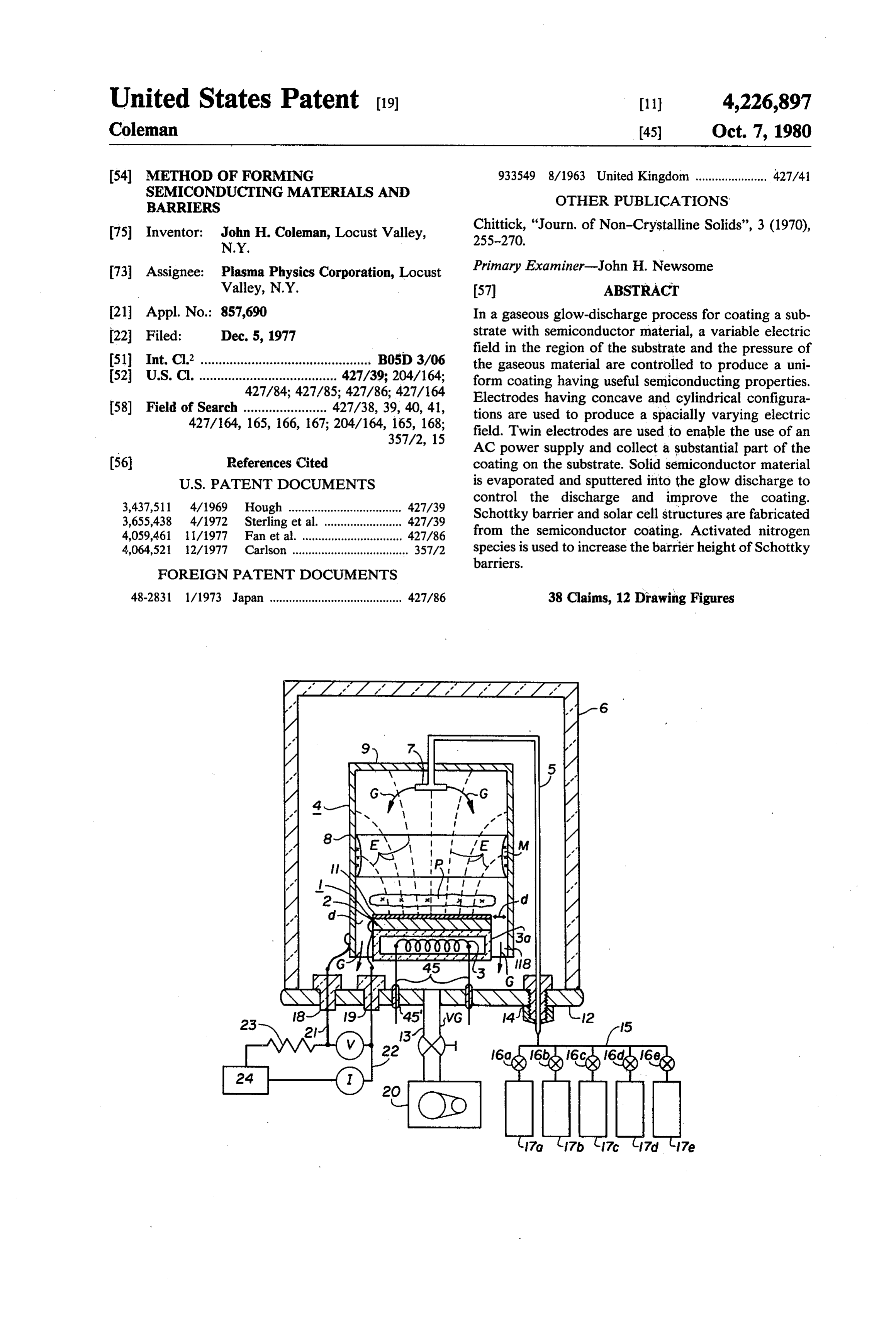
development of Schottky barrier solar cells using crys tal, polycrystal, and amorphous semiconductor materi 25 BRIEF DESCRIPTION OF THE DRAWING als were described in a recent book entitled Twelfth
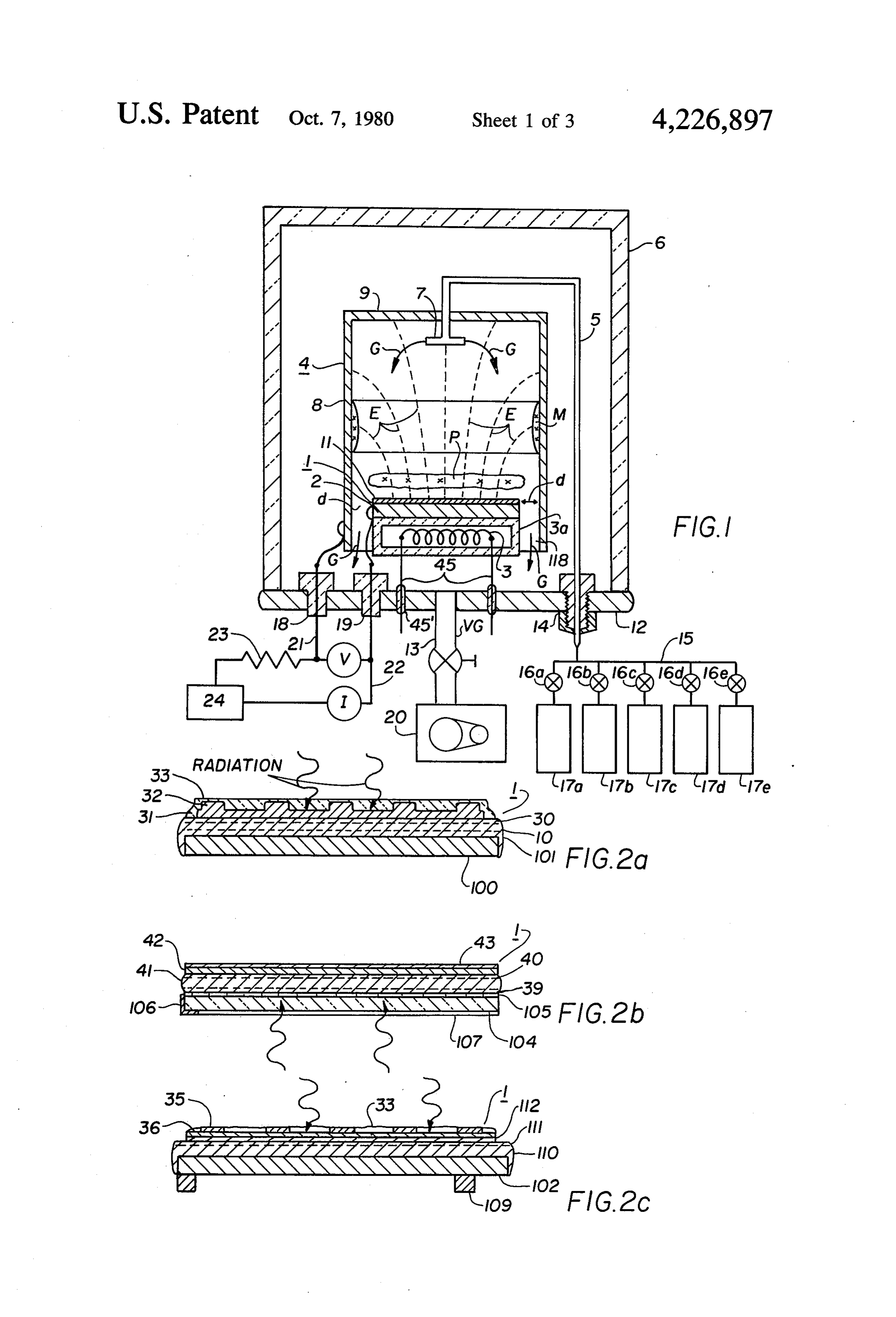
IEEE Photovoltaic Specialists Conference-1976, pub ingFIG. 1 is a cross-sectional view of apparatus illustrat glow-discharge in the weak electric field.
lished by the Institute of Electronic and Electrical En gineers Inc., New York, N.Y., 10017. On pages 893-895 conductor material producedview
FIG. 2 is a cross-sectional of devices using semi of this book, Carlson et al reported in an article entitled treated with activated nitrogen. glow-discharge and
"Solar Cells Using Schottky Barriers on Amorphous
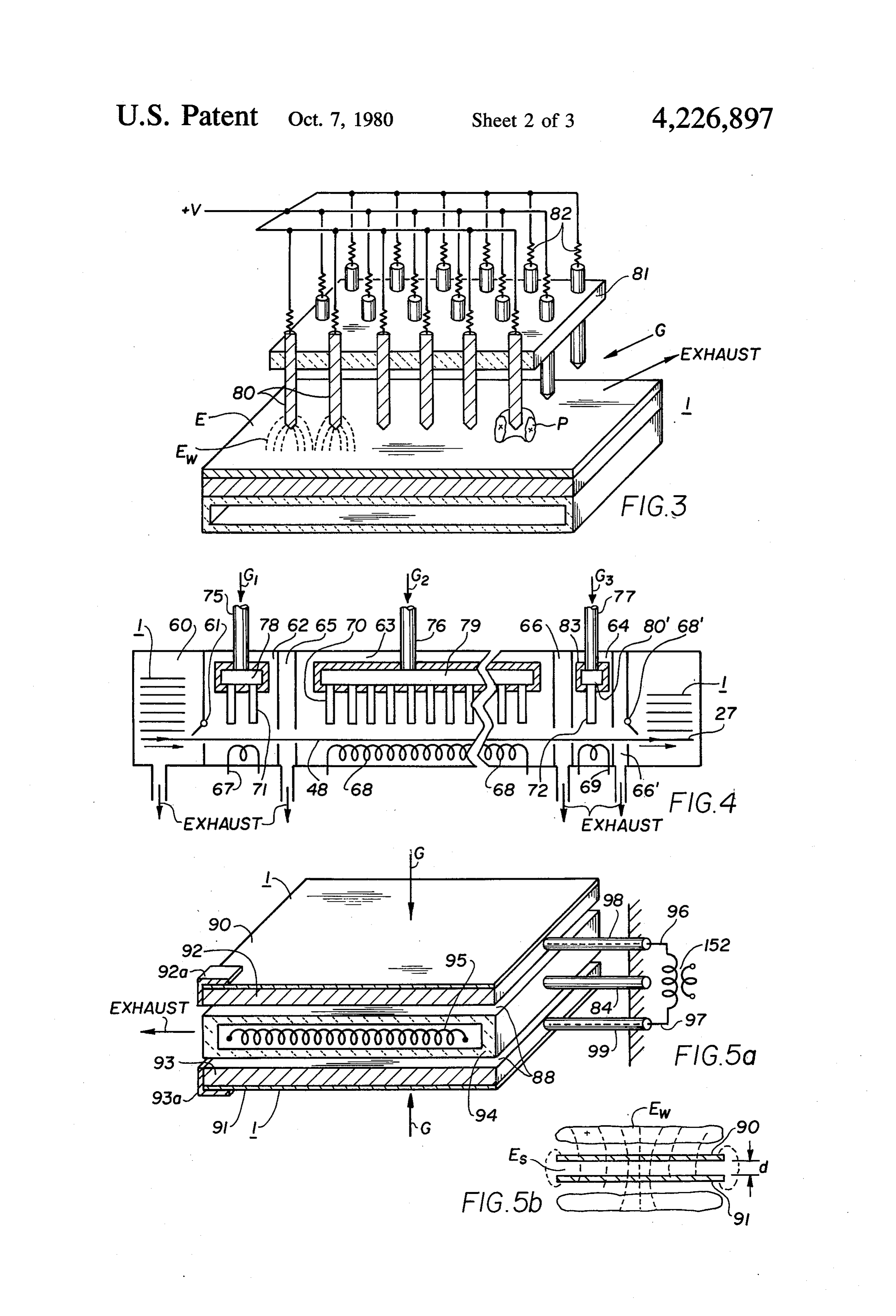
Silicon' that he formed a solar cell by applying a trans tionFIG. in 3 illustrates another embodiment of the inven which multiple electrodes are employed to main parent electrode with appropriate work-function to one tain a glow-discharge.
side of an a-Si film and an ohmic contact to the other.
FIG. 4 illustrates another embodiment in which the
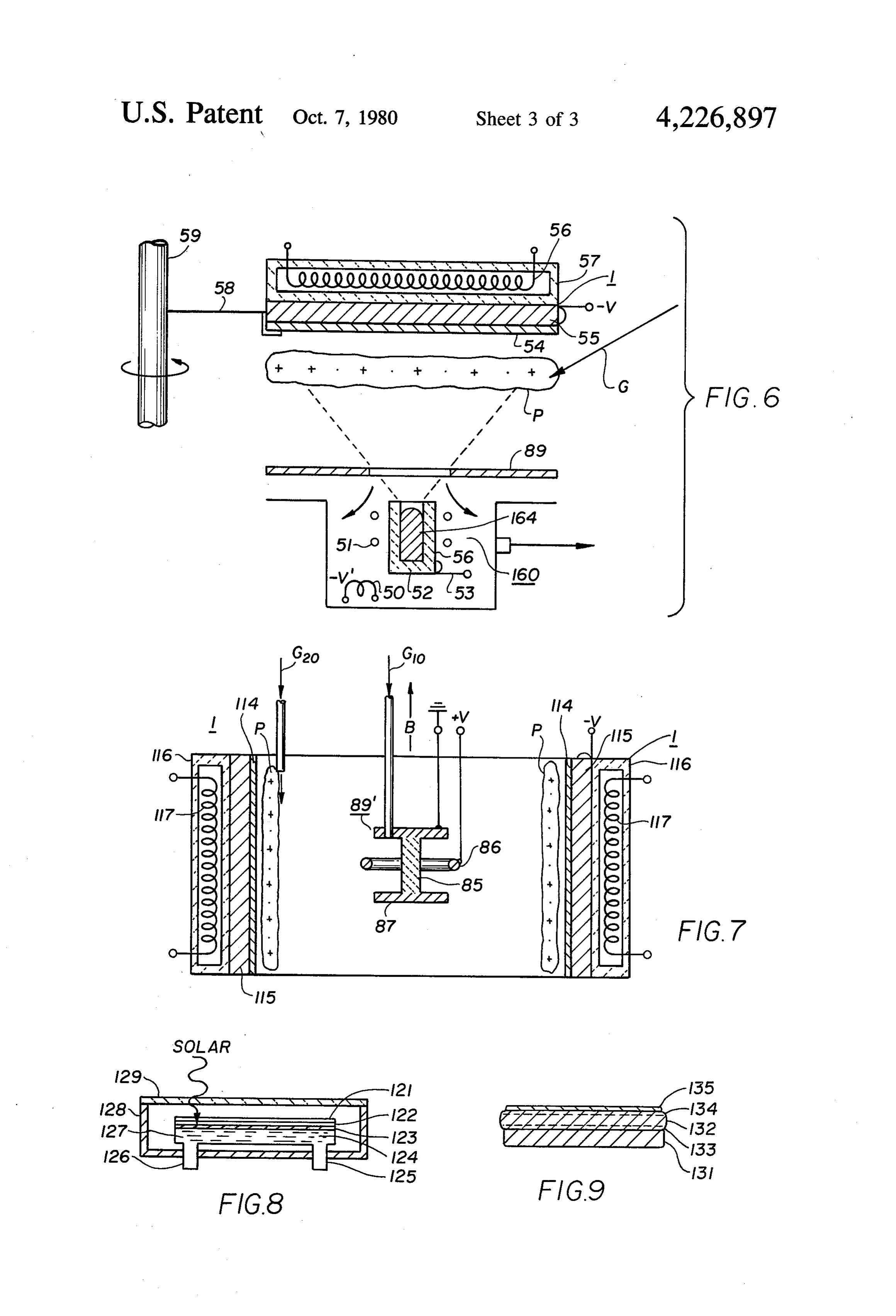
Also, this article stated output voltages increased ini 35 substrate tially by 100 mV when the thin metal electrode was is moved through the glow-discharge. evaporated in residual oxygen background in the vac FIG. 5 illustrates another embodiment in which the uum system, producing a metal-insulator-semiconduc electric field configuration and pressure are adjusted to tor (MIS) structure. More recently, Carlson reported in enable alternating voltages to be applied while collect Vol 77-2 Extended Abstracts, Fall Meeting, Atlanta, 40 ingFIG. a substantial part of the semiconducting material. 6 illustrates another embodiment in which semi
Georgia, Oct. 9-14 1977 of the Electrochemical Society,
Princeton, N.J., 08540, pages 791-792, that these MIS conductor material is evaporated through the glow-dis cells were generally unstable. Furthermore, Carlson charge to stabilize the discharge and attain desired semi reported that his electrodes were less than 0.02 cm2 in conducting properties.
area-a value too small for commercial use. Also, an 45 FIG. 7 illustrates another embodiment in which semi article by Godfrey & Green in Applied Physics Letters conductor material is sputtered through the glow-dis Vol 31, No. 10, (15 Nov. 1977) pages 705-707, indicates charge to stabilize the discharge and attain desired semi that such small areas lead to erroneous data. conductor properties.
My prior glow-discharge coating processes are cov DESCRIPTION OF THE APPARATUS AND ered in U.S. Pat. Nos. 3,068,283, 3,068,510 (Dec. 18, 50 TECHNIQUES
generally related to polymeric coatings which have Referring to FIG. 1 and FIG. 2a, cross-sectional resistivities greater than 1012 ohm-cm High-resistivity views are illustrated of the glow-discharge apparatus coatings act as blocking capacitance in series with the and a typical device made therein. The substrate 1 is a glow-discharge thereby assisting in regulation of coat 55 0.010" thick stainless-steel plate 11 with rectangular ing uniformity. However, neither 60 Hz line transform dimensions of 3"x4" supported by electrode 2. Resis ers nor DC power supplies can be used with my prior tance heater 3 is embedded in ceramic block 3a which processes. The present process, on the other hand, pro supports and heats electrodes 2, 11. Substrate 1 is posi duce semiconducting films which act primarily as resist tioned in the open face of concave counter electrode 4 ances in series with the glow discharge and which re 60 which has a rectangular cross-section of 4'x5' defined quire different process concepts. by side-walls 8 and top 9. Top 9 is positioned at least 4" above the front surface of substrate 11. Electrode as
SUMMARY OF THE INVENTION semblies 1 and 4 are positioned inside an enclosure 6 and The present coating process is related to producing header 12 and are joined by appropriate gasket to form semiconductor films which have electrical resistivities 65 a gastight seal. Vacuum pump 20 is connected through generally less than about 1012 ohm-cm at room-tempera valve and nipple 13 to header 12 to evacuate enclosure ture, and preferably between 1012 and 106 ohm-cm. The 6. Gases G from tanks 17 a-e are conducted through present process is designed to produce uniform semi regulated needle valves 16 a-e, manifold line 15, and
Page 6
connector 14 through header 12 into enclosure 6. Here, potential difference V is applied between electrodes 2, 4 gases G are conducted through dielectric tubing 5 and of about 350 volts and I of 5 mA to 10 mA to produce diffusor 7 inside electrode 4. A gap 118 of say 'be a glow-discharge adjacent coated substrate 1. Valve 16c tween walls 8 and electrode 2 permits egress of gases G is closed, the residual gases in enclosure 6 evacuated by after passing through glow-discharge P. Gauge VG 5 pump 20, and the enclosure 6 is backfilled with nitrogen meters the evacuation of enclosure 6 and pressure of from tank 17d (valve 16d) to purge unreacted silane. gases G. Gauge VG is preferably of the capacitance Valve 13 is closed, jar 6 raised to atmospheric pressure manometer type which is commercially available for and substrate 1 removed.
use with corrosive, condensible gases in the range of Referring to FIG. 2a, the substrate 1 is illustrated 0.001 to 10 Torr. Readings from gauge VG may auto 10 with foil 100 coated with n-doped a-Si layer 101, matically regulate valves 16 through a servo-mech undoped 1-4 um a-Silayer 10 and ammonia-treated anism to maintain a desired pressure. A potential V is layer 30. The substrate 1 is then placed in a conven applied between electrodes 2, 4 from power supply 24 tional vacuum-evaporator and coated with a high work by leads 21, 22 connected through insulated electrical function, semi-transparent metal 31 (such as palladium) bushings 18, 19 sealed in header 22. Protective network 15 to a thickness of about 100 A or less to complete the 23 prevents damaging sparks. Voltage V and current I Schottky barrier. The conducting layer 31 is adjusted to are metered as indicated. Resistance heater 3 enclosed be thick enough to reduce its sheet resistance while not in ceramic 3a is connected through leads 45 and electri absorbing an inordinate amount of incident photons. A cal bushings 45' to an appropriate power source (not grid 32 of thicker metal such as a silvertitanium alloy shown). m (Ag-Ti) is applied to reduce the series resistance of the In operation, the enclosure 6 is evacuated by pump 2 semi-transparent electrode 31. Also, a top antireflection to a pressure below about 0.02 Torr and back-filled with (AR) layer 33 such as Si3N4 with a thickness range of silane (SiH4) from tank 17a by opening valve 16a. Valve about 1000A may be applied to electrode 31 to reduce 16a is adjusted to maintain the desired pressure in enclo reflection loss under photon irradiation. Under test sure 6 which, for example, may be Torr. Next a mix 25 using AM1 illumination and a Tektronics Corp. curve ture of 10% phosphine (PH3) in helium (He) from tank tracer, the short-circuit current Isc was measured to be 17b is admitted into manifold 15 where it mixes with about 2 mA/cm2 and the opencircuit voltage Voc was silane and flows through lines 5, 7 to raise the system about 350 mV, with no AR coating and 50% reflection pressure PG to about 1 Torr. The potential difference V loss. When the NH3- treated layer 30 was added to the between electrodes 2, 4 is adjusted to about 530 volts 30 a-Si and a semi-transparent electrode layer 10 was ap initiating a glow-discharge and the current, I, adjusted plied as described above, the short-circuit current Isc to about 5 mA, to produce a heavily doped in coating remained about 2 mA/cm2 under illumination while the on plate 11 which is schematically illustrated in FIG.2a open-circuit voltage Voc was measured to be greater by coating 101 on plate 100. After maintaining the dis than 600 mV-an increase in excess of 250 mV over that charge for about 1 minute, valve 16b is closed to shut off 35 measured in the preceding test described above with the the flow of PH3 and He leaving silane alone. The unifor undoped surface of the a-Si layer 10 alone, all values mity and impurity level of ohmic-layer 101 is not as being measured without AR coating. Similar increases critical as that of the high-resistivity a-Si layer 10. were found with other substrates as illustrated in the Therefore, ohmic-layer 101 may be deposited by con following drawings.
ventional, doped chemical-vapor-deposition (CVD) or 40 Referring to FIG. 2b, a glass substrate 104 coated other techniques prior to insertion in the apparatus of with a transparent conducting coating 105 of the oxides FIG. 1. of indium (In) and tin (Sn) (commercially available) Next, the pressure PG of silane is adjusted to 0.3 to may be inserted into the apparatus of FIG. 1 on elec 0.4 Torr to position a diffuse discharge P in the region trode 2 with the conducting coating 105 facing the above plate 11 or its equivalent such as illustrated in 45 discharge and conducting tab 106 contacting electrode FIG. 2a by plate 100 and minimize the discharge in the 2. Thereafter, the coating procedure is the same as that region of closest separation d between electrodes 2, 4. described in connection with FIG. 2a, in that ohmic The discharge then occurs in the weaker region of the contact layer 39, a-Si layer 41, NH3-treated barrier electric-field E as will be discussed in more detail in layer 40 are produced sequentially. Also, using an evap connection with FIG. 5b. Deposit M occurs on the 50 orator, a Pd coating 42 is applied to complete the inside wall 8 as shown schematically in FIG. 1 and is Schottky barrier and a thicker metallic layer 43 such as conducting when wall 8 is anodic and unheated as dis Ti-Ag applied to complete the contact. When substrate cussed below in connection with FIG. 3. Of course, on 1 is illuminated (in operation) through the glass sub the alternate polarity cycle of supply 24 when wall 8 is strate 104, electrode 43 may be opaque. An additional cathodic coating M is formed in the weaker compo 55 AR coating 107, such as an oxide of tantalum, may be nents of the electric field as indicated. Coating M has applied to the glass. Although the glass substrate 104 similar properties to those coatings on electrode 11 serves as a useful protective material, the configuration when all process conditions are similar to those de of FIG.2b produces somewhat less output than that of scribed above. i.e. when heated by heaters (not shown) FIG. 2a since the maximum number of charge carriers and when the discharge is restricted in the strong elec are generated at the ohmic surface where the incident tric field across the separation "d'. The discharge is photons impinge first rather than at the barrier where maintained for 20-40 minutes at 5 mA to 10 mA (0.1 to the output potential is developed. 0.2 mA/cm2) with V in the range of 500-1500 depend Referring again to FIG. 2a, b, p-type a-Si may be ing on PG. After desired thickness on substrate 1 is substituted for the n-type a-Si in coatings 10, 41 by attained, valve 16b is closed and the residual gases evac doping with a donor impurity during formation in the uated to background by pump 20. Valve 16c on ammo apparatus in FIG. 1. For example, during formation of nia (NH3) tank 17c is opened to admit NH3 into the the a-Si coating 10, the apparatus of FIG. 1 may be substrate region 1 to a pressure of about 400 Torr. A operated as described above except that diborane from
Page 7
tank 17e (valve 16e) is added to the silane flow from of pressure while maintaining the discharge in the tank 17b to dope the a-Silayer 10 to neutral or to p-type weaker field E.
depending on the fractional amount of B/Si. Corre Other geometries can be used for pins 80 such as spondingly, 1-10% diborane from tank 17e may be tapered pins or hollow cylinders facing the substrate 1. added to G to dope the ohmic-layer 101 to p-level. Silicon which is collected on the pins 80 represents For p-type a-Si, the active metal layer 31 is formed from wasted material. However, I found that by applying DC a low work-function metal such as chromium (Cr) or or DC plus AC with the pins 40 biased anodically, aluminum (Al). In either case the layers 30, 40 may be silicon collection is minimized. For designing protec formed by NH3-discharge to enhance the Schottky tive resistors 82, if the average current densities (I/area) barrier with any of the structures such as shown in FIG. 10 to substrate 1 is adjusted to be 0.2 mA/cm2 and with 2a, b, c. pins 801 cm apart, resistors may be in the range of 100 Referring again to the apparatus of FIG. 1, I found k ohms for good regulation. Hollow pins are described that barrier-height and Voc of an untreated a-Si mate with a moving substrate in FIG. 4.
rial may be increased by glow-discharging in N2 gas Referring to FIG. 4, an in-line system is illustrated instead of NH3. However, using the structure of FIG. 15 schematically using hollow electrodes 70 with configu 2a, when layer 30 was formed from a N2 discharge the ration similar to that in FIG. 3. A loading chamber 60, increase in Voc amounts to only about 100 mV instead airlock 61, ohmic-layer deposition system 62, and a-Si of 250 mV with NH3. Also, nitrogen atoms (N.) pro deposition-system 63 produce continuously coated sub duced an increased barrier. For example, using a com strates 1 such as those shown in FIG. 2a, b, c. Finally, mercial plasma torch producing a nitrogen atom beam 20 chamber 64 treats the coated substrate with activated to treat the surface 10, Voc increased by 150 mV after ammonia species to form the barrier-layer. Appropriate 15 minutes treatment. This value is somewhat larger gases G1, G2, G3 are distributed through lines 75,76, 77 than the direct N2 discharge but smaller than the 250 into ceramic chambers 78,79, and 80' which may con mV under direct NH3 glow-discharge. Hydrazine veniently house electrodes 71,72, 70 respectively. The proved more effective than N2 alone. Air in an atomic 25 gases from distributors 78, 79, 80 flow through hollow beam was found to increase the Voc also; however, pins 71, 72, 70 into pumping ports 65, 66 and are ex oxygen alone in a glow-discharge formed a blocking hausted by pumps (not shown). Pressures in ports 65, 66 layer. The discharge for producing the NH3 treated are adjusted to be below that in compartments 62,63, 64. layer 30 is not as critical as that for producing the a-Si to insure that the exhaust gases G do not flow into layer 10 since the gases, per se, do not form a film but 30 adjacent compartments. In operation, the size of each combine with the coating 10, deposited previously. The compartment 62,63, and 64 is adjusted for the discharge glow-discharge time-limits are determined by the limit residence time to produce the desired coating thickness. ing thickness through which charge carriers can tunnel. Resistance heaters 67, 68, 69 maintain the substrate 1 at Referring to FIG.2c, the substrate 1 is 0.0035' thick the desired temperature. The temperature of the sub stainless-steel foil 102 reinforced with frame 109 which 35 strate 1 in the a-Siregion 63 should be between 200 and may be 1/16" or thicker, to prevent foil 102 from bend 350° C., whereas the temperature in the ohmic-layer ing in a small radius and damaging the a-Si film 110. region 62 can be considerably higher. The temperature Again, a barrier layer 111 is formed by discharge treat in the NH3 region 64 should be below about 300 to ment in ammonia. However, an additional barrier layer advoid dehydrogenation of the a-Si. 112 is added which may be antimony trioxide (Sb2O3) In operation, airlock 61 is closed and the substrate 1 or titanium dioxide (TiO2) or other metallic oxides or which, for example, are one meter square stainless steel nitrides having a thickness 50 A or less to enhance the plates, are loaded in chamber 60 and the air is evacu barrier height without blocking the desired charge car ated. Air lock 61 is opened and a commercial feeder riers. In the case of TiO2, the semi-transparent layer 36 mechanism (not shown) moves the substrate 1 along may be nickel (Ni) with a thickness 100 A' or less and 45 guide-rail 48 which acts as the electrical connection to may have an additional conducting layer of 50 A or so ground for substrate 1. Suitable mechanical mechanisms of chromium (not shown). Contact fingers 35 and AR include individual moving armatures, endless conveyor coating 33 are added to complete the photo-voltaic belts and ultrasonic walkers. Substrate 1 is unloaded and Schottky barrier. The cells of FIG.2a, b, c may be made collected in a stacking mechanism (not shown) in com with any semiconductor material having a photorespon 50 partment 27. Airlock 68 is closed and coated substrates sive barrier such as that made in the following appara 1 moved to the evaporation system as described in con tus. nection with FIG.1. Alternatively, loading and unload Referring to FIG. 3, the anode 4 of FIG. 1 is replaced ing compartments 60,27 could be replaced with contin by a set of cylindrical pins 80 supported by a dielectric uous seals, which are standard in the vacuum coating holder 81. Each pin 80 is connected through protective 55 industry, to provide vacuum to air operation. Other resistors 82 to --V. The surfaces of dielectric holder 81 suitable electrode configurations such as those de and resistors 42 are positioned at least about 6' above scribed in FIG. 5 may be used with a moving substrate. the substrate 1 to avoid deposition of conducting silicon Referring to FIG. 5a, the preferred embodiment, material (M noted in FIG. 1). Typical operating condi electrodes are illustrated which enable the use of AC tions are similar to those described in connection with and efficient collection on the substrate 1 of a substan FIG. 1 in that the desired gases G are admitted through tial part of the a-Si. Parallel, rectangular electrodes 92, a suitable distributor (not shown) and exhausted by a 93 hold stainless steel plates 90, 91 forming substrate pump (not shown) except that the pressure and current assembly 1. End tabs 92a, 93a on electrodes 92, 93 in density can be operated at higher values say up to 2 sure good electrical contact to substrates 90,91 and may Torr and 1 ma/cm2 and higher. Also, substrate 1 can be 65 act as guides if substrates 90,91 are moved during depo moved through the discharge for continuous coating or sition. Electrical contact to electrodes 92,93 is made by may remain static. Again, the fringing field lines E per leads 96, 97 having ceramic insulators 98, 99. Leads 96, mit the discharge to move up the pins 80 by adjustment 97 are connected to center-tapped transformer 152. The
Page 8
plates may be supported by leads 96, 97 and additional material stabilizes the glow-discharge P and improves insulators (not shown). Electrodes 92 are heated, for the semiconducting properties of the coating on plate simplification of the illustration, by resistance-heater 95, 54. Gases G may be doped, undoped, or NH3 as dis ceramic insulation 94, and supported by a suitable ce cussed in connection with FIG.1. However, additional ramic rod 84. A small gap 88 is maintained between doping may be applied from the material in crucible 56. heater insulation 94 and electrodes 92, 93 to advoid Also, any of the structures illustrated in FIGS. 2a, b, c short-circuiting electrodes 92, 93 through conducting may be formed and ammonia may be added without Si, which deposits on insulation 94. Also, dielectric operating evaporation source 160. members 98, 99, and 84 should extend a distance greater Referring to FIG. 7, a sputtering source 89' of the than about 6' from the region of electrodes 90,91 under O inverted magnetron type such as I described with E. G. glow-discharge. Input gases G are distributed and ex Linder and E. G. Apgar in Proceedings of the IRE (now hausted from lines (not shown) as described in connec IEEE) (July 1952), pages 818-828. The source 89 has a tion with FIG. 1. cylindrical electrode 85 composed of poly-crystal Si, In operation, silane gas G is admitted to a pressure of end plates 87, anode ring 86, and magnetic field B with about 0.4 Torr and, when electrodes 92, 94 have a mini 15 its principle component longitudinal to the axis of the mum separation of ", a RMS voltage of about 500 to electrode 85. The substrate 1 has plates 114, electrodes 1500 volts or higher between electrodes 90, 91 from 60 115, heater dielectric 116 and element 117 similar to Hz transformer 152 produces a current of about 0.1 to substrate 1 described in connection with FIG. 1. Sub 0.2 mA/cm2 or higher. These operating values are simi strate 1 is positioned to receive silicon sputtered from lar to those used with the DC supply of FIG. 1, except electrode 85. A potential - V relative to ring 86 main that each plate 90, 91 becomes cathodic alternately. As tains a glow-discharge in inputgases G in the vicinity of illustrated in FIG. 5b, the negative glow encircles plates the surface of plate 114.
90, 91 in the weak electric field E and, for 'separation In operation, gases G10 such as Ar or Ar-i-H2 are d, a silane pressure of 0.35 Torr eliminates all glow-dis injected between magnetron electrodes 85, 86. A suit charge in the strong field E. The actual operating pres 25 able potential, --V, on anode 86 and magnetic-field B sure of 0.40 Torr allows some discharge to the inactive are maintained to sputter silicon onto the surface of ends. The pressure used during deposition of the ohmic plate 114. At the same time, a potential -V is applied to layer and NH3 treatment is determied separately. substrate 1 relating to electrode 85 to maintain a glow In practice, I found that transformer 152 of the neon discharge P in gases G10 and sputtered silicon from sign type was convenient for developmental-size mod 30 source 85. The potential -V is maintained until the ions els. In production, larger, self-regulating SCR, or satu in glow-discharge P deposit on substrate 114 to form a rable reactor transformers can be used. Line frequencies film of the desired thickness. Silicon from the sputter (50-60 Hz) and audio frequencies to 20K Hz, which are source 89 facilitates maintainance of a uniform glow supplied from inexpensive solid state supplies, are the discharge in the vicinity of substrate 1 and improves preferred power sources. 35 conductivity characteristics of Schottky barriers such Referring to FIG. 6, an e-beam evaporation source as illustrated in FIG. 2a, b, c.
160 (commercially available) having an electron gun 50, Although I have used for convenience silane gases in magnetic deflector 51, and crucible 52 with electrical the illustrations, other silicon-hydrogen gases can be contact 53, is used to evaporate polycrystal (pxSi) 164 used such as SiHCl3 and SiH2Cl2. Also, other semicon through a glow-discharge Ponto substrate 1. Substrate ductor gases such as germane can be used to form hy 1 is comprised of stainless steel plate 54 retained on drogenated amorphous germanium. Non-hydrogenated electrode 55 and heater 56 in ceramic enclosure 57 as semiconductors can also be used with the present inven discussed in connection with FIG. 1, however, elec tion including the binary alloys of gallium. For example, trodes 54, 55 are attached to arm 58 mounted on shaft trimethylgallium gas glow-discharged with several 59. Shaft 59 may be rotated by a conventional mecha 45 other gases forms semiconductor films with arsene, nism (not shown) to move plate 54 from the coating forms GaAS; with NH3, forms GaN; and, with PH3, region above source 160 to the vacuum metallization forms Gap. Apparatus illustrating other devices utiliz region (not shown) to apply electrodes as described in ing such semiconductor films are shown in FIG. 5. and connection with FIG. 2a, b or the TiO2 barrier layer, as the other drawings.
described in connection with FIG. 2c. Baffle plate 89 50 Referring to FIG. 8, a solar thermal-collector is and a high-capacity blower-pump (not shown) permit a shown with a 1 pum a-Si film 121 and a-Ge film 122 low pressure in the evaporator region 160 and a higher coated on the front of stainless-steel plate 123 assembly pressure in the glow-discharge region P around sub which faces the solar radiation. Water 124, is circulated strate 1. by input tubing 125 and output tubing 126 through In operation, the crucible 56 may be grounded by 55 enclosure 127 where it contacts the rear of plate 123. lead 53 and a potential -V is applied to substrate 1 to Transparent glazing 129 such as plate-glass, and enclo maintain the glow-discharge P in gases G. A negative sure 128 holds and insulates plate assembly 123 which is potential - V may be applied to the e-beam source 50 to elevated in temperature by the solar radiation. bombard and heat crucible 52, or other suitable heat Under illumination, the visible solar radiation compo sources may be used to heat crucible 52 to evaporate 60 nent which passes through glazing 12 is absorbed in the silicon 164. The thermally generated Si-bearing vapor a-Si coating 121. The infra-red (IR) component of the then diffuses through the glow-discharge region P solar radiation passes through the a-Sicoating 121 and is where a portion of the vapor is ionized by the action of absorbed in the a-Ge coating 122. Plate 123 preferably, the silane plasma and is electrostatically attracted to the has a polished or metallized surface with low IR emis surface of plate 54 along with the silane ions, thereby 65 sivity for radiation wavelengths above say 2 um forming a coating consisting of a mixture of the ions and which would otherwise be radiated from the solar the neutral portion of the Si-bearing vapor which dif heated plate 123, itself. Thus, the a-Si absorbs visible fuses to the surface of the plate 54. The evaporated radiation whereas a-Ge, which has a smaller band gap
Page 9
than a-Si, absorbs the IR component. The a-Si, a-G of adding an active metal to the surface of said film to films 121, 122 in combination yield close to the ideal form a Schottky barrier.
characteristics of a solar thermalcollector-high absor 12. The method of claim 10 in which said gaseous tivity and low IR emissivity. Any of the processes de material comprises a p-type dopant and said substrate scribed above may be used to coat the a-Si and a-Ge comprises an n-type semiconductor to form a p-n junc layers 121, 122. Also, the coated plate assembly, 123 may tion.
be used separately without glazing 129 and box 128 as a 13. The method of claim 3 in which said film com selective surface in a focused collector. (not shown). It prises a semiconductor and further comprising the step should be noted that both a-Si and a-Ge formed in my O of depositing a semi-transparent, conducting layer on apparatus absorb more efficiently than crystal Si or Ge, the surface of said film.
and cost substantially less than crystals. Another appli 14. The method of claim 3 in which said film com cation of films made with the process is shown in FIG. prises a semiconductor and further comprising the step 9. a of doping a surface of said film to form an ohmic con Referring to FIG. 9, a p-n junction is shown with a 15 tact.
stainless steel substrate 131 coated with a-Si film 132 15. The method of claim 2 in which said substrate which has a heavily doped in layer 133 making ohmic comprises silicon and said gaseous material comprises contact with plate 131 as described in connection with nitrogen and said film is a nitride of silicon. FIg. 1. A p(or pp-)layer 134 is added to coating 132 16. The method of claim 15 further comprising the step of coating said film with a conducting coating to forming a p-n junction. Top Cr contact layer 135 may 20 form be semi-transparent, if the device of FIG. 9 is operated a Schottky barrier.
as a solar cell. Alternate substrate 131 surfaces include step17.ofThe method of claim 15 further comprising the coating said film with metallic oxide and a con alloys of antimony (Sb) and gold (Au).
Other applications of the coating process and the ducting layer.
18. The method of claim 12 further comprising the improved barrier-layer are field-effect-transistors FET, insulated-gatefield-effect-transistors IGFET, and 25 step of coating said film with a semi-transparent con charge-coupled-devices CCD. ducting layer to form a solar cell. - I claim: 19. The method of claim 15 further comprising the 1. The method of treating the surface of a semicon step of coating said film with a semi-transparent con ducting layer to form a solar cell.
ductor comprising subjecting the surface to activated 20. The method of claim 17 in which said metallic gaseous species of nitrogen and hydrogen, coating said 30 oxide comprises an oxide of antimony. treated surface with a metallic oxide and an active metal 21. The method of claim 17 in which said metallic to form a Schottky barrier with enhanced barrier poten oxide comprises an oxide of titanium. tial. 22. The method of claim 18 in which said semi-trans 2. The method of producing a film on the surface of 35 parent layer comprises a metal selected from the group a substrate in an evacuated enclosure, which includes consisting of chromium, nickel and palladium. the steps of introducing a gaseous material at sub-atmos 23. The method of claim 19 in which said semi-trans pheric pressure in the region of said surface, applying to parent layer comprises a metal selected from the group said surface a spatially non-uniform electric field having consisting of chromium, nickel and palladium. a weak field region extending over a portion of said 24. The method of claim 3 in which said surface com surface and controlling said pressure to maintain a prises stainless steel.
glow-discharge in said weak field region adjacent said 25. The method of claim 3 in which said surface com portion of said surface to produce a substantially uni prises glass coated with a semi-transparent conducting form film on said portion of said surface. coating.
3. The method of claim 2 in which said gaseous mate 45 26. The method of claim 13 in which said semicon rial comprises a semiconductor forming material and ductor is n-type and further comprising the step of further comprising the step of applying a thermal contacting said semiconductor with a gold-antimony Source in the region of said substrate to induce a high alloy to form an ohmic contact.
resistivity in said film. 27. The method of claim 13 in which said conducting 4. The method of claim3 in which said gaseous mate 50 layer comprises an oxide of tin.
rial comprises silicon and hydrogen and said film com 28. The method of claim 13 in which said conducting prises hydrogenated amorphous silicon. layer comprises an active metal to form a Schottky 5. The method of claim 3 in which said gaseous mate barrier.
rial comprises germanium. 29. The method of producing a film on the surface of 6. The method of claim 3 in which said gaseous mate 55 a substrate in an evacuated enclosure, comprising the rial comprises gallium. steps of introducing a gaseous material comprising sili 7. The method of claim 3 in which said gaseous mate con and nitrogen at sub-atmospheric pressure in the rial comprises silicon, hydrogen and halogen. region of said surface, applying to said surface a spa 8. The method of claim 2 in which said gaseous mate tially non-uniform electric field having a weak field rial comprises silicon and nitrogen. 60 region extending over a portion of said surface, and 9. The method of claim 3 in which said film selec controlling said pressure to maintain a glow-discharge tively has a high absorptivity for visible radiation and in said weak field region adjacent said portion of said low emissivity for IR radiation. surface to produce a substantially uniform film of a 10. The method of claim 2 in which said gaseous nitride of silicon on said portion of said surface. material comprises a semiconductor dopant and said 65 30. The method of producing a film on the surface of substrate comprises a semiconductor. a substrate mounted on a first electrode structure spaced 11. The method of claim 3 in which said film com apart from a second electrode structure by a gap in an prises a semiconductor and further comprising the step evacuated enclosure, comprising the steps of introduc
Page 10
ing a gaseous material at sub-atmospheric pressure in 34. The method of claim 30 in which said first elec trode comprises a concave structure facing said second the region of said surface, applying between said elec electrode.
trode structures a non-uniform electric field having a 35. The method of producing a semiconducting film strong field region, across said gap and a weak field 5 on the surface of a substrate in an evacuated enclosure region extending over a portion of said surface remote comprising ionizing a gaseous, film-forming material at from said gap and controlling said pressure to maintain sub-atmospheric pressure, applying a spatially non uniform electric field to said surface, said electric field a glow-discharge in said weak field region adjacent said having a weak field region extending over a portion of portion of said surface outside said gap to produce a O said surface, and controlling said pressure to collect said substantially uniform film on said portion of said sur ionized material on said portion of said surface adjacent face. said weak field region to produce a uniform semicon 31. The method of claim 30 in which said second ducting film on said surface.
36. The method of claim 2 further comprising the electrode structure comprises an elongated planar mem 15 steps of disposing a thermal source of semiconductor ber positioned substantially perpendicular to the tan film forming material in the region of said surface and gent plane of said surface. evaporating said semiconductor material into said weak 32. The method of claim 30 in which said second field region.
37. The method of claim 2 further comprising the electrode structure comprises an array of elongated 20 steps of disposing a solid semiconductor material in the cylindrical members positioned substantially perpendic region of said surface and sputtering said semiconductor ular to the tangent plane of said surface. material into said weak field region. 33. The method of claim 30 in which said second 38. The method of claim 2 further comprising the step of moving said substrate relative to said non-uniform electrode structure is an elongated planar member posi 25 electric field.
tioned on the opposite side of said surface.
Provenance
- Collection
- Cited prior art
- Original PDF
- patentimages.storage.googleapis.com →
- Filed
- 1977-12-05
- Pages
- 10
- Method
- pdftotext (the PDF's own text layer) + pdftoppm 300dpi page scans
- Source
- Google Patents bibliographic record
- Granted
- 1980-10-07
- Inventors
- John H. Coleman; Plasma Physics Corp
- Transcribed from
- patentimages.storage.googleapis.com →