patent · US3961103
Film deposition
1 June 1976
Page 1 — bibliographic record
MTRO 4
United States Patent (19) [11] 3,961,103 Aisenberg (45) June 1, 1976 54 FILM DEPOSITION 3,494,852 2/1970 Doctoroff........................... 204/298 3,534,385 10/1970 Castaing et al...... ... 204/298 X 75) Inventor: Sol Aisenberg, Natick, Mass. 3,751,310 8/1973 Cho................................ 204/192 X 73) Assignee: Space Sciences, Inc., Waltham,
Mass. Primary Examiner-Ralph S. Kendall
Attorney, Agent, or Firm-Richard J. Birch
21 Appl. No.: 521,838 57 ABSTRACT Related U.S. Application Data A method and apparatus for depositing a thin film of material upon a base substrate including a glow dis 60) Division of Ser. No. 271,014, July 12, 1972, Pat. No. charge ion source for generating the particular ions 3,909,505, which is a continuation of Ser. No. that will be subsequently deposited upon the base sub
strate, a vacuum deposition chamber wherein the sub (52) U.S. Cl..................................... 427/39; 427/34; strate material is located, and, intermediate between 427/41; 204/298; 219/121 EB; 423/446 the glow discharge ion source and the vacuum deposi 51) Int. Cl”.......................................... C23C 11/00 tion chamber, a constrictor electrode for isolating the 58) Field of Search............... 204/298; 219/121 EP, deposition chamber from the ion chamber and an 427/38, 39, 40, 41, 35, 47, 34; 423/446 anode electrode for extracting ions from the glow dis charge ion source and directing them toward the tar 56 References Cited get substrate. A magnetic field is also provided in the
UNITED STATES PATENTS
apparatus of the present invention by the use of an ex ternally wound magnetic coil to permit the glow dis 3,117,022 i/1964 Bronson et al...................... 204/192 charge ion source to operate at a lower pressure and 3,294,583 12/1966 Fedows-Fedotowsky......... 427/47 X to constrict the flow of ions toward the substrate. 3,297,465 l/l 967 Connell et al........................ 427/39 3,303,319 2/1967 Steigerwald................... 29/121 EB 22 Claims, 2 Drawing Figures
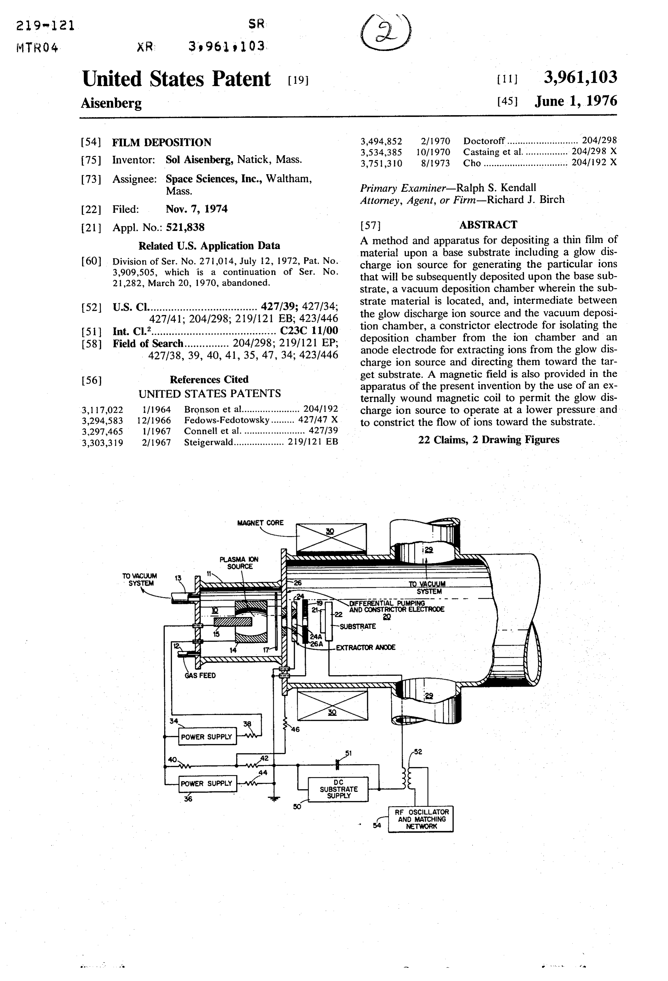
PASMA ON SNNSN rS
Ess
RF OSCILATOR
AND MATCHING
NETWORK
Page 2
Drawing sheet — no readable text.
Page 3
Occurs within this source of ions, and the desired mate
FILM DEPOSITION rial is converted into a plasma form with the ions to be CROSS-REFERENCE TO RELATED APPLICATION deposited in a mixture with high energy electrons. An axial magnetic field may be used to constrain the orbits
This application is a division of application Ser. No. of the electrons and increase their likelihood of ioniz 271,014 filed July 12, 1972, which is now U.S. Pat. No. ing atoms of the material under consideration. This 3,904,505, issued Sept. 9, 1975, which in turn is a magnetic field permits the electrical discharge to oper continuation application of my previously filed applica ate at a lower gas pressure than could be used without tion, Ser. No. 21,282 filed March 20, 1970, abandoned, 10 the magnetic field. Thus, in the source discharge cham for FILM DEPOSITION. ber, there is a plasma which contains a large concentra
BACKGROUND OF THE INVENTION
tion of ions of the species that are to be subsequently deposited.
The present invention relates to a method and appa A plasma discharge from this plasma ion source is ratus for providing improved thin film deposition. generated into a vacuum deposition chamber where the There have been numerous techniques employed for 15 substrate material is located. This can be accomplished depositing thin films, most of which involve the use of by locating an extraction electrode in the vacuum de a substrate, which is elevated to or maintained at a position chamber and by the use of a constrictor means relatively high temperature. This high substrate tem separating the higher pressure plasma ion chamber perature has been considered necessary during the 20 from the lower pressure vacuum deposition chamber. deposition of the thin film for the purpose of increasing The ions are extracted through an aperture in the con the mobility of the atoms being deposited. However, strictor by means of the applied electric field which this high temperature substrate has certain problems maintains a discharge between the plasma source, associated with it. For example, one disadvantage of which functions as a cathode, and the extraction elec vapor deposition upon a hot substrate is that the impu 25 trode, which is situated in the vacuum deposition rities are caused to diffuse out from the substrate and chamber. The purpose of the constrictor means is to thereby affect the composition of the thin film that is isolate the vacuum deposition chamber from the higher being deposited. Further, the excess temperatures pressures present in the plasma ion chamber while the cause a poor definition at the junction between the film extractor electrode pulls the positive ions within the and the base substrate material. plasma source toward the target substrate. It is often It is known that the necessary substrate atom mobil 30 desirable to surround the constrictor aperture with the ity is obtained by heating the incident ions that are to same material as that to be deposited on the substrate. be deposited on the substrate surface rather than the In another embodiment of the invention the acceler substrate itself. The apparatus of the present invention ated beam may be of an inert gas and the ions to be takes this fact into account and permits less heating of deposited may be supplied by an auxiliary source the substrate by isolating the substrate within a sepa 35 within the deposition chamber. The beam provides the rate chamber adjacent to the plasma ion source cham energy necessary to deposit the ions from the source ber. Further, the apparatus is designed to control the which co-impinge with the ion beam. energy of impinging ions by appropriate biasing means coupled to the substrate material. BRIEF DESCRIPTION OF THE DRAWINGS 40 These and other objects and advantages of the pre
It is an object of the present invention, therefore, to provide an improved method and means for the deposi sent invention will be more clearly understood when tion of thin films. considered in conjunction with the accompanying It is another object of the present invention to pro drawings in which:
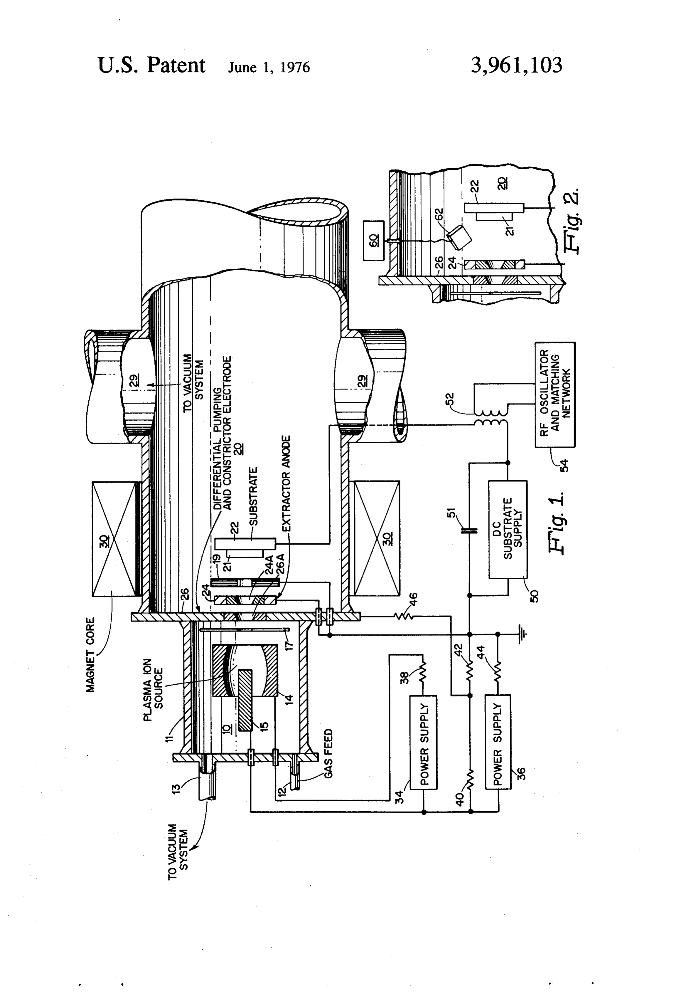
vide film deposition apparatus wherein the substrate 45 FIG. 1 is a cross-sectional diagram of one embodi can be maintained at a relatively low temperature. ment of the deposition system according to the inven A further object of this invention is to provide a tion.
method for fabricating a thin film-substrate structure FIG. 2 is a cross-sectional view of part of another wherein the film can be deposited at a high rate and in embodiment of the deposition system similar to that a controllable manner. shown in FIG. 1.
Another object of the present invention is to provide 50 DETALED DESCRIPTION a thin film upon a base substrate wherein there has been little or no impurity diffusion from the substrate As hereinbefore mentioned, the present invention affecting the thin film deposited thereon. permits the deposition of improved thin films by means Still another object of the present invention is to of an ion beam source used in conjunction with a vac provide a thin film-substrate structure wherein the 55 uum deposition chamber. FIG. 1 shows an embodiment junction between the two substances is well defined. for practicing the present invention. In one particular Other objects of the present invention will become system, a silicon film 21 is deposited on a single crystal apparent upon reading the detailed description in con silicon substrate 22. The film 21 is shown in an exagger junction with the drawings and appended claims. ated thickness in FIG. I.
60 Plasma ion source 10 generally includes chamber
SUMMARY OF THE INVENTION structure 11 having vacuum line 13 and gas input line One embodiment of the apparatus of the present 12 connected thereto. Vacuum line 13 connects to a invention provides a means by which the thin film is vacuum pump (not shown) which controls the pressure formed on a substrate by ionizing and electrostatically 65 in source 10. Also included in ion source 10 are silicon accelerating a beam of atomic particles of a material electrodes 14 and 15, which connect externally to which is to be deposited on the substrate as a thin film. power supply 34 and resistor 38. With an electrical A plasma ion source acts as such a source of atoms of discharge taking place within plasma ion source 10, the thematerial to be deposited. An electrical discharge material which is silicon in this particular case, is intro
Page 4
duced into a plasma formed by the high energy elec 30, and this in turn serves to maintain the plasma con trons. A magnetic field set up by magnetic coil 30 influ striction and permits a large fraction of the extracted ences the formation of the ions within plasma ion positive ions to pass through the anode aperture, subse source 10 by constraining the orbits of the electrons quently impinging on substrate 22. The apertures in the and increasing the likelihood of ionizing atoms of sili electrodes 24 and 26 permit differential pumping to con. This external magnetic field permits the electrical occur, thereby maintaining a good vacuum (about 10 discharge to operate at lower gas pressure than could Torr) in deposition chamber 20 (provided via vacuum be used without the magnetic field. line 29), while somewhat higher pressure is maintained The generation of an ionized plasma usually can in plasma ion source 10. It is often desirable to sur occur through a neutral gas such as argon, hydrogen, or 10 round the apertures in electrodes 24 and 26 with the helium, or through a more active gas, such as nitrogen same material as that to be deposited on the substrate. or oxygen or a mixture thereof, introduced via line 12. Note that the magnetic field serves three purposes: In The ions produced in this source deposition chamber in the plasma ion source it permits the source to operate turn tombard the cathode (electrodes 14 and 15) and at lower pressures; it aids in constricting the plasma sputter or vaporize atoms of material into a discharge 15 through the constrictor electrode; and it helps to main space where they can be ionized. Thus, in the plasma tain the plasma in a constricted path on its way to the ion source 10, there is produced a plasma which con substrate.
tains large concentrations of ions of the species that The constrictor electrode 26 may be left essentially one wishes to deposit upon substrate 22. electrically floating through a high impedance resistor Many times it is desirous to obtain mixtures of ions 20 46 to an appropriate potential such as the one deter such as aluminum and oxygen, silicon and oxygen, or mined by the resistors 40 and 42. For the embodiment silicon and nitrogen, for the deposition of insulating of FIG. 1, this potential is intermediate between the layers, such as aluminum oxide, silicon dioxide, or potential of the cathode in source 10 and the anode in silicon nitride. There are generally two different ap 25 chamber 20. Similarly, the insulating shield 17, posi proaches. One approach is to use electrode material tioned between electrodes 14 and 20, may be left float fabricated of silicon or aluminum and to introduce the ing. Shield 17 minimizes the tendency of the discharge necessary oxygen or nitrogen gas into the plasma by to attach other than where desired. A focusing elec means of the appropriate gas feed line 12 for the main trode 19 can also be used between anode 24 and sub tenance of this ion plasma. There may be difficulty, strate 22. Electrode 19 is shown connected to anode however, with this approach since adjusting the partial 30 24, but can be connected to a separate biasing supply if pressures of the oxygen or nitrogen in order to obtain desired thereby controlling the final path of the ion the correct film stochiometry appears to be difficult. beam.
An alternative way, which appears to be advantageous The potential on substrate 22 relative to that of is to fabricate the electrode material of the necessary 35 plasma ion source 10 and extractor anode 24 deter materials, such as silicon oxide or nitride. One then mines in large part of the kinetic energy with which the introduces the correct mixture into the plasma source positive ions impinge on substrate 22. Reference is by operating a glow discharge between the two elec directed to substrate supply 50 which connects via the trodes in the ion source chamber 10. Consideration of secondary winding of transformer 52 to substrate 22. other types of films is taken up later after a discussion The combination of the DC power supply 50 with the of the operation of the deposition chamber. 40 by-pass capacitor 51 permits a DC bias to be applied to The next occurence in the operation of the apparatus the substrate while maintaining the power supply at a is the extraction of the plasma discharge from the low impedance relative to ground. An AC or RF volt plasma ion source 10 into vacuum deposition chamber age is superimposed on the DC bias voltage by means 20 where the substrate 22 is located. To facilitate this, of oscillator 54 and transformer 52. The use of the an anode extraction electrode 24 is located in deposi 45 transformer permits the application of an additional tion chamber 20 along with a constrictor electrode 26. AC voltage without modifying the DC bias voltage The purpose of constrictor electrode 26 is basically to provided by the DC supply 50.
separate the higher pressure sputtering source chamber As previously mentioned, the axial magnetic field 10 from the lower pressure film deposition chamber 20. helps maintain the ion beam in a columnated mode The ions are extracted through the constrictor elec 50 after it is extracted through the aperture in anode 24 trode 26 by means of the externally applied electric and minimizes space charge spreading. In this way, one field, which maintains a discharge between the plasma can achieve a higher deposition rate than would other source 10, operated as a cathode, and the extractor wise be expected in the absence of a magnetic colum anode 24, located in deposition chamber 20. Anode 55 nating field.
supply 36 facilitates the foregoing by biasing the anode There are some modifications of the deposition sys positively with reference to the source 10. The external tem of the present invention that will enable the deposi electric field generated by power supply 36 is oriented tion of either conducting films on insulating substrates along the external magnetic field caused by magnetic or depositing insulating films on conducting or insulat coil 30 so that the plasma is extracted along magnetic 60 ing substrates. The necessity for these modifications field lines. This serves to maintain the plasma in a con relates to the fact that when depositing an insulating stricted mode so that it is able to pass through the substrate of film it is more difficult to control the en aperture 26A in constrictor electrode 26 more effi ergy of the ions impinging on the substrate 22, and ciently. Anode electrode 24 acts to extract electrons therefore is necessary to prevent the surface from from the plasma source, and the electric field gener 65 building up to a positively charged repelling condition. ated by the extracted electrons pulls the positive ions In the present invention, as shown in FIG. 1, this has from plasma source 10 along with them. The anode 24 been remedied by using an rf power supply 54. has an aperture 24A in it located along the axis deter The AC or rf supply, which connects via transformer mined by the magnetic field produced by magnetic coil 52 to substrate 22, operates at a high frequency (at
Page 5
S 6 about 15Kc or 13 megacycles, for example) and is used The use of this ion deposition technique has shown, to alternately bias the substrate surface positive and for example, that insulating films of carbon can be negative by using the displacement current that flows deposited with material properties very similar to that through the insulating film or substrate. The alternating of carbon in the diamond form. The observed points of positive and negative potential applied to the substrate similarity between the ion beam deposited carbon form is used to extract positive ions and electrons from the and a diamond-like material consists of the following: plasma so that the net current to the surface is zero; but (1) high index of refraction, (2) high electrical resistiv at the same time, during portions of the cycles, positive ity, (3) transparency in the visible range, (4) high di ions can be attracted to the surface. The rf amplitude 10 electric constant, (5) ability to scratch glass. These applied to the substrate determines the energy of the insulating hydrofluoric carbon films also show a high resistance to acid etching. One advantage of insulating positive ions attracted to the surface and can be used to control the deposition energy. carbon films is that such films are quite resistant to FIG. 2 shows a partial view of the system of FIG. 1 sodium ion diffusion through these films which occurs which has been adapted for practising another embodi 5 at elevated temperatures. This is in agreement with ment of the invention. A vaporizing source 62 and like what would be expected for a densely packed diamond associated power source 60 are added to the configura boundaries carbon structure which has densely packed grain tion of FIG. 1. Source 62 is located in chamber 20 near and resists the motion of relatively large to substrate 22. In practising this embodiment of the films can thereforeinsulating alkali ions. Stable and semiconductor carbon be produced by this technique and invention, the introduction of energy into the surface 20 it is expected that the atoms of the vaporizing source is primarily to effect find widespread use intechniques of the invention will the semiconductor field.
vaporization, with the energy to effect deposition on Mixtures of gases or vapors can also be used to de the substrate being primarily supplied by an energetic posit various film compounds. For example, tungsten beam of gaseous ions. This can be accomplished by and carbon mixtures or compounds thereof can be using an argon beam, for example, generated from the 25 deposited in the tungsten carbide form by using either plasma source in conjunction with a source of atoms to tungsten and carbon electrodes or, for more rapid de be deposited and located in chamber 20. Thus, an ener position by introducing a tungsten compound in the getic beam of gaseous ions, such as argon or another gaseous form and a hydrocarbon compound in the inert gas, coimpinge on the substrate surface with gaseous form into the plasma ion source atoms from source 62. Within one or two collisions the 30 Apparatus similar to that shown in FIG. region.1 can be used high kinetic energy of the argon ion beam is transferred to deposit a carbon-diamond film. The electrodes 14 to the lower energy neutral film atoms to be deposited and 15 may be made of carbon, and the mixture gas on the substrate surface and gives them the necessary may be methane for example (a hydro-carbon gas). mobility so that they can nucleate and form an im proved film. For example, with the embodiment of FIG. 35 The carbon ions are introduced into a plasma from ion source 10 by sputtering from the electrodes themselves 2 one could deposit silicon films on a substrate by or from the gas.
means of thermal vaporization of silicon from source By means of the acceleration potential applied to the 62, concurrently with impingement on the surface of a substrate, it is possible to have the ions come in with a high energy argon beam, for example. This beam moderately high kinetic energy (about 100 electron should provide the necessary kinetic energy to transfer 40 volts for example). As a result of this large kinetic to the silicon atoms by means of argon-silicon collisions energy of the incidentions, these ions when they strike on the surface. the deposition surface retain a very high surface mobil Source 62 is shown schematically but can be any one ity and can move about to nucleate into a single crystal of various types of sources of atoms. For example, structure. At the same time, the carbon atoms already source 62 may be a sputtering source, a crucible-type 45 on the deposition surface, in the process of scattering vaporization source or even a resistively heated ribbon. the incident ions themselves, will pick up kinetic en There are other ways that a deposition material can ergy and become mobile. Thus, the incidention and the be introduced into the source plasma. One is by sput first few surface monolayers of the deposition surface tering of material from the electrodes 14 and 15, of are at a relatively high energy compared to that of the FIG. 1. Thus, a silicon electrode would be used for the 50 basic substrate. These surface atoms retain enough deposition of silicon films, while a carbon electrode energy so that they can nucleate into a diamond-like would be used for the deposition of carbon films. me single crystal structure.
tallic electrodes, of course, can be used for the deposi Therefore, the apparatus of the present invention can tion of metallic films. An alternative way of introducing be used to deposit various types of films on different the deposition material into the plasma at a much faster 55 substrates and does so by an ion beam technique, rate is by the introduction of the deposition material in wherein the degree and uniformity of deposition are the vapor or gaseous form or as a component of a gase controlled. The apparatus can also be implemented for ous additive material and the subsequent decomposi use with a vapor source, which is usually located in the tion of the gaseous additive material into the appropri deposition chamber. Such an arrangement has also ate ions by means of the energy of the plasma. This is a 60 been used to supplement the deposition from the ion form of plasma pyrolysis. The use of a hydrocarbon gas, beam. In other words a beam containing silicon ions for example, in chamber 10 can permit the deposition could be used with a silicon vapor source. Another film of carbon films on the substrate since the ions exiting so deposited was molybdenum.
from the ion source will consist of carbon ions and of Another feature of the invention is that relatively hydrogen ions. The hydrogen ions incident on the sub 65 small layers of diamond-like carbon can be deposited. strate will help to remove residual oxygen ions that may Usually for carbon to form into a diamond-like crystal be on the substrate and thus, enhance the subsequen lographic structure it is necessary that the carbon deposition of the carbon ions. . .. . atoms be in a high temperature, high pressure, environ
Page 6
ment for a sufficiently long time so that the crystalliza of said spaced electrodes and said substrate contained tion into a diamond form can occur. The technique within said deposition chamber.
used herein employs an energetic ion beam that does 7. The method of claim 6 wherein said electrical not require high pressures since only a small portion of potential is an AC voltage.
the carbon is heated to a high temperature at one time. 5 8. The method of claim 5 wherein the gas maintained Having described some of the features, objects and within said gas-containing chamber is capable of sup advantages of the invention, other modifications of and plying a portion of the material which is to be deposited departures from the embodiments disclosed herein will after becoming ionized in said gas-containing chamber. become apparent to those skilled in the art all of which 9. The method of claim 8 wherein said material to be are contemplated as falling within the spirit and scope 10 deposited is carbon and wherein at least one gas within of the invention and are to be limited solely by the the gas-containing chamber contains carbon as a con appended claims. stituent thereof.
What is claimed is: 10. The method of claim 9 wherein said gaseous ions 1. A method for depositing a film on a substrate 15 are carbon ions and the film deposited on the substrate comprising the steps of: is a film of carbon having diamond-like characteristics. a. generating an energetic beam of gaseous ions, 1. The method of claim 10 wherein said ions are which may be of the same material as the film to be carbon ions and the film deposited on the substrate is a deposited, by means of a glow discharge ion carbon film having the characteristics of a high index of Source; refraction, high electrical resistivity, transparency in b. producing a pressure differential between said 20 the visual range, a high dielectric constant and the glow discharge ion source and a deposition cham ability to scratch glass.
ber containing therein the substrate on which the 12. A method for depositing a film on a substrate film is to be deposited together with a source of comprising the steps of:
deposition atoms of the same material as the film to 25 a. generating an energetic beam of gaseous ions in a be deposited; and, gas-containing chamber, wherein said chamber c. directing said energetic beam of gaseous ions into contains at least one gas capable of supplying a said deposition chamber such that the beam of ions portion of the material which is to be deposited, by impinges concurrently upon the substrate and said means of establishing a sufficient electrical poten source of deposition atoms and thereby deposits a 30 tial between at least two spaced electrodes so as to film of the deposition material on the substrate. cause a glow discharge therebetween which ionizes 2. The method of claim 1 wherein said energetic said gas capable of supplying a portion of the mate beam of gaseous ions includes ions of an inert gas. rial which is to be deposited to form ions thereof; 3. The method of claim 2 wherein said inert gas in b. producing a pressure differential between said
gas-containing chamber and a deposition chamber 4. The method of claim 1 wherein said source of containing therein the substrate on which the film deposition atoms includes silicon atoms. is to be deposited;
5. A method for depositing a film on a substrate c. extracting said gaseous ions from said gas-contain comprising the steps of: ing chamber by means of an extraction electrode a. generating an energetic beam of gaseous ions in a 40 said having an aperture disposed therein and containing gas-containing chamber by means of establishing a ions by means of an axial magnetic field be sufficient electrical potential between at least two tween said gas-containing chamber and said depo spaced electrodes, of which at least one of said sition chamber with the axis of the magnetic field electrodes is at least partly formed of the material being substantially parallel to the axis of said ex which is to be deposited, so as to cause a glow 45 d. traction electrode aperture; and, accelerating at least some of said gaseous ions and discharge therebetween which releases atoms of directing them into said deposition chamber so as the material which is to be deposited from said to impinge upon said substrate thereby depositing a electrode at least partly formed of said material film on the substrate.
and ionizes said released deposition material atoms 13. The method of claim 12 further comprising the to form ions thereof; 50 step of applying an electrical potential between at least b. producing a pressure differential between said one of said spaced electrodes and said substrate con gas-containing chamber and a deposition chamber tained within said deposition chamber.
containing therein the substrate on which the film 14. The method of claim 13 wherein said electrical is to be deposited; potential is an AC voltage.
. extracting said gaseous ions from said gas-contain 55 15. The method of claim 12 wherein said material to ing chamber by means of an extraction electrode be deposited is carbon and wherein at least one gas having an aperture disposed therein and containing within said gas-containing chamber contains carbon as said ions by means of an axial magnetic field be a constituent thereof. - tween said gas-containing chamber and said depo 16. The method of claim 15 wherein said material sition chamber with the axis of the magnetic field 60 which is to be deposited is carbon and at least one of being substantially parallel to the axis of said ex said spaced electrodes is formed of carbon. traction electrode aperture; and, 17. The method of claim 15 wherein said gaseous d. accelerating at least some of said gaseous ions and ions are carbon ions and the film deposited on the directing them into said deposition chamber so as substrate is a film of carbon having diamond-like prop to impinge upon said substrate thereby depositing a 65 erties.
film on the substrate. 18. The method of claim 17 wherein said ions are 6. The method of claim 5 further comprising the step carbon ions and the film deposited on the substrate is a of applying an electrical potential between at least one carbon film having the characteristics of a high index of
Page 7
refraction, high electrical resistivity, transparency in 21. The method of claim 19 further characterized by the visual range, a high dielectric constant and the the use of an electrically insulating shield means posi ability to scratch glass. tioned between said spaced electrodes and said con 19. The method of claim 12 wherein said pressure 5 strictor electrode means, said shield means having an differential between the gas-containing chamber and aperture disposed therein through which said ions flow. the deposition chamber is produced by constrictor 22. The method of claim 21 wherein said shield electrode means having an aperture disposed therein means aperture, and constrictor electrode means aper through which said beam of gaseous ions can pass. ture, and said extraction electrode aperture are lined 20. The method of claim 19 wherein said constrictor electrode means aperture and said extraction electrode 10 with
a material which is the same as the material which be deposited. sk ck ck ck sk aperture are lined with a material which is the same as the material which is to be deposited.
Provenance
- Collection
- Cited prior art
- Original PDF
- patentimages.storage.googleapis.com →
- Filed
- 1974-11-07
- Pages
- 7
- Method
- pdftotext (the PDF's own text layer) + pdftoppm 300dpi page scans
- Source
- Google Patents bibliographic record
- Granted
- 1976-06-01
- Inventors
- Sol Aisenberg; Space Sciences Inc
- Transcribed from
- patentimages.storage.googleapis.com →