patent · US5504514
System and method for solid state illumination for spatial light modulators
2 April 1996
Page 1 — bibliographic record
United States Patent (19) 11 Patent Number: 5,504,514 Nelson 45 Date of Patent: *Apr. 2, 1996 (54) SYSTEMAND METHOD FOR SOLID STATE 4,907,034 3/1990 Doi et al. ................................ 355/327 LLUMINATION FOR SPATAL LIGHT 4,927,230 5/1990 Tokumitsu ... 350/96.24 MODULATORS 4,935,665 6/1990 Murata ..... ... 362,800 X 5,032,960 7/1991 Katoh ... ... 362,244 X 75) Inventor: William E. Nelson, Dallas, Tex. 5,041,851 8/1991 Nelson .................................... 346,160 5,043,716 8/1991 Latz et al................................ 340/782 5,055,855 10/1991 Nishio .......... ... 34.6/107 RX (73) Assignee: Texas Instruments Incorporated, 5,138,340 8/1992 Sprague et al. ......................... 34.6/108 Dallas, Tex. 5,144,117 9/1992 Hasegawa et al. ... ... 362,800 X 5,151,718 9/1992 Nelson ................................ 355/229 X * Notice: The term of this patent shall not extend beyond the expiration date of Pat. No. FOREIGN PATENT DOCUMENTS 5,151,718. 0332953 9/1989 European Pat. Off..
21 Appl. No.: 359,358 62-127707 10/1987 Japan.
22 Filed: Dec. 19, 1994 2-386 1/1990 Japan.
Related U.S. Application Data
Primary Examiner-Nestor R. Ramirez 63) Continuation of Ser. No. 170,435, Dec. 20, 1993, aban Attorney, Agent, or Firm-Julie L. Reed; James C. Kester doned, which is a continuation of Ser. No. 835,80, Feb. 13, son; Richard L. Donaldson 1992, abandoned,
(52 U.S. C. ... 347/130; 347/134; 362/800 There is disclosed an optic system for illuminating a spatial 58 Field of Search ..................................... 347/130, 134, light modulator array in a Xerographic printing process 347/135; 355/228, 229; 250/494.1; 362/235, consisting of an array of LED emitters constructed to 244, 249, 800 efficiently replace the conventional tungsten source used in prior art. The array of LED emitters can be geometrically 56 References Cited configured or electrically operated by strobing or varying the brightness of individual pixels to compensate for other
4,428,647 1/1984 Sprague et al. .................. 250/494.1 X process. By exposure strobing the LED source correction for 4,700,206 10/1987 Yamakawa .............................. 346/60 fuzzy line edges can be achieved.
4,734,734 3/1988 Yano ....................................... 355/218 4,856,863 8/1989 Sampsell et al. .................... 350/96.6 4 Claims, 4 Drawing Sheets
Page 2
Drawing sheet — no readable text.
Page 3
Drawing sheet — no readable text.
Page 4
Drawing sheet — no readable text.
Page 5
Drawing sheet — no readable text.
Page 6
SYSTEMAND METHOD FOR SOLD STATE all of the light collected by the condenser lenses can be LLUMINATION FOR SPATAL LIGHT concentrated on the spatial light modulator active area. MODULATORS The latter problem exists for printing systems in that a spatial light modulator array is necessarily elongated or
This application is a Continuation of application Ser. No. 5 linear in aspect, and thus the light pattern reaching the array 08/170,435 filed Dec. 20, 1993, which is now abandoned, must be wider than it is high by a significant proportion, which is a continuation of application Ser. No. 07/835,180 compared to either the filament aspect ratio or the aperture filed Feb. 13, 1992, which is now abandoned. of the imager. Because the image of the source must simultaneously come to focus on the imaging lens circular
O aperture and at the same time uniformly illuminate the full
TECHNICAL FIELD OF THE INVENTION
length of the spatial light modulator which is maintained
This invention relates to a spatial light modulators and between the aperture of the collimator lens and the imaging more particularly to illumination systems and methods of lens, and since the spatial light modulator is substantially operation for such devices. wider than it is high, in order to fully illuminate the array the 15 resulting aspect of the light necessitates considerable width
BACKGROUND OF THE INVENTION of illumination above and below the active area of the spatial light modulator device that is subsequently "wasted'.
Semiconductor light modulators, such as deformable mir Another problem is that the focused image from the ror devices (DMD), liquid crystal arrays, and electro-optic 20 spatial light modulator is continuously projected onto a crystals, are gaining in popularity as a replacement for the moving drum. Thus, during the exposure period of a dot laser polygon Scanner in Xerographic printing processes. A line, for any pixel image location the drum will rotate a technology of preference, due to its monolithic, semicon given distance and broaden or blur that pixel image. A plot ductor fabrication process, is the deformable mirror device of the light energy on the drum for that pixel location will (DMD). Issued U.S. Pat. No. 5,061,049 entitled "Spatial 25 reveal that the maximum light energy transferred to that Light Modulator Printer and Method of Operation', pixel will reach a peak level only at the centroid of the pixel assigned to the common assignee with this patent applica and will build up to that point and fall off from that point in tion, which patent is hereby incorporated by reference the shape of a pyramid. This pyramidal spreading of the herein, discusses one embodiment of a spatial light modu pixel energy is not optimum for minimum feature formation lator using a tungsten light focused via optics on a spatial 30 and thus reduces the sharpness of the xerographic image in light modulator array. While the invention in that application the process direction.
functions very well, several areas of improvement have A further problem with existing spatial light modulator become apparent. structures and systems is the fall-off of the light energy on These improvements center around the reduction in power the outer periphery of the spatial light modulator array, consumed, reduction in overall physical size of the system 35 particularly with elongated arrays, due to the difficulty in and improved uniformity of illumination across the spatial collecting and directing light energy from lambertian fila light modulator array. Tungsten sources, like all incandes Ilent SOurces.
cent filaments, emit light, more or less isotropically, which A still further problem with such existing systems is that must be collected and focused by condensing optics if the optic intensity is not constant or uniform over the whole light energy is to be efficiently utilized by the modulator 40 filament array and there is not a practical method for elements. In addition, a major byproduct of incandescent adjusting the optic characteristics of the light source after light is the production of heat which in turn demands an manufacture.
ability of dissipating the heat. This, in turn, requires bulky Another problem is that the generally available tungsten structures, or plenums, to move the heat away from the source, as well as fans with their inherent noise/reliability 45 mum sources light for have filament aspect ratios that are not opti spatial light modulator light modulator systems.
Another problem is the relatively limited lifetime of the
Because incandescent light is lambertian in its emission tungsten sources.
character, the rays must be collected from all sides of the A final deficiency of the tungsten source is that of the filament and focused, thereby requiting fast optics which again argues for large size and cost, to avoid wasted power 50 impossibleinertia, thermal
or lag time of the filament, making it vary the light output of the source within a due to collection inefficiencies.
printing line time, as is desirable to compensate for specific
Accordingly, one problem in prior art spatial light modu printing deficiencies.
lator structures is the excessive power required to support the light source coupled with large size, both for the optics SUMMARY OF THE INVENTION and for heat disposition. The aforementioned patent appli 55 cation shows the spatial light modulator array positioned in A solid state optical source, such as a light emitting diode the light energy stream between the light source and the (LED) array, has been substituted for the tungsten light imaging lens aperture. In order to achieve maximum energy source in conventional spatial light modulator systems. The transfer, it is necessary to fill the imager aperture with the LED array can, in one embodiment, be fashioned as a single modulated light image from the spatial light modulator 60 unit with individual lenses and LED chips arranged to make array. The imager lens is designed, for cost and other up various array structure configurations. Alternatively the reasons, to be round and thus a nearly square filament image structure can be a substrate of flexible material on which has aspect ratio magnified to overfill the imager, must be pre been fashioned an array of LED chips and lenses. Each lens sented to the lens to insure that the lens is fied. This is associated with an LED emitter or a group of LED arrangement, while performing properly, suffers from the 65 emitters so that the light from said emitters is efficiently problem that not all of the power modulated by the spatial directed and focused onto a particular region of an opposing light modulator can be passed by the imaging lens, and not spatial light modulator array or an intervening optical ele
Page 7
ment that further shapes the ray to bundle prior to the spatial FIG. 9a shows an ideal exposure of a pixel; light modulator. Examples of such modulators include FIG.9b shows the actual exposure in the prior art printing deformable mirror devices (DMD), liquid crystal arrays, and process;
electro-optic crystals. FIG. 9c shows the exposure strobing that can be accom Additionally, the emitter array could simply be an appro plished with the proposed invention; priate area array comprising numerous individual LED FIGS. 10a, 10b and 10c show the light emission patterns emitters or laser diode elements. This area array could be of LED devices with and without primary collection optics; sawn directly from a production wafer and interconnected to and operate in parallel.
Using this structure and method results in lower total 10 formly FIG. 11 shows a schematic of the present system uni power at the light source and its associated power supply, illuminating the entrance aperture of a secondary requires smaller optics due to the efficient light collection of condenser lens element and then forming a region of uni the integrated lens arrays, and eliminates the need for form illumination and a source image beyond the lens. cooling fans. An added benefit is an ability to adjust the light pattern by the geometry of the array or by flexing the 15 DETAILED DESCRIPTION OF THE substrate structure so as to improve upon any inherent INVENTION nonuniformity of the conventional tungsten source and condenser optics. This enhancement can be accomplished Turning now to FIG. 1a, there is shown light element 10 during the manufacturing process and can also be fine tuned 20 with 50 percent of its light going away from the desired during operation of the systems. direction, and the remainder of the light going off to the right The individual elements of the solid state light source can forming angles theta with respect to a line b normal to the also be electronically adjusted, both at manufacture and plane of element 10. The significance of arrows a, b and c during operation so as to improve the light transfer charac are that this source is a lambertian source for which the light teristics of the spatial light modulator array. intensity looks the same to an observer along any direction, 25 So if one does not collect light rays along arrows a and c,
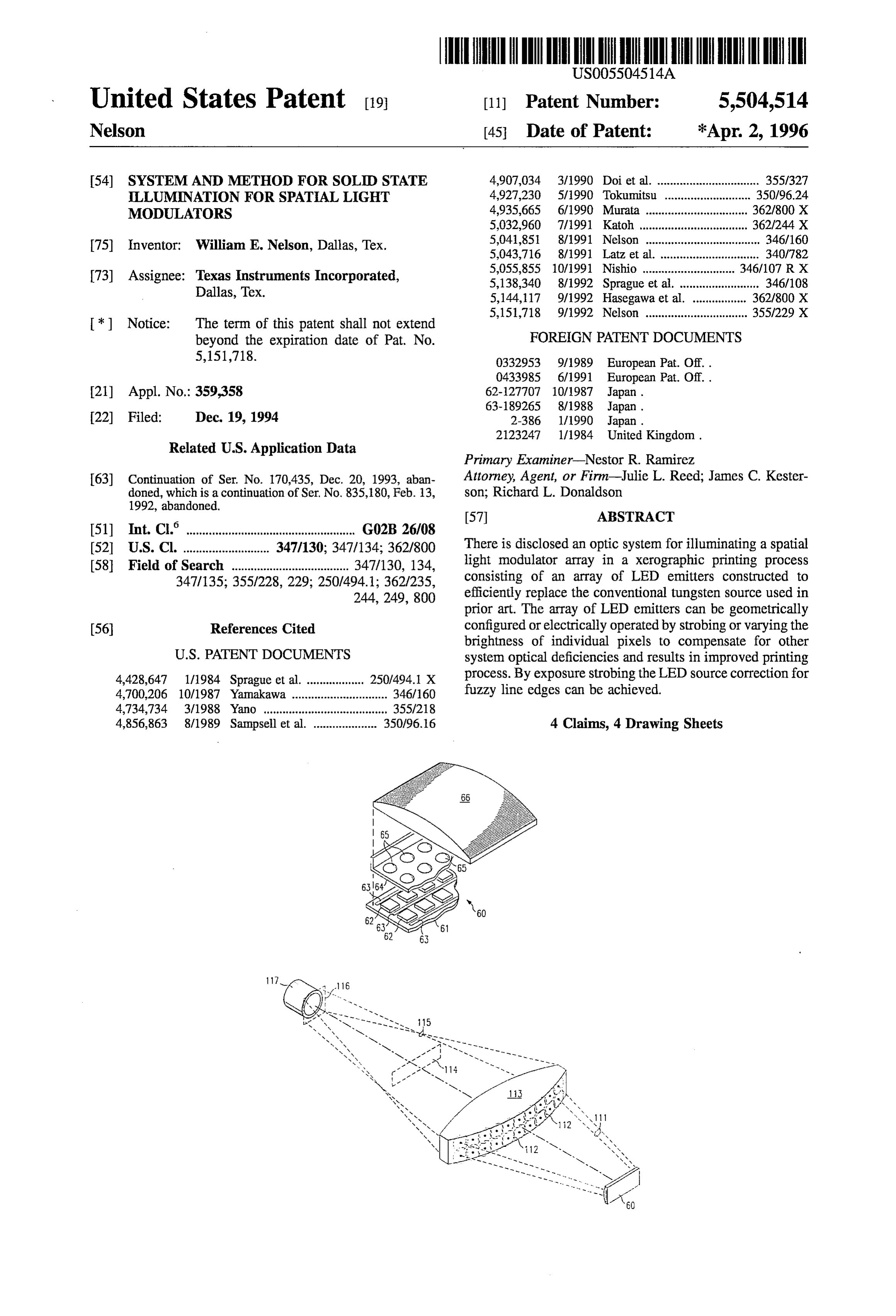
Accordingly, it is one technical advantage of this inven which lie well away from central arrow b, considerable tion that a solid state light source, such as an LED array, or portions of the available light energy will be lost. That is in a surface emitting laser diode array, can be used as a addition to the loss out of the back side of the filament. The replacement for the incandescent light source in a spatial filament 10 is indicated as having dimensions x by y which light modulator array. 30 typically are not the desired format for the light source for It is a further technical advantage of this invention that a a spatial light modulator system. Examples of such modu spatial light modulator array is integrated with a compact, lators include deformable mirror devices (DMD), liquid flexible solid state light source that can be adapted or crystal arrays, and electro-optic crystals. configured to allow for optical adjustment to compensate for FIG. 1b shows the effect of a light source 10' when uneven illumination of the spatial light modulator array, as 35 magnified to fill an imager aperture 12. By failing to fill it well as to improve illumination characteristics and modu completely in the vertical direction and overfilling it in the lation efficiency of the spatial light modulator system. horizontal direction it generally results in system inefficien It is a further technical advantage of this invention that the cies as shown by image 10'.
LED illuminator and spatial light modulator light modulator FIG. 1c shows filament 11 radiating into a solid angle and system can together be operated in a manner to improve the 40 illuminating area 11", representing a first lens surface, which print quality of a Xerographic printing process. is a relatively small portion of the total forward area that is BRIEF DESCRIPTION OF THE DRAWINGS of consideration in the collection. This illustrates that any collection optics that do not virtually surround the front side
A more complete understanding of the present invention of the filament are less than 100 percent efficient in collect may be acquired by referring to the detailed description and 45 ing the light. To do so, the lens must be either large, or very claims when considered in connection with the accompa dose to the filament, and less than optimum trade-offs are nying drawings in which like reference numbers indicate forced on the designer. This is a characteristic problem of the like features wherein: incandescent filaments which are lambertjan radiators. FIGS. 1a, 1b and 1c show characteristics of the prior art 50 FIG. 2 shows a prior art system source 20 radiating to filament source light; collection lens 21 separated from the filament by some FIG. 2 shows the prior art source light projected through distance r. The solid angle that collection lens 21 therefore lenses to form an image; represents referring back to FIG. 1c is determined by its FIG. 3 shows a graph of the intensity of prior art light diameter and by that distance r. It simply cannot fill very from a tungsten source indicating the relative wave length 55 much of the forward angle into which the filament in source region of interest for the printing process; 20 is radiating. That light is collected is subsequently redirected onto condenser lens 22 which is a slabbed section
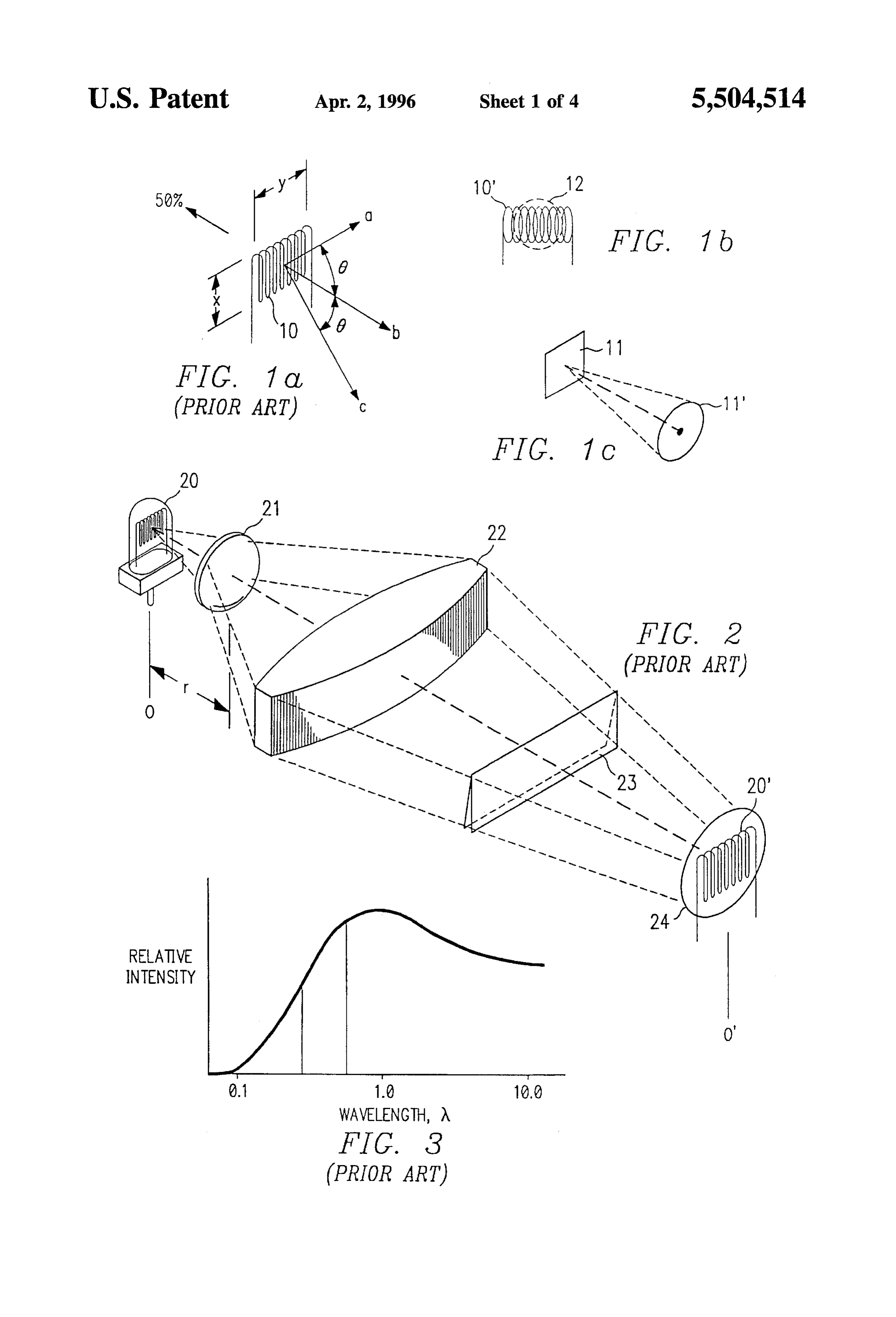
FIG. 4 is a schematic of the elements of the prior process; of an asphere and does not collect the entire bundle of energy FIGS. 5a, 5b and 5c show the problem of illumination that is redirected by lens 21 resulting in a further reduction uniformity with the prior art and the correction or compen 60 in the delivered light converging to area 23, the region of sation with the present art; uniformity where the spatial light modulator device sche FIG. 6 shows a schematic assembly of the LED array and matically resides. This energy is all redirected into filament the initial optics that would go with that module, image 20' at imager lens aperture 24. FIGS. 7a, 7b, and 7c show configurations of LED's on FIG.3 shows a further deficiency of the prior art, namely, Substrates that could be used; 65 that the spectral intensity of the tungsten source at a nominal FIG. 8 shows an LED array substrate with individually temperature of 3,000 K is peaked around 1 micron and the addressable elements; great bulk of the energy radiated lies in the 1-10 micron
Page 8
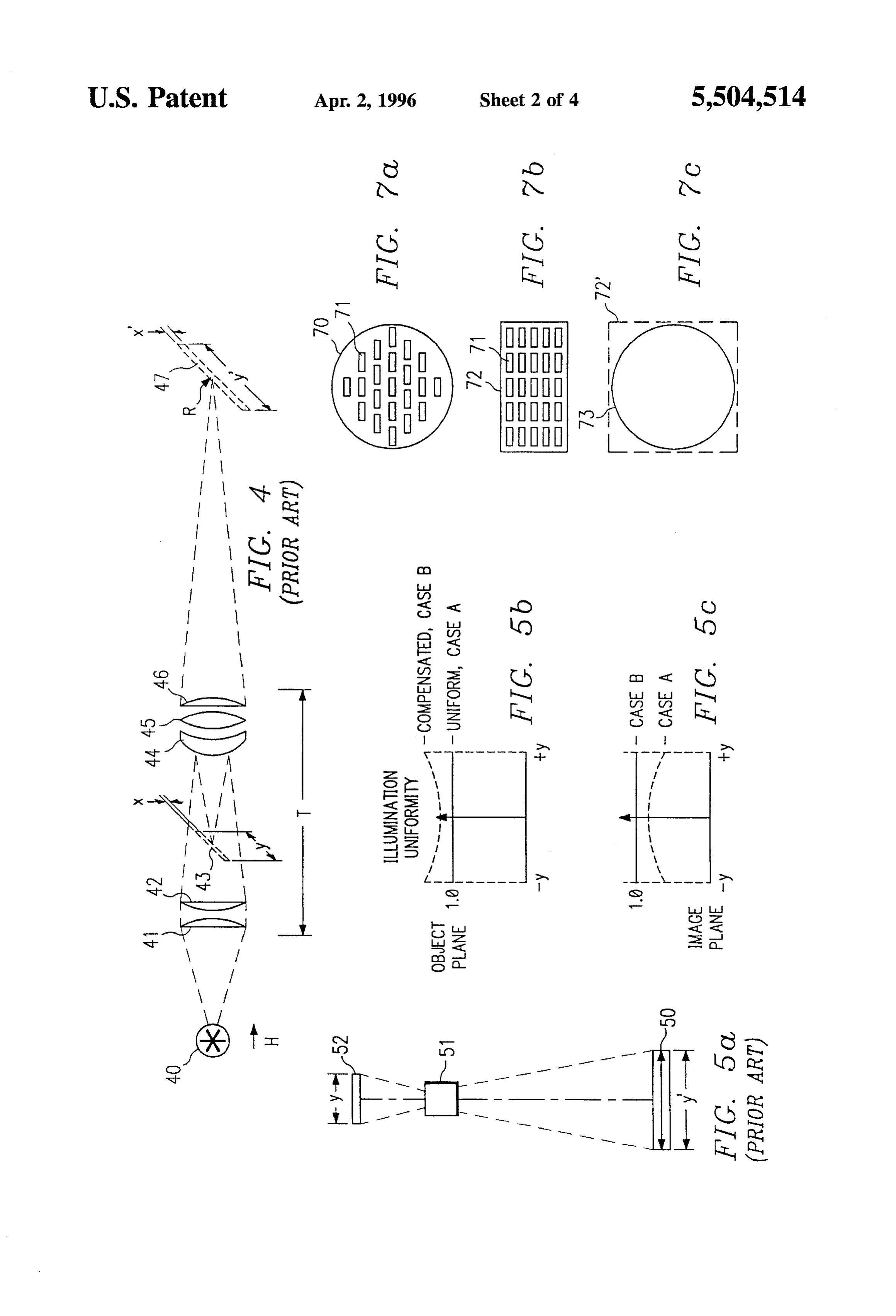
range, that is, as radiated as heat, and very little of it is in the have the lens element 65 still formed above each emitter useful visible range indicated by the band between the lines element 62. Finally, a secondary anamorphic lens 66 may be and which can be utilized in a printing system. positioned above this, and serve to condense the light more FIG. 4 details the radiometry of the prior art as previously efficiently in a preferred direction. The compact assembly discussed in FIG. 2. It shows that any source 40 with radiant thus formed is basically the replacement for the incandes output H falling onto collection lens assembly 41 and 42, cent source in the prior art. A graded index lens array (not thereby illuminating spatial light modulator plane 43, and shown) could also be utilized to collect and direct the LED subsequently reimaging onto imager lens set 44, 45 and 46 illumination.
is subject to a certain efficiency at the image plane 47 solely FIG. 7a shows another possible substrate configuration determined by the brightness of the source H, the transmit 10 70, a circle of diameter Ro which can be precisely the tance of the entire optical system indicated by T, and shown diameter of the imager aperture or smaller, and therefore, as spread across the entirety of the optical components, and can be magnified to precisely fill the circular imager aper the solid angle, that is, the speed of the imager lens assembly ture. It is populated with LED chips 71 to achieve the desired shown schematically by the dottedlines at the output portion radiance levels necessary for the printing process. Another of the imager lens assembly. The final spatial light modu 5 alternative in FIG. 7b shows substrate 72 which is rectan lator image at 47, therefore, has irradiance R, which is gular in nature. It is populated again with LED chips 71. determined by the light collection efficiency, the system This would be magnified anamorphically to fill an imager transmittance and the speed of the imager lens. The only way aperture shown as 73 in FIG. 7c. The most compact and least to improve the irradiance at the image of the spatial light expensive embodiment of rectangular array72 would simply modulator is to either make the source brighter, the imager be a portion of the LED wafer or surface emitting laser diode lens faster, or the system transmittance higher. The system 20 array cut from a production wafer. The desired portion could transmittance is typically improved by optical coatings. That be cut to the desired shape and incorporate a number of is a standard practice in the industry. The speed of the imager individual elements selected to provide the necessary lumi lens and its corresponding aperture can only be increased to nous output.
a practical limit due to the spatial light modulator deflection 25 The dotted line 72 represents the anamorphically mag angle, and because higher speed lenses are larger, more nified substrate from FIG.7b shown as just filling the imager costly, begin to affect the spatial light modulator exposure lens assembly. The benefit of this type of illumination is that module packaging, and generally reach some practical limit each emitter on the substrate shown in FIGS. 7a and 7b is at about a speed of F4.5 due to combined factors. The only equally bright or comparably bright, unlike the case of the remaining variable is to increase the system brightness H at filament source shown in the prior art FIG. 1a and 1b, which the source, or to concentrate the source output power in the 30 has a very non-uniform characteristic. spectral region of interest to the printing process. Typically the filament center is hotter and thus brighter, FIG. 5a showing radiometry in the prior art details an and the edges, particularly where the leads come into the object plane with a small object simulating spatial light filament, are cool and emit far less energy, so when the modulator 52, an imager 51 and an image of the spatial light 35 imager lens is filled, as shown in FIG. 1b, with this filament modulator 50 shown magnified. image, parts of it are much less efficient in the printing FIG. 5b shows the presumed illumination of object 52, process than is the center so maximum advantage of the full where in the uniform perfect case, from the -y to +y position solid angle of the imager lens is not achieved. Referring on the object, it represents a normalized illumination of 1.0 back to FIG. 4, the solid angle of the imager lens is one of across the entire surface and correspondingly when that 40 the key variables in delivering energy to the photoreceptor image is related to the image plane 50, FIG. 5c shows again surface. If one does not effectively fill that imager lens in case A, that the reimaged radiation from the uniform aperture one does not, effectively transmit energy to the spatial light modulator illumination has actually sagged at photoreceptor. The example configurations shown in FIGS. the sides of image as shown at -y' and +y' and is less than 7a and 7b allow one to simulate a radiating source, or a uniform. In the case of the proposed LED illumination 45 physical object that behaves like a filament in the prior art, system, it is possible to increase the brightness at the but which is equally bright at all points, and can be built to extremes of object 52, as shown by the dotted line compen the exact aspect ratio that best serves overall system per sating case B in FIG. 5b, so that more light is delivered at formance. In addition, if the individual LED chips are not the edges of the device than at the center. As a result, when equally bright, or if one fails, the system operation is not too the imager has reformed image 50 with the same tendency 50 compromised. Since each spatial light modulator pixel to roll-off at the ends, we have case B in FIG. 5c, which is images the entire source to the imager, details of the LED schematically represented by a dotted line showing fairly source uniformity are not an extremely critical factor, only constant uniformity of illumination across the entire image the average brightness is of primary significance. from -y' to +y'. FIG. 8 shows an additional embodiment of an LED array FIG. 6 shows the proposed LED illuminator assembly 60 55 on substrate 80 looking very similar to FIG. 7b with the consisting of a primary substrate 61 containing metal con exception that the individual LED chips 71 can now be ductor lines 63 and multiple LED chips shown 62 arranged driven independently through drivers 82 on driver chip 81. in a suitable array positioned with respect to a primary Substrate 80 is possibly separate from driver chip 81, but aspheric multilens array 64 containing lens elements 65 driver chip 81 could be an integral part of substrate 80. The which reside above and capture the radiation from each of 60 point here is that under computer control the programmable the LED chips 62. This is a separate lens array which is dose driver chip can enhance or reduce the light output of the to but does not actually contact the LED devices. As a result, individual elements. The vertical arrow of FIG. 8 indicates each element subtends a large solid angle and is therefore the direction of increasing intensity, indicated by the sche able to receive most of the LED light emission. It is possible matic histograms 83, revealing that the center two elements to form an immersion lens system where the plastic lens is 65 are emitting at a lower light level than the nearest neighbors actually molded over the chips and contains them and seals which are emitting at a lower level than the most outboard them from contamination and environmental problems and elements of substrate 80. For clarity, the LED elements 71
Page 9
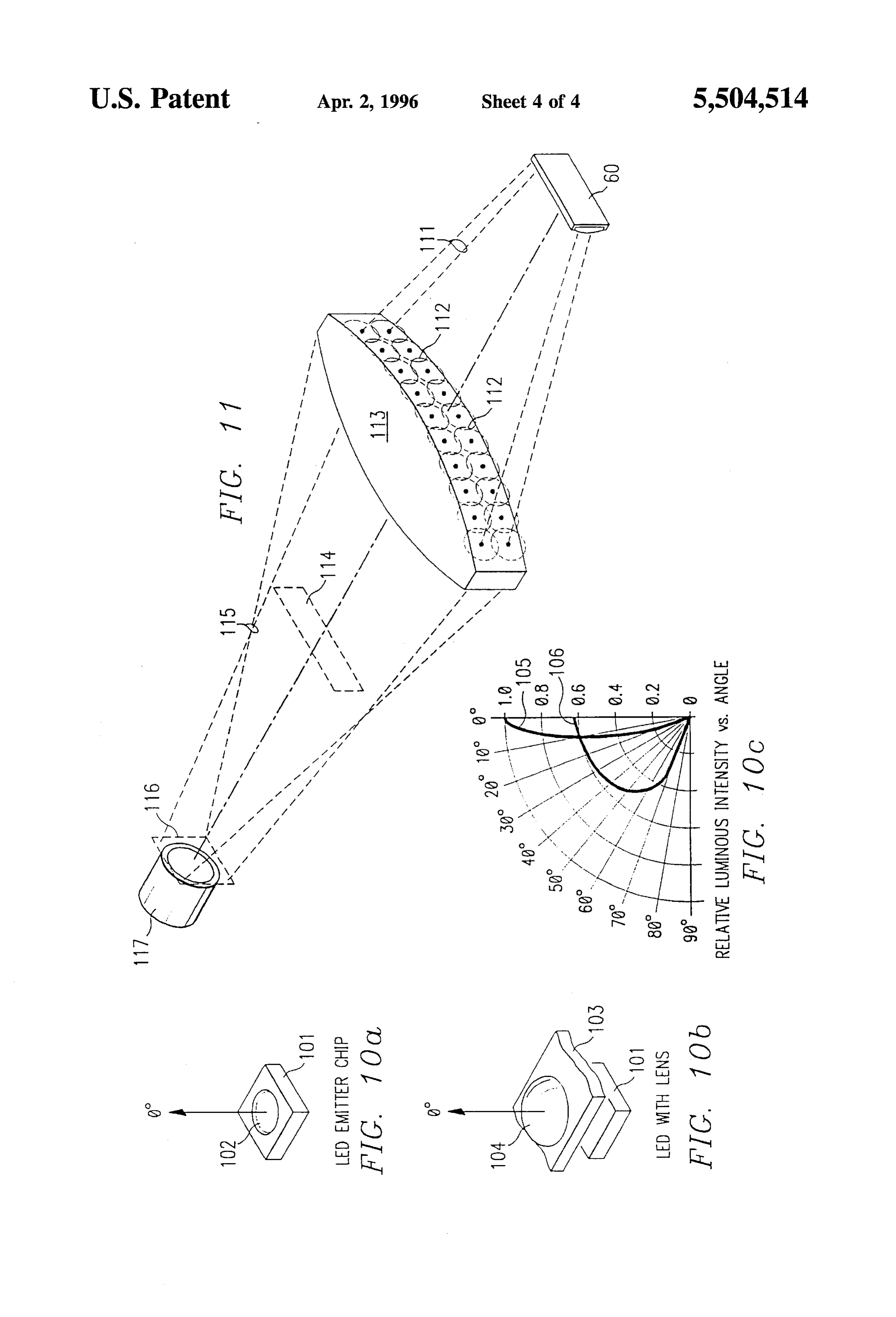
to the left have the histogram omitted. This relates back to FIG. 11 shows a preferred embodiment of the invention FIGS. 5b and 5c where it is proposed to modify the with integrated LED light array 60 having integral lenses. brightness of the illumination from the source to guarantee Ray pattern 111 emanates from LED source 60 and falls on that the image plane radiation levels are uniform and con the input aperture of condenser lens 113. The detail shown stant. So by being able to control the brightness profile of the 5 by circles 112 indicates that the rear aperture of lens 113 is array of LED chips, correction can be made for other uniformly filled by an overlapping array of multiple bundles deficiencies in the optical system and to achieve a uniformly of light emanating from individual LED emitters in array 60 bright spatial light modulator image. Finally, if substrate 70, according to the prescription of FIG. 10b. 72, or 80 were a flexible film, the actual curvature of the Once passing through condenser lens 113, the pattern of array could be tailored to an optical surface or curve, more 10 light proceeds along ray paths 115 to form a magnified compatible with efficient illumination of a condenser ele image 116 of array 60 which completely fills and slightly ment as represented by surface 112 of FIG. 11. overfills the input aperture of imager lens 117. Between FIG. 9a shows an additional advantage of being able to condenser lens 113 and imager 117 lies the region 114 of illuminate the spatial light modulator with an LED array uniform illumination where the spatial light modulator chip source. Because the LED arrays can be turned on and off in 15 will reside in the exposure module system. extremely short periods of time, that is, tenths of microsec Implicit in FIG. 11 is the fact that while the emitter array onds, an option that was not available for a typical incan 60 is a source of nearly monochromatic light, emitted at the descent source, we are able to simulate the ideal exposure in characteristic wavelength of whatever LED material is uti the printing process. FIG. 9a shows an ideal exposure, lized, and falling entirely in the useful band shown in FIG.
indicated as intensity in the vertical direction, appearing as 20 pure the radiation is not coherent as would be the case with a an instantaneous exposure of light energy from a spatial light laser source of illumination. The multiplicity of emit modulator pixel onto the photoreceptor and representing ters are not in phase, hence the disadvantage of coherent sources illuminating very regular periodic structures like the width l which is the desired pixel line width, or the ideal line spatial light modulator array, which results in significant width. energy loss into complex diffraction patterns, is not experi FIG.9b shows what the actual exposure looks like due to 25 enced here, thereby preserving the desired optical perfor the motion of the photoreceptor with a conventional spatial mance features of the conventional incoherent tungsten light modulator under continuous illumination. Because the source. The imager lens 117 can be less complex for the spatial light modulator and the light source remain on for a monochromatic LED array than for the broadband tungsten line time, it actually exposes an area prior to the line of source as well.
interest and after the line of interest and the net result is an 30 Although this description describes the invention with exposed image that is a width w, where w is larger than 1, reference to the above specified embodiments, it is but one which has characteristic light fuzzy edges as shown in FIG. example, and the claims, not this description, limit the scope 9b. This is an undesirable characteristic of the printing of the invention. Various modifications of the disclosed process. A simple way to correct that with the LED source embodiment, as well as alternative embodiments of the of illumination is shown in FIG. 9c, where by exposure 35 invention, will become apparent to persons skilled in the art strobing, that is, turning the LED on for a short period of upon reference to the above description. Therefore, the time at a higher than normal intensity (which is a common appended claims will cover such modifications that fall operating mode for LED chips) the energy can be concen within the true scope of the invention. trated in the region of interest, that is, the line of width l. What is claimed is:
For example, by pulsing the spatial light modulator at 40 1. An improved method of illuminating area array reflec three times the normal intensity, but only for 33 percent of tive spatial light modulators using an optical system com prising:
the line time, the effective exposed line width, while it is slightly wider than the desired line width of l, as indicated generating source illumination from an array of solid-state by width m, is very dose to the ideal case shown in FIG. 9a. 45 light-emitting elements fabricated on a substrate, There is still a little bit of fuzziness to the edges, but by wherein said elements are configured to direct ray shortening the period of exposure the gross blurring of the patterns of individual emitting elements into a bundle edges that is a characteristic of the prior art shown in FIG. of light;
9b is eliminated. positioning a condenser lens having a rear aperture such FIG. 10a shows an individual LED chip 101 and the 50 that said bundles of light from said array of emitting active emitting region 102 referenced to an arrow in the elements uniformly fill said rear aperture of said con forward direction along 0°. FIG. 10b shows a similar chip denser lens and travels through said condenser lens 101 with lens array 103 and individual lens element 104 in along a first optical path; place, again referenced to the arrow along 0°. FIG. 10c providing an imager lens having an aperture along a shows the relative luminous intensity of the LED emitter 55 second optical path, wherein the area between said first versus the forward angle for each of these two chip con optical path and said second optical path comprises a figurations. region of uniform illumination; FIG. 10c shows the relative luminous intensity versus the locating said area array reflective spatial light modulator forward angle on the polar diagram. This shows the forward in said region such that said modulator receives said pattern 105 for FIG. 10b with the lens in place indicating that 60 uniform illumination along a first optical path and it is concentrated along the axis 0 degrees at a relative selected ones of individual elements on said modulator intensity of 1.0. reflect light along said second optical path, wherein FIG. 10c, line 106 is a curve showing the hypothetical said light reflected along said second optical path emission pattern from LED emitter chip 101, FIG. 10a completely fills said aperture of said imager lens; and without a lens showing that there is much more off axis 65 tailoring illumination received by said modulator such energy which is not collected and concentrated in the that said modulator receives a maximum amount of forward direction. said illumination.
Page 10
2. The method as claimed in claim 1 wherein said imager 4. The method as claimed in claim 1 wherein said tailoring lens accepts a maximum amount of illumination energy step further matches the path of the light rays reflected from from said modulator. said modulator to said aperture of said imager lens using said 3. The method as claimed in claim 1 wherein said tailoring solid-state light-emitting elements on said substrate. step further comprises compensating for deficiencies in said 5 optical system. ck k 3 k
Provenance
- Collection
- Cited prior art
- Original PDF
- patentimages.storage.googleapis.com →
- Filed
- 1994-12-19
- Pages
- 10
- Method
- pdftotext (the PDF's own text layer) + pdftoppm 300dpi page scans
- Source
- Google Patents bibliographic record
- Granted
- 1996-04-02
- Inventors
- William E. Nelson; Texas Instruments Inc
- Transcribed from
- patentimages.storage.googleapis.com →